Schottky Diode Applications in Fast Recovery Rectifiers
MAR 24, 20269 MIN READ
Generate Your Research Report Instantly with AI Agent
PatSnap Eureka helps you evaluate technical feasibility & market potential.
Schottky Diode Technology Background and Fast Recovery Goals
Schottky diodes represent a fundamental advancement in semiconductor technology, distinguished by their unique metal-semiconductor junction structure that eliminates the traditional p-n junction found in conventional diodes. This distinctive architecture, first theorized by Walter Schottky in the early 20th century, creates a barrier formed by the contact between a metal and a semiconductor material, typically silicon or gallium arsenide. The absence of minority carrier storage effects inherently enables these devices to achieve switching speeds significantly faster than their p-n junction counterparts.
The evolution of Schottky diode technology has been driven by the semiconductor industry's relentless pursuit of higher efficiency and faster switching capabilities in power electronics applications. Early developments in the 1960s focused on basic metal-silicon contacts, but subsequent decades witnessed substantial improvements in barrier height control, forward voltage drop reduction, and reverse leakage current minimization. Modern Schottky diodes incorporate advanced metallization techniques, optimized doping profiles, and sophisticated packaging technologies to maximize performance while maintaining reliability.
Fast recovery rectifiers have emerged as critical components in high-frequency power conversion systems, where traditional silicon diodes impose significant limitations due to their inherent reverse recovery characteristics. The reverse recovery phenomenon, characterized by the time required for stored minority carriers to be removed from the junction during switching transitions, creates substantial power losses and electromagnetic interference in high-speed applications. This limitation becomes particularly pronounced in switching frequencies above 100 kHz, where conventional diodes exhibit recovery times that can extend several hundred nanoseconds.
The primary technological objective driving Schottky diode implementation in fast recovery applications centers on achieving near-zero reverse recovery time while maintaining acceptable forward voltage characteristics and reverse blocking capability. Unlike conventional p-n junction diodes, Schottky devices operate as majority carrier devices, eliminating the charge storage effects that plague traditional rectifiers. This fundamental advantage enables switching transitions to occur within picoseconds rather than nanoseconds, dramatically reducing switching losses and improving overall system efficiency.
Contemporary fast recovery goals encompass multiple performance dimensions beyond simple switching speed. These include minimizing forward voltage drop to reduce conduction losses, maximizing reverse breakdown voltage to handle higher operating voltages, and optimizing thermal characteristics to enable higher current densities. Additionally, modern applications demand improved reliability under harsh operating conditions, including temperature cycling, high-frequency operation, and electromagnetic stress environments.
The technological roadmap for Schottky-based fast recovery rectifiers continues to evolve toward higher voltage ratings, lower forward drops, and enhanced thermal performance, positioning these devices as enabling technologies for next-generation power electronics systems including renewable energy converters, electric vehicle charging infrastructure, and high-efficiency data center power supplies.
Market Demand for High-Speed Rectification Solutions
The global electronics industry is experiencing unprecedented demand for high-speed rectification solutions, driven by the rapid proliferation of power electronics applications across multiple sectors. Modern electronic devices require increasingly efficient power conversion systems that can operate at higher frequencies while maintaining minimal power losses. This demand is particularly pronounced in switching power supplies, where traditional silicon diodes struggle to meet the stringent requirements for fast switching speeds and low forward voltage drops.
Consumer electronics represent one of the largest market segments driving this demand. The continuous miniaturization of smartphones, tablets, laptops, and wearable devices necessitates compact yet efficient power management solutions. These devices require rectifiers capable of handling high-frequency switching operations while generating minimal heat, making Schottky diodes an essential component in their power conversion circuits.
The automotive industry has emerged as a significant growth driver, particularly with the accelerating adoption of electric vehicles and advanced driver assistance systems. Electric vehicle charging infrastructure demands high-efficiency rectification solutions that can handle substantial power levels while maintaining fast switching capabilities. Additionally, the increasing integration of electronic control units in conventional vehicles creates substantial demand for reliable, high-speed rectification components.
Industrial automation and renewable energy sectors are experiencing robust growth in demand for fast recovery rectifiers. Solar inverters, wind power converters, and industrial motor drives require rectification solutions that can efficiently handle variable frequency operations. The push toward higher energy efficiency standards in industrial applications has intensified the need for low-loss rectification technologies.
Telecommunications infrastructure, including 5G base stations and data centers, represents another critical market segment. These applications demand power supplies with exceptional efficiency and reliability, operating continuously under varying load conditions. The high-frequency switching requirements of modern telecommunications equipment align perfectly with the characteristics of Schottky diode-based rectification solutions.
The market demand is further amplified by regulatory pressures for improved energy efficiency across various industries. Government initiatives promoting energy conservation and carbon footprint reduction are compelling manufacturers to adopt more efficient power conversion technologies, creating sustained demand for advanced rectification solutions that can deliver superior performance in high-speed switching applications.
Current State and Challenges in Fast Recovery Rectifier Design
Fast recovery rectifier design has reached a critical juncture where traditional silicon-based solutions are increasingly challenged by demanding performance requirements in modern power electronics applications. The current state of the technology demonstrates significant achievements in switching speed optimization, yet fundamental limitations persist that constrain further advancement.
Contemporary fast recovery rectifiers predominantly utilize silicon PIN diode structures, achieving reverse recovery times in the range of 35-75 nanoseconds for standard applications. However, these devices face inherent trade-offs between forward voltage drop, reverse recovery time, and blocking voltage capability. The physics of minority carrier storage and extraction in silicon creates fundamental barriers to simultaneous optimization of all performance parameters.
Schottky diode integration represents the most promising pathway to overcome these limitations, offering majority carrier operation that eliminates stored charge effects entirely. Current implementations demonstrate reverse recovery times below 10 nanoseconds, with some advanced designs achieving sub-nanosecond performance. However, Schottky-based solutions encounter their own set of challenges, particularly regarding reverse leakage current and temperature stability.
The primary technical challenge lies in managing the temperature coefficient of Schottky barriers, which causes exponential increases in reverse leakage current at elevated operating temperatures. This phenomenon limits the practical application range and necessitates sophisticated thermal management strategies that increase system complexity and cost.
Manufacturing consistency presents another significant hurdle, as Schottky barrier height variations directly impact device performance uniformity. Current fabrication processes struggle to maintain tight control over metal-semiconductor interface properties across large wafer areas, resulting in yield challenges for high-performance applications.
Voltage scaling limitations constitute a fundamental constraint in Schottky diode applications. While silicon PIN diodes readily achieve blocking voltages exceeding 1000V, Schottky devices face physical limitations that restrict practical implementations to lower voltage ranges, typically below 200V for optimal performance characteristics.
The integration of wide bandgap semiconductors, particularly silicon carbide and gallium nitride, offers potential solutions to voltage and temperature limitations. However, these materials introduce new challenges related to substrate quality, epitaxial growth control, and contact metallization that require continued technological development.
Current research efforts focus on hybrid architectures that combine Schottky and PIN diode characteristics within single devices, attempting to leverage the advantages of both technologies while mitigating individual limitations. These approaches show promise but require sophisticated design optimization to achieve practical implementation viability.
Existing Fast Recovery Rectifier Circuit Solutions
01 Schottky diode structure optimization for fast recovery
Optimizing the physical structure of Schottky diodes can significantly improve their fast recovery characteristics. This includes modifications to the junction design, barrier height optimization, and geometric configurations that reduce reverse recovery time. Structural improvements focus on minimizing charge storage effects and enhancing switching speed through careful engineering of the metal-semiconductor interface and depletion region characteristics.- Schottky diode structure optimization for fast recovery: Optimizing the physical structure of Schottky diodes can significantly improve their recovery characteristics. This includes modifications to the junction design, barrier height optimization, and geometric configurations that reduce reverse recovery time. Structural improvements focus on minimizing charge storage effects and enhancing switching speed through careful engineering of the semiconductor-metal interface and depletion region characteristics.
- Doping profile engineering for enhanced recovery performance: Implementing specific doping concentration profiles and distributions in the semiconductor material can enhance the fast recovery characteristics of Schottky diodes. This approach involves controlling the carrier concentration gradients and creating optimized electric field distributions that facilitate rapid charge extraction during the switching process. The doping strategies help reduce stored charge and minimize recovery losses.
- Integration of field management structures: Incorporating field plates, guard rings, or other field management structures around the Schottky junction improves recovery speed while maintaining breakdown voltage characteristics. These structures help control the electric field distribution during switching transitions, reducing parasitic capacitances and enabling faster charge removal. The field management approach balances trade-offs between forward voltage drop, reverse recovery time, and voltage blocking capability.
- Material selection and barrier engineering: Selecting appropriate semiconductor materials and engineering the Schottky barrier properties directly impacts recovery performance. This includes using wide bandgap semiconductors, optimizing metal-semiconductor work function differences, and implementing barrier height modulation techniques. Material choices and barrier engineering affect the fundamental charge carrier dynamics that determine recovery speed and switching losses.
- Hybrid and composite diode configurations: Combining Schottky diodes with other semiconductor structures or creating composite configurations can achieve superior fast recovery characteristics. These hybrid approaches may integrate Schottky barriers with PN junctions, merge multiple diode cells with different characteristics, or employ parallel/series combinations that leverage the advantages of different device types. Such configurations optimize the trade-off between conduction losses and switching speed.
02 Doping profile engineering for enhanced recovery performance
Implementing specific doping concentration profiles and distributions in the semiconductor substrate can enhance the fast recovery characteristics of Schottky diodes. This approach involves controlling the carrier concentration gradients and creating optimized electric field distributions that facilitate rapid charge extraction during switching transitions. The doping strategies aim to balance forward conduction properties with reverse recovery speed.Expand Specific Solutions03 Integration of Schottky diodes in power conversion circuits
Incorporating Schottky diodes with fast recovery characteristics into power conversion and switching circuits improves overall system efficiency. These applications leverage the low forward voltage drop and minimal reverse recovery time to reduce switching losses in rectifiers, DC-DC converters, and power supply circuits. Circuit topologies are designed to maximize the benefits of fast recovery Schottky diodes in high-frequency switching applications.Expand Specific Solutions04 Material selection and barrier metal optimization
Selecting appropriate semiconductor materials and barrier metals is crucial for achieving fast recovery in Schottky diodes. Different material combinations affect the Schottky barrier height, series resistance, and capacitance characteristics. Advanced materials including silicon carbide, gallium nitride, and specialized metal contacts are employed to enhance switching speed while maintaining low leakage current and high breakdown voltage capabilities.Expand Specific Solutions05 Trench and field plate structures for improved switching
Implementing trench structures and field plate designs in Schottky diodes enhances their fast recovery performance by optimizing electric field distribution and reducing edge effects. These advanced geometries help minimize reverse recovery charge and improve breakdown voltage characteristics. The structures incorporate specialized termination techniques and guard ring configurations that enable faster switching while maintaining device reliability and thermal stability.Expand Specific Solutions
Key Players in Schottky Diode and Power Electronics Industry
The Schottky diode fast recovery rectifier market represents a mature technology sector experiencing steady growth driven by increasing demand for energy-efficient power conversion systems. The industry has reached technological maturity with established manufacturing processes, though innovation continues in wide bandgap materials like silicon carbide and gallium nitride. Market leaders include established semiconductor giants such as Texas Instruments, Toshiba, and ON Semiconductor (Semiconductor Components Industries LLC), alongside specialized power device companies like Wolfspeed and Power Integrations. The competitive landscape features both traditional silicon-based solutions and emerging wide bandgap technologies, with companies like Fuji Electric, BYD Semiconductor, and Alpha & Omega Semiconductor driving cost optimization and performance improvements. Asian manufacturers including United Microelectronics and various Chinese firms are expanding their presence, while foundry services from companies like Shanghai Huahong Grace support the ecosystem's growth in automotive, renewable energy, and consumer electronics applications.
Wolfspeed, Inc.
Technical Solution: Wolfspeed develops silicon carbide (SiC) Schottky diodes specifically designed for fast recovery rectifier applications. Their SiC Schottky diodes feature zero reverse recovery current, enabling switching frequencies up to 100 kHz with minimal switching losses. The company's C4D series offers forward voltage drops as low as 1.3V at rated current, with junction temperatures up to 175°C. These devices eliminate the need for snubber circuits in many applications due to their inherent fast switching characteristics. Wolfspeed's manufacturing process ensures low leakage current and high reliability, making them suitable for power factor correction circuits, freewheeling diodes in motor drives, and high-frequency switching power supplies.
Strengths: Zero reverse recovery time, high temperature operation capability, excellent switching performance. Weaknesses: Higher cost compared to silicon alternatives, limited voltage ratings in some product lines.
Semiconductor Components Industries LLC
Technical Solution: ON Semiconductor (now part of onsemi) produces a comprehensive range of Schottky diodes optimized for fast recovery rectification. Their MBRS series features reverse recovery times less than 10ns and forward voltage drops ranging from 0.45V to 0.85V depending on current rating. The company utilizes advanced trench technology to achieve low forward voltage drop while maintaining high current density. Their Schottky rectifiers are designed with integrated thermal management features and offer surge current capability up to 200A for 8.3ms pulses. These devices are particularly effective in switch-mode power supplies, DC-DC converters, and automotive applications where efficiency and thermal performance are critical.
Strengths: Wide product portfolio, excellent thermal characteristics, cost-effective solutions. Weaknesses: Limited high-voltage options, temperature-dependent performance variations.
Core Innovations in Schottky Barrier Technology
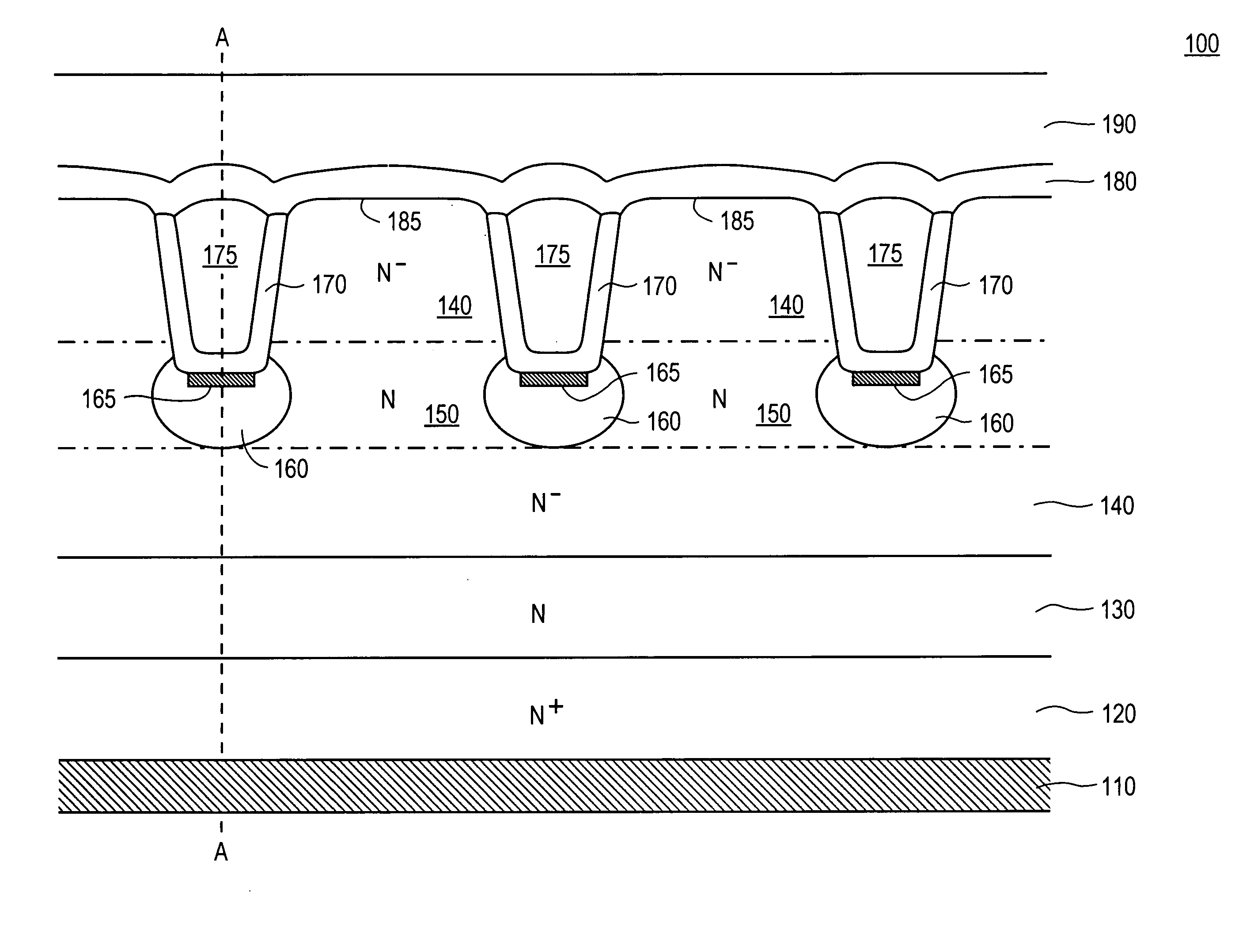
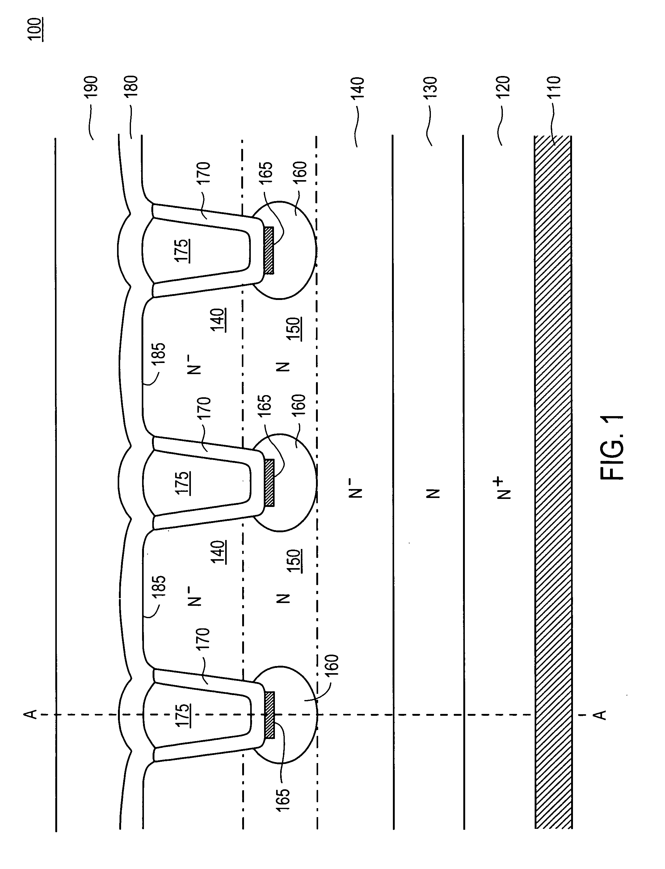
Schottky diodes containing high barrier metal islands in a low barrier metal layer and methods of forming the same
PatentActiveUS7915703B2
Innovation
- A Schottky contact layer with a low barrier metal layer and spaced apart high barrier metal islands is formed on a substrate by controlling the temperature and relative concentrations of high and low barrier metals in a liquid mixture, allowing for the agglomeration of high barrier metal islands while inhibiting the solidification of the low barrier metal, thereby reducing fabrication complexity and improving operational characteristics.


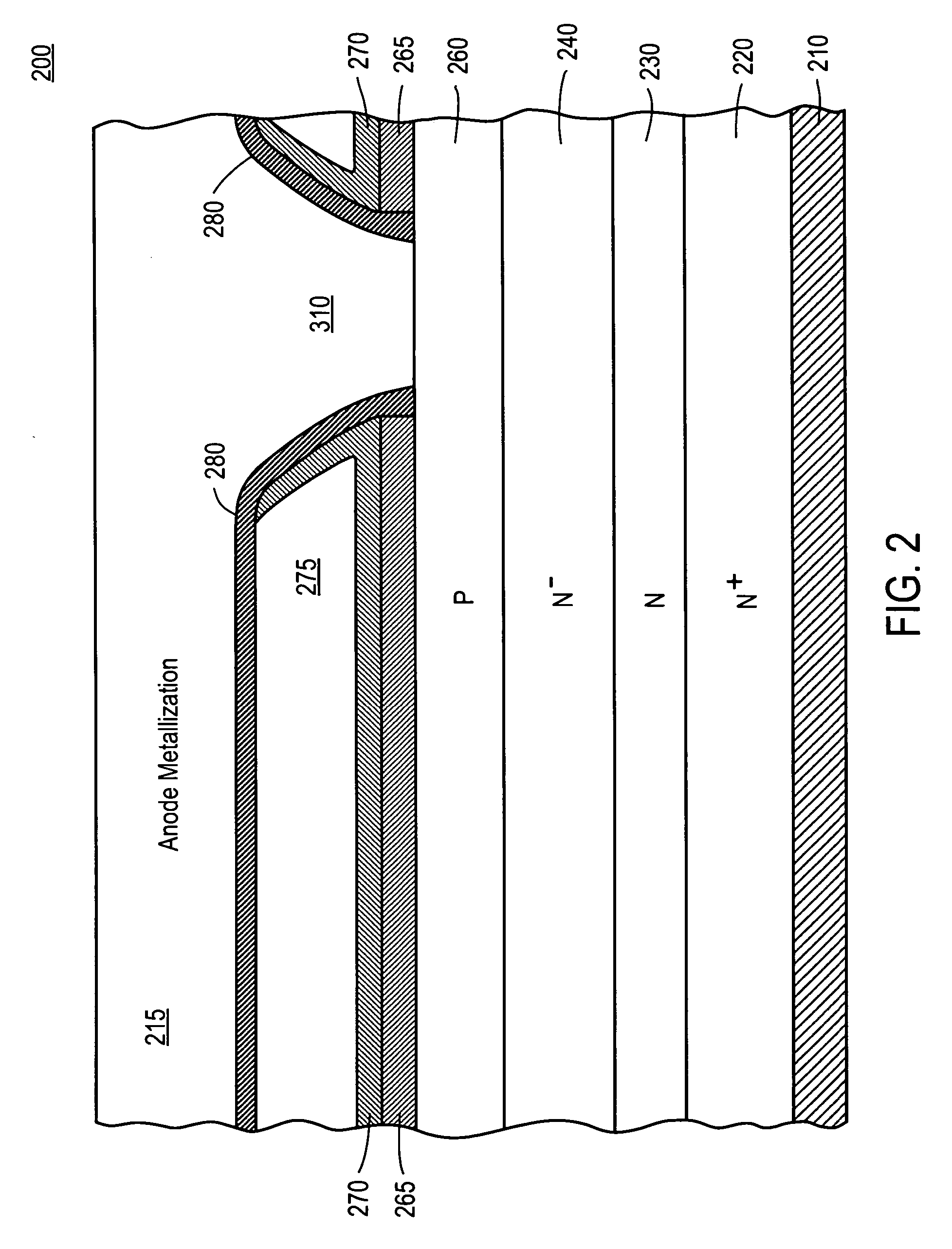
Structure and method for a fast recovery rectifier structure
PatentActiveUS20070145429A1
Innovation
- A fast recovery rectifier structure is developed with a merged PiN Schottky (MPS) diode structure, featuring trenches and oxide layers to reduce reverse recovery charge, while maintaining a soft recovery characteristic, and is fabricated using conventional semiconductor processes, incorporating Schottky diode regions in series with JFET channel regions to enhance the Schottky to PiN ratio and reduce channel resistance.

Energy Efficiency Standards for Power Electronic Devices
The integration of Schottky diodes in fast recovery rectifiers has become increasingly significant in the context of evolving energy efficiency standards for power electronic devices. These standards, established by international organizations such as the International Electrotechnical Commission (IEC) and regional bodies like the European Committee for Electrotechnical Standardization (CENELEC), set stringent requirements for power conversion efficiency, electromagnetic compatibility, and thermal management in electronic systems.
Current energy efficiency standards mandate minimum efficiency thresholds that directly impact the selection and implementation of rectifier technologies. For instance, the IEC 62040 standard for uninterruptible power systems requires efficiency levels exceeding 95% at rated load conditions. Schottky diodes, with their inherently low forward voltage drop typically ranging from 0.2V to 0.45V, provide substantial advantages in meeting these requirements compared to conventional silicon diodes with forward drops of 0.7V to 1.2V.
The IEEE 1547 standard for distributed energy resources interconnection emphasizes rapid response capabilities and minimal power losses during switching operations. Schottky diodes excel in this domain due to their majority carrier conduction mechanism, which eliminates minority carrier storage effects and enables switching speeds in the nanosecond range. This characteristic is particularly valuable in applications requiring compliance with harmonic distortion limits specified in standards such as IEEE 519.
Thermal management requirements outlined in standards like IEC 60747-2 for semiconductor devices impose strict junction temperature limitations and thermal resistance specifications. The superior thermal characteristics of Schottky diodes, combined with their reduced power dissipation, facilitate compliance with these thermal standards while maintaining operational reliability.
Emerging standards for wide bandgap semiconductors, including those developed by JEDEC and SEMI, are establishing new benchmarks for power electronic device performance. Silicon carbide and gallium nitride Schottky diodes are positioned to meet these advanced standards, offering enhanced efficiency and reduced electromagnetic interference compared to traditional silicon-based solutions.
The regulatory landscape continues to evolve with initiatives such as the European Union's Ecodesign Directive, which mandates energy efficiency improvements across various electronic device categories. These regulations drive the adoption of advanced rectifier technologies, positioning Schottky diodes as essential components for achieving compliance while maintaining competitive performance metrics in power electronic applications.
Thermal Management Considerations in High-Speed Rectifiers
Thermal management represents one of the most critical design considerations in high-speed rectifier applications utilizing Schottky diodes. The inherent characteristics of fast recovery rectifiers, particularly their high switching frequencies and substantial current handling capabilities, generate significant heat dissipation challenges that directly impact system reliability and performance.
The primary thermal challenge stems from the power losses occurring during switching transitions and conduction periods. In high-speed rectifier circuits, Schottky diodes experience rapid voltage and current changes, leading to dynamic power dissipation that varies with switching frequency. The forward voltage drop across the diode, typically ranging from 0.3V to 0.7V depending on the specific device characteristics, contributes to steady-state conduction losses that must be effectively managed to prevent junction temperature escalation.
Junction temperature control becomes paramount as excessive heat can degrade the Schottky barrier interface, leading to increased leakage currents and reduced switching performance. The temperature coefficient of Schottky diodes exhibits a negative correlation with forward voltage drop, meaning higher temperatures result in increased conduction losses, creating a potential thermal runaway scenario if inadequately managed.
Effective thermal management strategies encompass multiple approaches, including optimized heat sink design, thermal interface material selection, and PCB layout considerations. Heat sink sizing must account for both steady-state and transient thermal conditions, with particular attention to thermal resistance pathways from junction to ambient. Advanced cooling solutions may incorporate forced air convection or liquid cooling systems for high-power density applications.
PCB thermal design plays a crucial role in heat dissipation, utilizing copper pour techniques, thermal vias, and strategic component placement to create efficient heat conduction paths. The thermal pad design beneath Schottky diode packages requires careful optimization to minimize thermal resistance while maintaining electrical isolation where necessary.
Temperature monitoring and protection circuits become essential components in high-speed rectifier systems, providing real-time thermal feedback to prevent catastrophic failures. These systems can implement dynamic thermal management through switching frequency modulation or load current limiting based on measured junction temperatures, ensuring reliable operation across varying environmental conditions.
Unlock deeper insights with PatSnap Eureka Quick Research — get a full tech report to explore trends and direct your research. Try now!
Generate Your Research Report Instantly with AI Agent
Supercharge your innovation with PatSnap Eureka AI Agent Platform!