

Semiconductor Burn-In and Thermal Design Validation: Key Intersections
MAY 25, 20269 MIN READ
Generate Your Research Report Instantly with AI Agent
PatSnap Eureka helps you evaluate technical feasibility & market potential.
Semiconductor Burn-In and Thermal Validation Background
Semiconductor burn-in testing emerged in the 1960s as a critical reliability assurance methodology, initially developed to address early failure modes in discrete components and simple integrated circuits. The technique was born from the observation that semiconductor devices often exhibit a characteristic "bathtub curve" failure pattern, where failure rates are highest during initial operation periods before stabilizing to lower levels during normal operational life.
The evolution of burn-in practices has been intrinsically linked to thermal management challenges. As semiconductor technology progressed from simple diodes and transistors to complex microprocessors and system-on-chip designs, the thermal stresses imposed during burn-in procedures became increasingly significant. The relationship between elevated temperatures used in accelerated aging and the thermal design validation requirements created a natural convergence point for these two disciplines.
Historical development shows that early burn-in procedures primarily focused on electrical stress testing at elevated temperatures, typically ranging from 125°C to 150°C. However, as device complexity increased and power densities grew exponentially, thermal design validation became equally critical. The intersection point emerged when engineers recognized that burn-in conditions could serve dual purposes: reliability screening and thermal performance validation under extreme conditions.
The technological objectives have evolved to encompass comprehensive validation frameworks that simultaneously address reliability concerns and thermal design adequacy. Modern approaches aim to optimize burn-in parameters not only for defect screening but also for validating thermal management solutions under worst-case scenarios. This dual-purpose methodology enables more efficient validation processes while ensuring both reliability targets and thermal performance specifications are met.
Contemporary goals focus on developing integrated testing methodologies that leverage advanced thermal monitoring and control systems during burn-in procedures. The objective extends beyond traditional pass-fail criteria to include detailed thermal characterization, hotspot identification, and thermal design optimization feedback. This evolution reflects the industry's recognition that thermal and reliability considerations are inseparable in modern semiconductor design validation processes.
The convergence of these disciplines has established new paradigms where thermal design validation and burn-in testing are conducted as complementary processes, sharing infrastructure, methodologies, and data analysis frameworks to achieve comprehensive device qualification objectives.
The evolution of burn-in practices has been intrinsically linked to thermal management challenges. As semiconductor technology progressed from simple diodes and transistors to complex microprocessors and system-on-chip designs, the thermal stresses imposed during burn-in procedures became increasingly significant. The relationship between elevated temperatures used in accelerated aging and the thermal design validation requirements created a natural convergence point for these two disciplines.
Historical development shows that early burn-in procedures primarily focused on electrical stress testing at elevated temperatures, typically ranging from 125°C to 150°C. However, as device complexity increased and power densities grew exponentially, thermal design validation became equally critical. The intersection point emerged when engineers recognized that burn-in conditions could serve dual purposes: reliability screening and thermal performance validation under extreme conditions.
The technological objectives have evolved to encompass comprehensive validation frameworks that simultaneously address reliability concerns and thermal design adequacy. Modern approaches aim to optimize burn-in parameters not only for defect screening but also for validating thermal management solutions under worst-case scenarios. This dual-purpose methodology enables more efficient validation processes while ensuring both reliability targets and thermal performance specifications are met.
Contemporary goals focus on developing integrated testing methodologies that leverage advanced thermal monitoring and control systems during burn-in procedures. The objective extends beyond traditional pass-fail criteria to include detailed thermal characterization, hotspot identification, and thermal design optimization feedback. This evolution reflects the industry's recognition that thermal and reliability considerations are inseparable in modern semiconductor design validation processes.
The convergence of these disciplines has established new paradigms where thermal design validation and burn-in testing are conducted as complementary processes, sharing infrastructure, methodologies, and data analysis frameworks to achieve comprehensive device qualification objectives.
Market Demand for Reliable Semiconductor Testing
The semiconductor industry faces unprecedented pressure to deliver highly reliable components across diverse applications, from consumer electronics to mission-critical aerospace systems. This demand stems from the increasing complexity of integrated circuits and the growing intolerance for field failures in modern electronic systems. As semiconductor devices become more sophisticated and are deployed in safety-critical environments, the market requirement for comprehensive testing methodologies has intensified significantly.
Automotive electronics represents one of the most demanding sectors driving reliable semiconductor testing requirements. The transition toward autonomous vehicles and electric powertrains has elevated the importance of component reliability, where semiconductor failures can have catastrophic consequences. Similarly, the aerospace and defense industries require components that can withstand extreme environmental conditions while maintaining operational integrity over extended periods.
The proliferation of Internet of Things devices has created another substantial market driver for reliable testing solutions. These devices often operate in remote or inaccessible locations where component replacement is costly or impractical. Consequently, manufacturers must ensure exceptional reliability through rigorous testing protocols that can predict long-term performance under various stress conditions.
Data center infrastructure and cloud computing services have emerged as significant consumers of rigorously tested semiconductor components. The economic impact of server failures in these environments has made reliability testing a critical investment priority. Service providers demand components with proven thermal performance and stress tolerance to maintain operational continuity and minimize costly downtime events.
Consumer electronics manufacturers face increasing pressure to reduce warranty costs and maintain brand reputation in competitive markets. This has led to heightened emphasis on burn-in testing and thermal validation processes that can identify potential failures before products reach end users. The cost of field returns and customer dissatisfaction has made comprehensive testing economically justified across various product categories.
The medical device industry represents another growing market segment requiring exceptional semiconductor reliability. Implantable devices and life-support systems demand components with proven long-term stability and predictable failure modes. Regulatory requirements in this sector have established stringent testing standards that drive demand for advanced validation methodologies.
Emerging technologies such as artificial intelligence accelerators and quantum computing components are creating new testing challenges and market opportunities. These applications often involve novel thermal management requirements and stress conditions that traditional testing approaches may not adequately address, necessitating innovative validation techniques.
Automotive electronics represents one of the most demanding sectors driving reliable semiconductor testing requirements. The transition toward autonomous vehicles and electric powertrains has elevated the importance of component reliability, where semiconductor failures can have catastrophic consequences. Similarly, the aerospace and defense industries require components that can withstand extreme environmental conditions while maintaining operational integrity over extended periods.
The proliferation of Internet of Things devices has created another substantial market driver for reliable testing solutions. These devices often operate in remote or inaccessible locations where component replacement is costly or impractical. Consequently, manufacturers must ensure exceptional reliability through rigorous testing protocols that can predict long-term performance under various stress conditions.
Data center infrastructure and cloud computing services have emerged as significant consumers of rigorously tested semiconductor components. The economic impact of server failures in these environments has made reliability testing a critical investment priority. Service providers demand components with proven thermal performance and stress tolerance to maintain operational continuity and minimize costly downtime events.
Consumer electronics manufacturers face increasing pressure to reduce warranty costs and maintain brand reputation in competitive markets. This has led to heightened emphasis on burn-in testing and thermal validation processes that can identify potential failures before products reach end users. The cost of field returns and customer dissatisfaction has made comprehensive testing economically justified across various product categories.
The medical device industry represents another growing market segment requiring exceptional semiconductor reliability. Implantable devices and life-support systems demand components with proven long-term stability and predictable failure modes. Regulatory requirements in this sector have established stringent testing standards that drive demand for advanced validation methodologies.
Emerging technologies such as artificial intelligence accelerators and quantum computing components are creating new testing challenges and market opportunities. These applications often involve novel thermal management requirements and stress conditions that traditional testing approaches may not adequately address, necessitating innovative validation techniques.
Current Burn-In and Thermal Design Challenges
The semiconductor industry faces mounting pressure to deliver increasingly complex chips with higher performance densities while maintaining stringent reliability standards. Current burn-in and thermal design validation processes encounter significant challenges that stem from the fundamental tension between accelerated testing requirements and real-world operational conditions. Traditional burn-in methodologies, developed for simpler semiconductor architectures, struggle to adequately stress modern multi-core processors and system-on-chip designs that generate heterogeneous thermal profiles across different functional blocks.
Thermal gradient management represents one of the most critical challenges in contemporary burn-in operations. Modern semiconductors exhibit non-uniform power dissipation patterns, creating localized hotspots that can exceed safe operating temperatures while other areas remain relatively cool. This thermal heterogeneity complicates the establishment of effective burn-in protocols, as uniform temperature application may either under-stress certain regions or over-stress others, potentially causing premature failures that do not reflect actual usage scenarios.
The integration of advanced packaging technologies, including 3D stacking and chiplet architectures, introduces additional complexity to thermal validation processes. Heat dissipation pathways become increasingly convoluted, making it difficult to predict and control thermal behavior during burn-in testing. Traditional thermal modeling approaches often fail to capture the intricate thermal interactions between multiple die layers or heterogeneous chiplet configurations, leading to inadequate validation coverage.
Power delivery network validation during burn-in presents another significant challenge. Modern semiconductors require precise voltage regulation across multiple power domains, each with distinct current draw characteristics. Burn-in testing must simultaneously validate thermal performance while ensuring power delivery integrity under stress conditions. The dynamic interaction between thermal effects and electrical performance creates complex feedback loops that are difficult to model and validate comprehensively.
Test infrastructure limitations further constrain effective burn-in and thermal validation. Existing burn-in boards and thermal chambers often lack the precision required to create controlled thermal gradients or monitor localized temperature variations with sufficient granularity. The cost and complexity of upgrading test infrastructure to support advanced thermal validation requirements present significant barriers for many semiconductor manufacturers.
Data correlation between burn-in results and field reliability remains problematic. Establishing meaningful relationships between accelerated thermal stress conditions and actual product lifetime performance requires sophisticated statistical models that account for varying operational environments. The challenge intensifies as semiconductor applications expand into automotive, aerospace, and industrial sectors with diverse thermal operating conditions that are difficult to replicate in controlled burn-in environments.
Thermal gradient management represents one of the most critical challenges in contemporary burn-in operations. Modern semiconductors exhibit non-uniform power dissipation patterns, creating localized hotspots that can exceed safe operating temperatures while other areas remain relatively cool. This thermal heterogeneity complicates the establishment of effective burn-in protocols, as uniform temperature application may either under-stress certain regions or over-stress others, potentially causing premature failures that do not reflect actual usage scenarios.
The integration of advanced packaging technologies, including 3D stacking and chiplet architectures, introduces additional complexity to thermal validation processes. Heat dissipation pathways become increasingly convoluted, making it difficult to predict and control thermal behavior during burn-in testing. Traditional thermal modeling approaches often fail to capture the intricate thermal interactions between multiple die layers or heterogeneous chiplet configurations, leading to inadequate validation coverage.
Power delivery network validation during burn-in presents another significant challenge. Modern semiconductors require precise voltage regulation across multiple power domains, each with distinct current draw characteristics. Burn-in testing must simultaneously validate thermal performance while ensuring power delivery integrity under stress conditions. The dynamic interaction between thermal effects and electrical performance creates complex feedback loops that are difficult to model and validate comprehensively.
Test infrastructure limitations further constrain effective burn-in and thermal validation. Existing burn-in boards and thermal chambers often lack the precision required to create controlled thermal gradients or monitor localized temperature variations with sufficient granularity. The cost and complexity of upgrading test infrastructure to support advanced thermal validation requirements present significant barriers for many semiconductor manufacturers.
Data correlation between burn-in results and field reliability remains problematic. Establishing meaningful relationships between accelerated thermal stress conditions and actual product lifetime performance requires sophisticated statistical models that account for varying operational environments. The challenge intensifies as semiconductor applications expand into automotive, aerospace, and industrial sectors with diverse thermal operating conditions that are difficult to replicate in controlled burn-in environments.
Existing Burn-In and Thermal Validation Solutions
01 Burn-in testing systems and methodologies
Systems and methods for conducting burn-in testing of semiconductor devices to identify early failures and ensure reliability. These approaches involve subjecting devices to elevated temperatures and voltages for extended periods to accelerate aging processes and detect potential defects before shipping to customers.- Burn-in testing systems and apparatus: Specialized systems and apparatus designed for conducting burn-in testing of semiconductor devices. These systems provide controlled environments for subjecting semiconductors to elevated temperatures and voltages over extended periods to identify early failures and ensure device reliability. The apparatus typically includes temperature control mechanisms, power supply systems, and monitoring capabilities to track device performance during the burn-in process.
- Thermal management and heat dissipation methods: Techniques and structures for managing heat generation and dissipation during semiconductor burn-in processes. These methods focus on maintaining optimal temperature conditions while preventing overheating that could damage devices or affect test results. Solutions include advanced cooling systems, thermal interface materials, and heat sink designs specifically optimized for burn-in testing environments.
- Temperature monitoring and control systems: Advanced monitoring and control systems that precisely regulate temperature conditions during burn-in testing. These systems employ sensors, feedback mechanisms, and automated control algorithms to maintain consistent thermal conditions across multiple test sites. The technology ensures uniform temperature distribution and provides real-time monitoring capabilities for quality assurance and process optimization.
- Socket and interface design for burn-in testing: Specialized socket designs and electrical interfaces that facilitate reliable connections between semiconductor devices and burn-in test equipment. These designs ensure proper electrical contact, thermal coupling, and mechanical stability during extended testing periods. The interfaces are engineered to handle high temperatures and provide consistent performance across multiple test cycles.
- Validation methodologies and test protocols: Comprehensive validation methodologies and standardized test protocols for evaluating semiconductor reliability through burn-in processes. These approaches define systematic procedures for conducting thermal stress testing, establishing pass/fail criteria, and analyzing test results. The methodologies incorporate statistical analysis techniques and reliability modeling to predict long-term device performance and validate design specifications.
02 Thermal management and heat dissipation solutions
Techniques and apparatus for managing heat generation and dissipation during semiconductor operation and testing. These solutions include heat sinks, thermal interface materials, and cooling systems designed to maintain optimal operating temperatures and prevent thermal damage during high-stress testing conditions.Expand Specific Solutions03 Temperature monitoring and control systems
Systems for precise temperature measurement and control during semiconductor burn-in processes. These technologies enable real-time monitoring of device temperatures and automatic adjustment of testing parameters to maintain desired thermal conditions throughout the validation process.Expand Specific Solutions04 Accelerated aging and stress testing protocols
Methods for implementing accelerated life testing and stress conditions to validate semiconductor reliability within compressed timeframes. These protocols combine thermal, electrical, and mechanical stresses to simulate long-term operating conditions and predict device lifetime performance.Expand Specific Solutions05 Thermal design validation and modeling
Computational and experimental approaches for validating thermal designs of semiconductor packages and systems. These methods include thermal simulation, finite element analysis, and experimental validation techniques to ensure adequate thermal performance under various operating conditions.Expand Specific Solutions
Core Innovations in Integrated Testing Methodologies
Method and apparatus to achieve more level thermal gradient
PatentActiveUS20080147976A1
Innovation
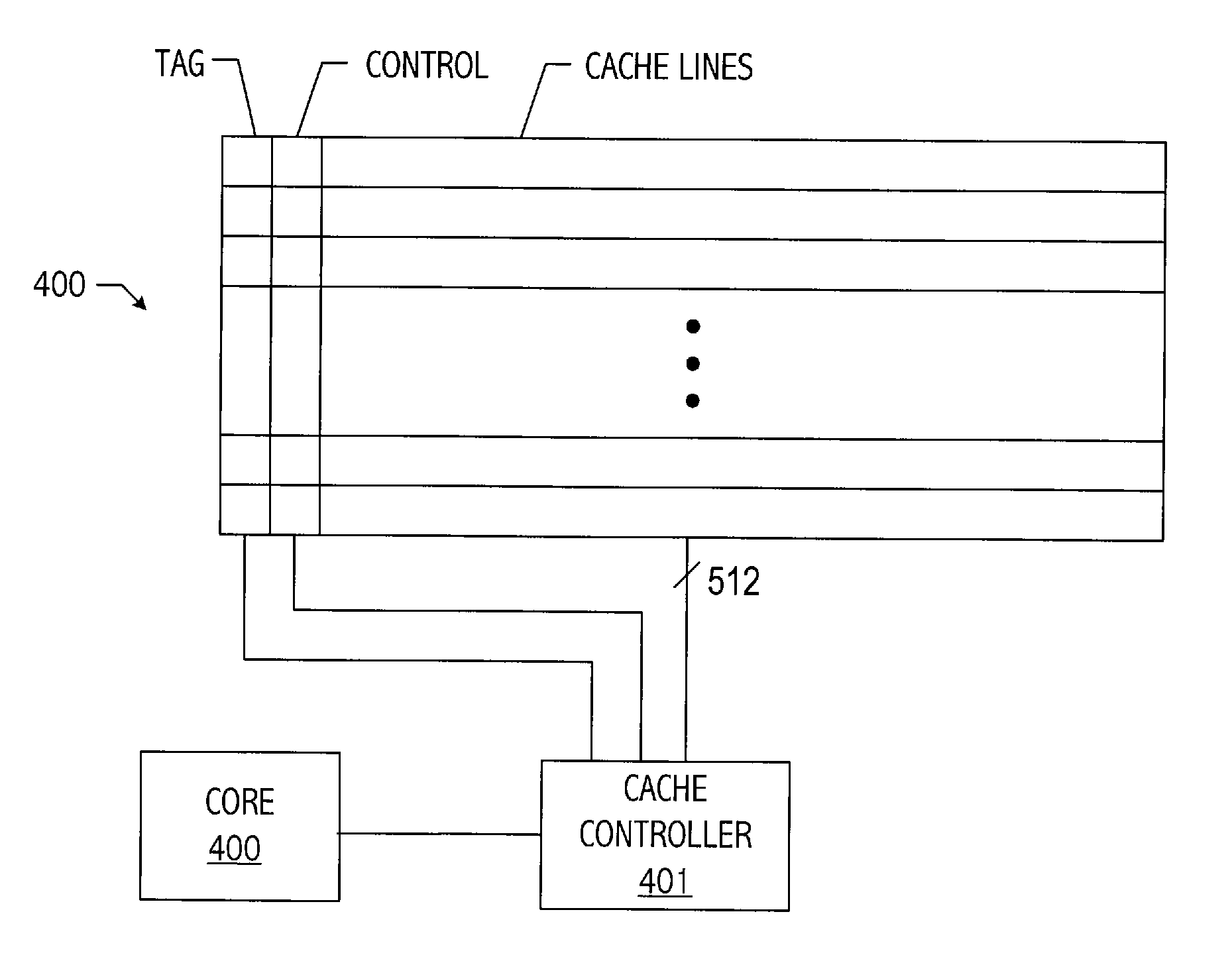
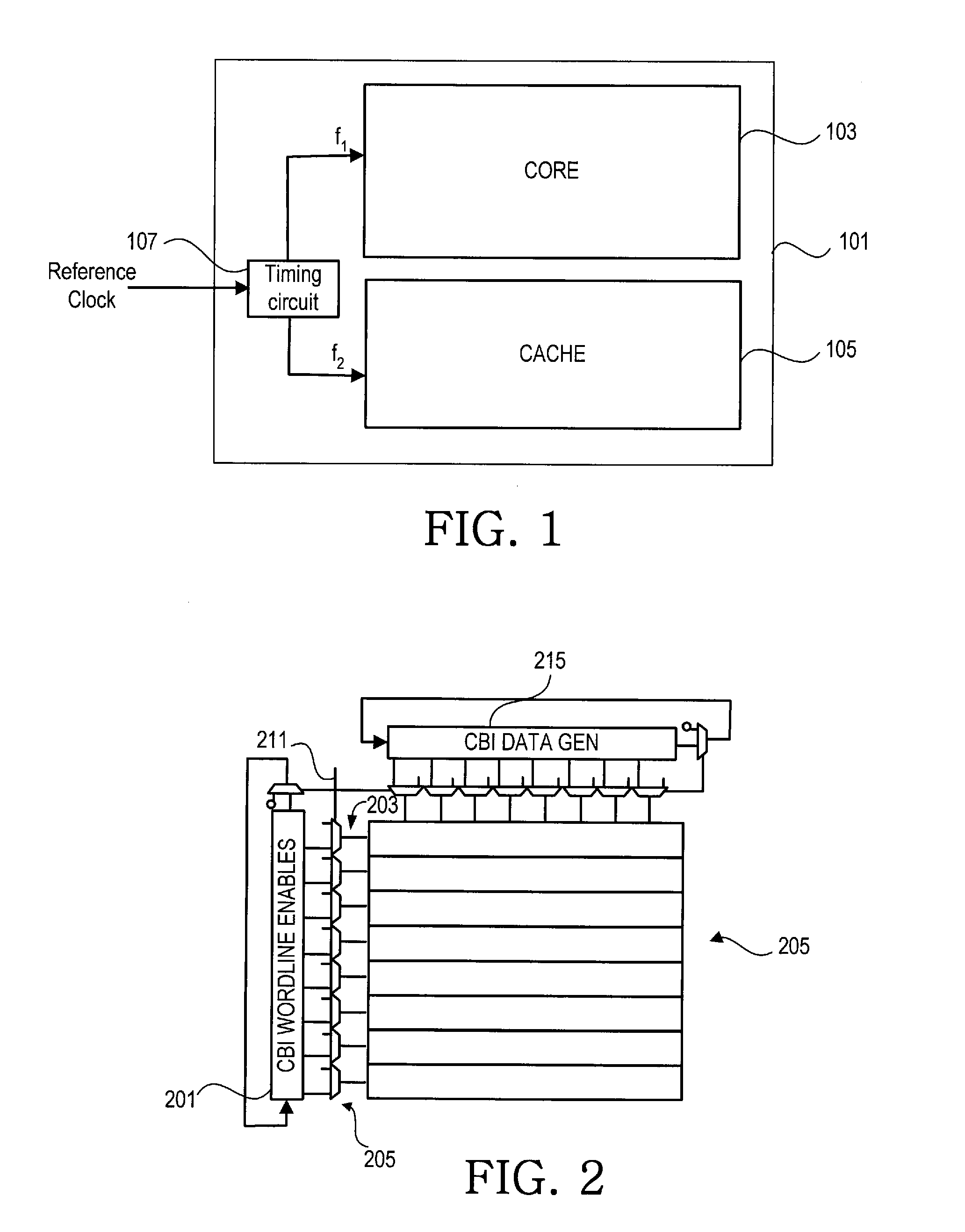
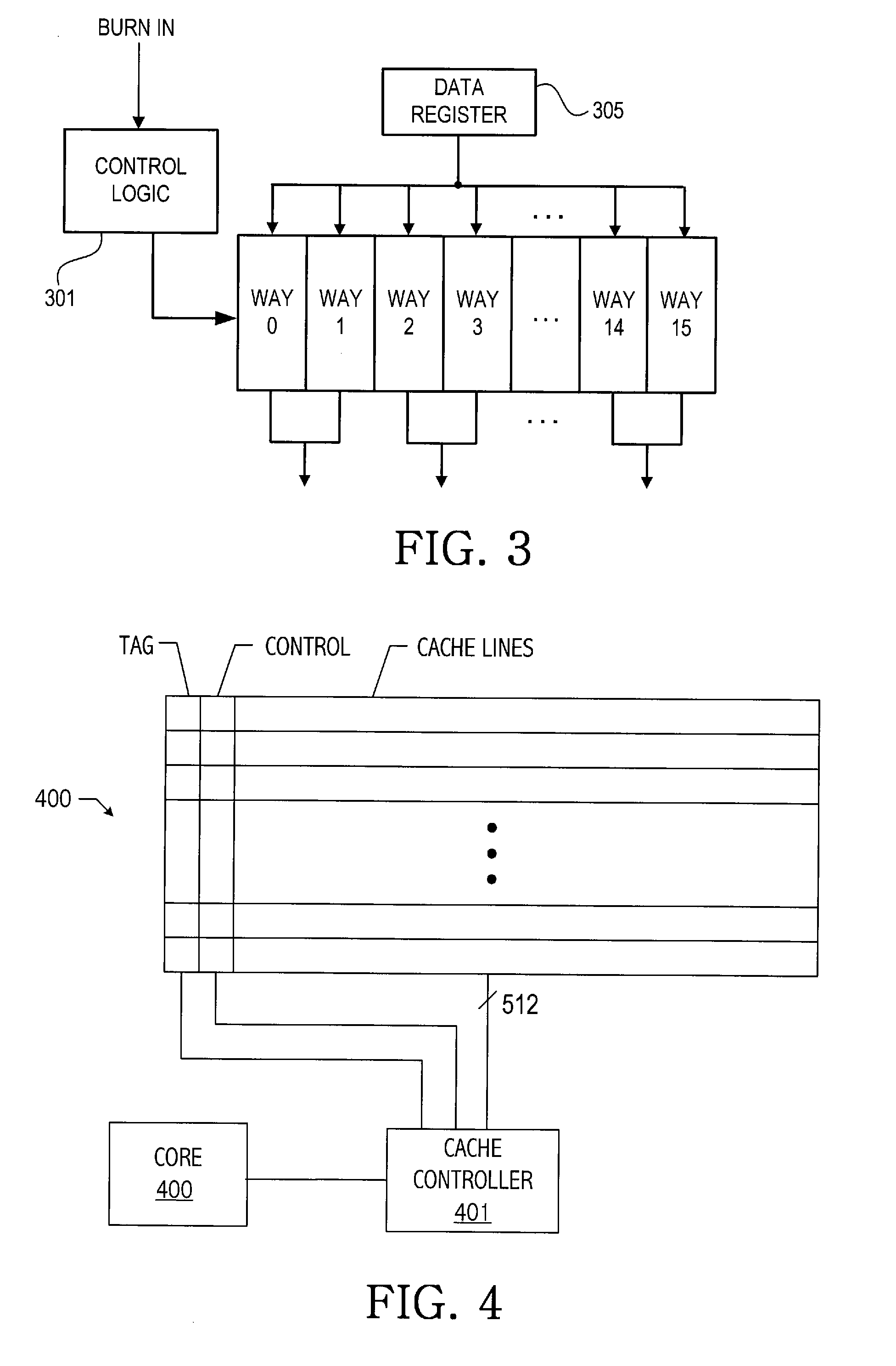
- Increasing cache activity during burn-in by simultaneously accessing multiple memory locations and operating the cache at higher frequencies, while reducing core frequency to achieve more uniform power density and reduce thermal gradients, thereby ensuring all areas of the die are subjected to consistent temperature acceleration.

Semiconductor test device including temperature control module and method of driving the same
PatentActiveUS11927623B2
Innovation
- A semiconductor test device with a chamber, slots, and temperature control modules is introduced, where temperature control modules with inflow and outflow units maintain a consistent temperature across the chamber by mixing and controlling air flow to ensure uniform temperature distribution, thereby ensuring accurate testing of semiconductor devices.


Industry Standards and Compliance Requirements
The semiconductor industry operates under stringent regulatory frameworks that govern burn-in testing and thermal validation processes. These standards ensure product reliability, safety, and performance consistency across global markets. Key international standards include JEDEC specifications, IEC guidelines, and military standards such as MIL-STD-883, which define mandatory testing protocols for semiconductor devices.
JEDEC standards, particularly JESD22 series, establish comprehensive guidelines for environmental stress testing, including burn-in procedures and thermal cycling requirements. These specifications mandate specific temperature profiles, duration parameters, and failure criteria that manufacturers must adhere to during validation processes. The standards also define acceptable thermal resistance values and junction temperature limits for different device categories.
Military and aerospace applications require compliance with MIL-STD-883 and DO-254 standards, which impose more rigorous testing requirements than commercial standards. These specifications demand extended burn-in periods, wider temperature ranges, and enhanced documentation protocols. Defense contractors must demonstrate full traceability and statistical process control throughout the thermal validation lifecycle.
Automotive semiconductor compliance follows AEC-Q100 qualification standards, which integrate burn-in testing with thermal design validation under automotive-specific stress conditions. These requirements address unique challenges such as under-hood temperature extremes, thermal shock resistance, and long-term reliability over vehicle lifespans exceeding 15 years.
Regional regulatory bodies impose additional compliance layers. The European Union's RoHS and REACH regulations affect material selection and testing methodologies, while FCC requirements in the United States mandate electromagnetic compatibility validation during thermal stress testing. Asian markets, particularly Japan and South Korea, maintain specific quality standards that influence burn-in protocols and thermal characterization procedures.
Emerging compliance trends focus on sustainability and energy efficiency requirements. New standards increasingly emphasize thermal management optimization to reduce power consumption and environmental impact, driving innovation in both burn-in methodologies and thermal design validation approaches across the semiconductor industry.
JEDEC standards, particularly JESD22 series, establish comprehensive guidelines for environmental stress testing, including burn-in procedures and thermal cycling requirements. These specifications mandate specific temperature profiles, duration parameters, and failure criteria that manufacturers must adhere to during validation processes. The standards also define acceptable thermal resistance values and junction temperature limits for different device categories.
Military and aerospace applications require compliance with MIL-STD-883 and DO-254 standards, which impose more rigorous testing requirements than commercial standards. These specifications demand extended burn-in periods, wider temperature ranges, and enhanced documentation protocols. Defense contractors must demonstrate full traceability and statistical process control throughout the thermal validation lifecycle.
Automotive semiconductor compliance follows AEC-Q100 qualification standards, which integrate burn-in testing with thermal design validation under automotive-specific stress conditions. These requirements address unique challenges such as under-hood temperature extremes, thermal shock resistance, and long-term reliability over vehicle lifespans exceeding 15 years.
Regional regulatory bodies impose additional compliance layers. The European Union's RoHS and REACH regulations affect material selection and testing methodologies, while FCC requirements in the United States mandate electromagnetic compatibility validation during thermal stress testing. Asian markets, particularly Japan and South Korea, maintain specific quality standards that influence burn-in protocols and thermal characterization procedures.
Emerging compliance trends focus on sustainability and energy efficiency requirements. New standards increasingly emphasize thermal management optimization to reduce power consumption and environmental impact, driving innovation in both burn-in methodologies and thermal design validation approaches across the semiconductor industry.
Cost-Effectiveness Analysis of Testing Strategies
The cost-effectiveness analysis of semiconductor burn-in and thermal design validation testing strategies requires a comprehensive evaluation framework that balances testing thoroughness with economic constraints. Traditional burn-in testing, while highly effective at identifying early-life failures, represents a significant cost burden due to extended test durations, energy consumption, and equipment utilization. The challenge lies in optimizing testing protocols to maintain reliability standards while minimizing overall testing expenditure.
Statistical sampling approaches offer substantial cost reduction opportunities compared to 100% burn-in testing. By implementing risk-based sampling methodologies, manufacturers can achieve comparable defect detection rates while testing only a representative subset of production volumes. Advanced statistical models, including Weibull analysis and accelerated life testing principles, enable precise determination of optimal sample sizes based on acceptable quality levels and confidence intervals.
Accelerated thermal testing presents another cost-effective alternative to traditional burn-in procedures. By elevating temperature stress levels beyond normal operating conditions, test durations can be significantly reduced while maintaining equivalent failure detection capabilities. The Arrhenius equation provides the theoretical foundation for establishing acceleration factors, enabling manufacturers to compress weeks of traditional burn-in into hours of accelerated testing.
Hybrid testing strategies demonstrate superior cost-effectiveness by combining multiple validation approaches. Initial screening using rapid thermal cycling can identify gross defects, followed by targeted burn-in testing for critical applications or high-risk product categories. This tiered approach optimizes resource allocation while maintaining comprehensive coverage of potential failure mechanisms.
Economic modeling reveals that optimal testing strategies vary significantly based on product complexity, target markets, and failure cost implications. High-reliability applications justify extensive testing investments due to catastrophic failure consequences, while consumer electronics benefit from streamlined validation protocols focused on dominant failure modes. Return on investment calculations must incorporate not only direct testing costs but also warranty expenses, field failure impacts, and brand reputation considerations.
Emerging technologies including machine learning-based predictive analytics and real-time thermal monitoring systems offer promising avenues for further cost optimization. These approaches enable dynamic adjustment of testing parameters based on real-time performance indicators, potentially reducing testing requirements while enhancing defect detection accuracy through intelligent pattern recognition algorithms.
Statistical sampling approaches offer substantial cost reduction opportunities compared to 100% burn-in testing. By implementing risk-based sampling methodologies, manufacturers can achieve comparable defect detection rates while testing only a representative subset of production volumes. Advanced statistical models, including Weibull analysis and accelerated life testing principles, enable precise determination of optimal sample sizes based on acceptable quality levels and confidence intervals.
Accelerated thermal testing presents another cost-effective alternative to traditional burn-in procedures. By elevating temperature stress levels beyond normal operating conditions, test durations can be significantly reduced while maintaining equivalent failure detection capabilities. The Arrhenius equation provides the theoretical foundation for establishing acceleration factors, enabling manufacturers to compress weeks of traditional burn-in into hours of accelerated testing.
Hybrid testing strategies demonstrate superior cost-effectiveness by combining multiple validation approaches. Initial screening using rapid thermal cycling can identify gross defects, followed by targeted burn-in testing for critical applications or high-risk product categories. This tiered approach optimizes resource allocation while maintaining comprehensive coverage of potential failure mechanisms.
Economic modeling reveals that optimal testing strategies vary significantly based on product complexity, target markets, and failure cost implications. High-reliability applications justify extensive testing investments due to catastrophic failure consequences, while consumer electronics benefit from streamlined validation protocols focused on dominant failure modes. Return on investment calculations must incorporate not only direct testing costs but also warranty expenses, field failure impacts, and brand reputation considerations.
Emerging technologies including machine learning-based predictive analytics and real-time thermal monitoring systems offer promising avenues for further cost optimization. These approaches enable dynamic adjustment of testing parameters based on real-time performance indicators, potentially reducing testing requirements while enhancing defect detection accuracy through intelligent pattern recognition algorithms.
Unlock deeper insights with PatSnap Eureka Quick Research — get a full tech report to explore trends and direct your research. Try now!
Generate Your Research Report Instantly with AI Agent
Supercharge your innovation with PatSnap Eureka AI Agent Platform!