

Semiconductor Burn-In Procedures for Edge Computing Applications
MAY 25, 20269 MIN READ
Generate Your Research Report Instantly with AI Agent
PatSnap Eureka helps you evaluate technical feasibility & market potential.
Semiconductor Burn-In Background and Edge Computing Goals
Semiconductor burn-in procedures have evolved as a critical quality assurance methodology since the early days of integrated circuit manufacturing in the 1960s. Originally developed to address infant mortality failures in electronic components, burn-in testing involves subjecting semiconductor devices to elevated temperature and voltage stress conditions for extended periods. This process accelerates potential failure mechanisms, allowing defective units to fail during manufacturing rather than in field deployment.
The fundamental principle behind burn-in testing relies on the bathtub curve failure distribution model, where electronic components exhibit higher failure rates during initial operation periods before stabilizing into their useful life phase. Traditional burn-in procedures typically involve exposing devices to temperatures ranging from 125°C to 150°C while applying operational or elevated voltages for durations spanning 48 to 168 hours, depending on device complexity and reliability requirements.
Edge computing represents a paradigm shift in computational architecture, bringing processing capabilities closer to data sources and end users. Unlike centralized cloud computing models, edge computing distributes computational resources across numerous nodes positioned at network peripheries. This distributed approach enables real-time data processing, reduces latency, and minimizes bandwidth requirements for applications requiring immediate response capabilities.
The convergence of semiconductor reliability requirements with edge computing deployment scenarios creates unique challenges and opportunities. Edge computing applications demand unprecedented reliability levels due to their distributed nature and often inaccessible deployment locations. Devices deployed in autonomous vehicles, industrial IoT sensors, smart city infrastructure, and remote monitoring systems cannot afford unexpected failures that might compromise safety or operational continuity.
Current edge computing goals emphasize achieving ultra-low latency processing, typically targeting sub-millisecond response times for critical applications. Power efficiency remains paramount, as many edge devices operate on battery power or have limited energy budgets. Additionally, edge computing systems must demonstrate exceptional reliability over extended operational periods, often exceeding traditional consumer electronics expectations.
The integration of advanced semiconductor technologies, including system-on-chip designs, neuromorphic processors, and specialized AI accelerators, into edge computing platforms necessitates refined burn-in methodologies. These sophisticated devices incorporate multiple functional blocks, heterogeneous processing elements, and complex interconnect structures that require comprehensive stress testing to ensure field reliability.
Modern edge computing applications also introduce new environmental stress factors that traditional burn-in procedures may not adequately address. Devices must withstand temperature cycling, vibration, humidity variations, and electromagnetic interference while maintaining consistent performance across diverse deployment scenarios.
Market Demand for Reliable Edge Computing Semiconductors
The global edge computing market is experiencing unprecedented growth driven by the proliferation of Internet of Things devices, autonomous vehicles, industrial automation systems, and real-time data processing requirements. This expansion directly translates into heightened demand for semiconductors that can operate reliably in distributed computing environments where traditional data center infrastructure is impractical or insufficient.
Edge computing applications impose unique reliability requirements on semiconductor components due to their deployment in harsh and uncontrolled environments. Unlike data center processors that operate in climate-controlled facilities with redundant power supplies and maintenance teams, edge semiconductors must function autonomously in industrial settings, outdoor installations, and mobile platforms where temperature fluctuations, vibration, and power instabilities are common.
The automotive sector represents a particularly demanding segment where semiconductor reliability is paramount. Advanced driver assistance systems and autonomous driving technologies require processors that maintain consistent performance across extreme temperature ranges while processing safety-critical computations in real-time. Similarly, industrial IoT applications in manufacturing, oil and gas, and smart infrastructure demand semiconductors capable of continuous operation for years without maintenance intervention.
Telecommunications infrastructure supporting 5G networks and edge data centers requires semiconductors with exceptional mean time between failure rates. Network operators cannot afford component failures that could disrupt service to thousands of users or compromise network security. The distributed nature of edge computing means that failed components are often difficult and expensive to replace, making initial reliability investments more cost-effective than field replacements.
Smart city initiatives and environmental monitoring systems further drive demand for ultra-reliable semiconductors. These applications often involve remote sensor networks and processing nodes deployed in challenging outdoor conditions where component access is limited and environmental stresses are severe.
The market increasingly values semiconductors that have undergone rigorous burn-in testing procedures specifically designed for edge computing stress profiles. Traditional burn-in methods developed for consumer electronics or data center applications may not adequately simulate the unique operational stresses encountered in edge deployments, creating opportunities for specialized testing methodologies that better predict long-term reliability in distributed computing environments.
Current Burn-In Challenges for Edge Computing Chips
Edge computing chips face unprecedented burn-in challenges due to their unique operational requirements and deployment environments. Unlike traditional data center processors that operate in controlled conditions, edge computing semiconductors must withstand extreme temperature variations, humidity fluctuations, and mechanical stress while maintaining consistent performance across diverse geographical locations.
The heterogeneous nature of edge computing workloads presents significant testing complexities. These chips must handle artificial intelligence inference, real-time data processing, and communication protocols simultaneously, requiring burn-in procedures that can accurately simulate such diverse computational demands. Traditional burn-in methods designed for single-purpose processors prove inadequate for validating the reliability of multi-functional edge computing architectures.
Power management emerges as a critical challenge during burn-in testing. Edge devices operate under strict power constraints, often relying on battery power or limited energy harvesting systems. Burn-in procedures must therefore validate power efficiency across various operational modes while ensuring thermal stability under constrained cooling conditions. This requirement conflicts with traditional high-stress burn-in approaches that typically consume maximum power.
Miniaturization trends in edge computing create additional complications for burn-in testing infrastructure. Advanced packaging technologies such as system-in-package and 3D integration make it difficult to access individual components for monitoring during burn-in. The increased integration density also amplifies thermal management challenges, as heat dissipation becomes more complex in compact form factors.
The distributed nature of edge computing deployments demands accelerated burn-in methodologies. Unlike centralized systems where field failures can be quickly addressed, edge devices often operate in remote or inaccessible locations. This reality necessitates more rigorous burn-in procedures to prevent field failures, yet time-to-market pressures limit the duration available for comprehensive testing.
Security considerations add another layer of complexity to burn-in procedures. Edge computing chips increasingly incorporate hardware security modules and cryptographic accelerators that require specialized validation during burn-in. These security features must be tested under stress conditions without compromising their integrity or revealing sensitive information about their implementation.
Existing Burn-In Solutions for Edge Computing Applications
01 Burn-in test equipment and apparatus design
Specialized equipment and apparatus are designed for conducting burn-in tests on semiconductor devices. These systems provide controlled environments with precise temperature, voltage, and timing controls to stress test semiconductor components. The equipment includes test sockets, heating chambers, and monitoring systems to ensure proper burn-in conditions are maintained throughout the testing process.- Temperature control and thermal management in burn-in testing: Semiconductor burn-in procedures require precise temperature control and thermal management systems to subject devices to elevated temperatures for extended periods. These systems ensure uniform heat distribution across test chambers and maintain stable thermal conditions throughout the burn-in process. Advanced thermal management techniques help identify temperature-sensitive defects and improve device reliability by simulating operational stress conditions.
- Automated burn-in test equipment and apparatus: Automated burn-in systems incorporate sophisticated test equipment and apparatus designed to handle multiple semiconductor devices simultaneously. These systems feature programmable test sequences, automated device handling mechanisms, and real-time monitoring capabilities. The equipment enables efficient high-volume testing while reducing manual intervention and improving test consistency across different device types.
- Electrical stress application and voltage management: Burn-in procedures involve applying controlled electrical stress to semiconductor devices through precise voltage and current management systems. These methods subject devices to operating conditions that accelerate potential failure mechanisms, allowing early detection of defective components. The electrical stress protocols are carefully designed to simulate real-world operating conditions while maintaining device integrity.
- Socket and interface technologies for device connection: Specialized socket and interface technologies provide reliable electrical connections between semiconductor devices and burn-in test systems. These connection methods ensure proper signal transmission and power delivery during extended test periods. Advanced socket designs accommodate various package types and maintain consistent contact pressure throughout the burn-in process, preventing connection failures that could affect test results.
- Process monitoring and failure analysis methods: Comprehensive monitoring and analysis methods track device performance parameters throughout the burn-in process to identify failure patterns and optimize test procedures. These techniques include real-time data collection, statistical analysis of failure rates, and correlation of test conditions with device behavior. Advanced monitoring systems enable early detection of anomalies and provide valuable feedback for improving manufacturing processes.
02 Temperature control and thermal management during burn-in
Temperature control is critical in semiconductor burn-in procedures to ensure devices are subjected to appropriate thermal stress. Systems incorporate heating elements, temperature sensors, and thermal management solutions to maintain uniform temperature distribution across test devices. Proper thermal cycling and temperature ramping procedures help identify temperature-sensitive defects in semiconductor components.Expand Specific Solutions03 Electrical stress testing and voltage application methods
Electrical stress testing involves applying specific voltage and current conditions to semiconductor devices during burn-in to accelerate potential failure mechanisms. Various voltage application methods and electrical stress patterns are employed to simulate long-term operational conditions in a compressed timeframe. These procedures help identify electrically sensitive defects and ensure device reliability under normal operating conditions.Expand Specific Solutions04 Burn-in process optimization and time management
Optimization of burn-in procedures involves determining appropriate test durations, stress levels, and process parameters to maximize defect detection while minimizing test time and costs. Process optimization includes statistical analysis of failure rates, development of accelerated test methods, and implementation of adaptive burn-in strategies based on device characteristics and quality requirements.Expand Specific Solutions05 Monitoring and data collection systems for burn-in testing
Advanced monitoring and data collection systems are implemented to track device performance during burn-in procedures. These systems continuously monitor electrical parameters, temperature conditions, and failure events to provide real-time feedback on test progress. Data analysis capabilities enable identification of failure patterns, process improvements, and quality assessment of semiconductor devices throughout the burn-in process.Expand Specific Solutions
Key Players in Edge Computing Semiconductor Testing
The semiconductor burn-in procedures for edge computing applications market is experiencing rapid growth driven by the increasing deployment of edge computing infrastructure across industries. The market is in an expansion phase, with significant investments in specialized testing equipment to ensure reliability of semiconductors operating in harsh edge environments. Major semiconductor manufacturers like Intel Corp., Micron Technology, Texas Instruments, and Renesas Electronics are driving technology advancement, while specialized test equipment providers such as Aehr Test Systems, Advantest Corp., FormFactor Inc., and Applied Materials are developing sophisticated burn-in solutions. The technology maturity varies across segments, with established players like Lam Research and Varian Semiconductor offering proven solutions, while emerging companies focus on edge-specific requirements. Asian manufacturers including Toshiba, Mitsubishi Electric, and Chinese firms like Wuhan Jingce are expanding capabilities to meet growing regional demand for edge computing semiconductor testing.
Intel Corp.
Technical Solution: Intel has developed comprehensive burn-in procedures specifically optimized for edge computing semiconductors, focusing on accelerated aging tests under elevated temperature and voltage stress conditions. Their approach incorporates dynamic burn-in methodologies that simulate real-world edge computing workloads, including intermittent processing bursts and power cycling scenarios typical in IoT devices. Intel's burn-in protocols utilize specialized test patterns that stress both logic and memory components simultaneously, ensuring reliability in resource-constrained edge environments. The company has implemented adaptive burn-in duration based on target application requirements, with shorter cycles for consumer edge devices and extended procedures for industrial applications. Their methodology includes comprehensive parametric monitoring during burn-in to identify early failure mechanisms specific to edge computing stress patterns.
Strengths: Industry-leading experience in processor burn-in, comprehensive test coverage for complex SoCs, established reliability standards. Weaknesses: Higher cost procedures, longer burn-in cycles may impact time-to-market for edge applications.
Texas Instruments Incorporated
Technical Solution: TI has developed specialized burn-in procedures tailored for their extensive portfolio of edge computing semiconductors, particularly focusing on mixed-signal devices and microcontrollers used in IoT applications. Their burn-in methodology emphasizes thermal cycling combined with functional testing to ensure reliability in harsh edge environments. TI's approach includes accelerated life testing protocols that simulate years of operation in compressed timeframes, utilizing elevated temperatures up to 150°C and voltage stress conditions. The company has implemented automated burn-in systems that can handle high-volume production while maintaining statistical process control. Their procedures specifically address power management ICs and sensor interface circuits critical for edge computing applications, incorporating real-time monitoring of key parameters during the burn-in process to optimize yield and reliability.
Strengths: Extensive experience with mixed-signal devices, cost-effective burn-in solutions, strong focus on automotive and industrial reliability standards. Weaknesses: Limited to specific device categories, may require customization for advanced edge computing processors.
Core Innovations in Edge Computing Burn-In Procedures
Wafer holder, heater unit having the wafer holder, and wafer prober having the heater unit
PatentInactiveUS20070082313A1
Innovation
- A wafer holder design featuring a chuck top with a conductive layer and a supporter, where a space is formed between them, and a support member is inserted to reduce deformation and improve heat insulation, using materials with matching thermal expansion coefficients and high Young's modulus, such as mullite-alumina composites, to enhance rigidity and thermal management.

Method and apparatus for burn-in of semiconductor devices
PatentInactiveUS7275188B1
Innovation
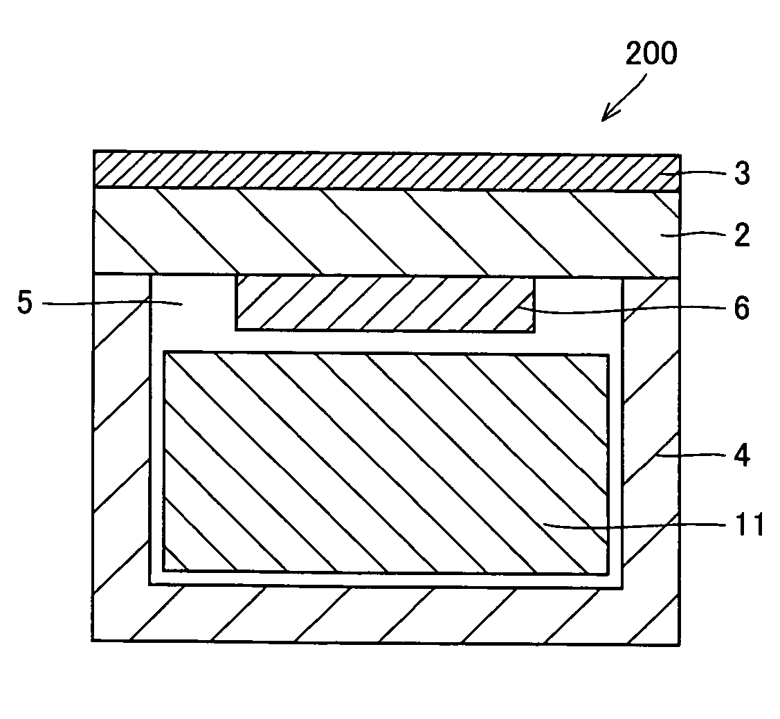
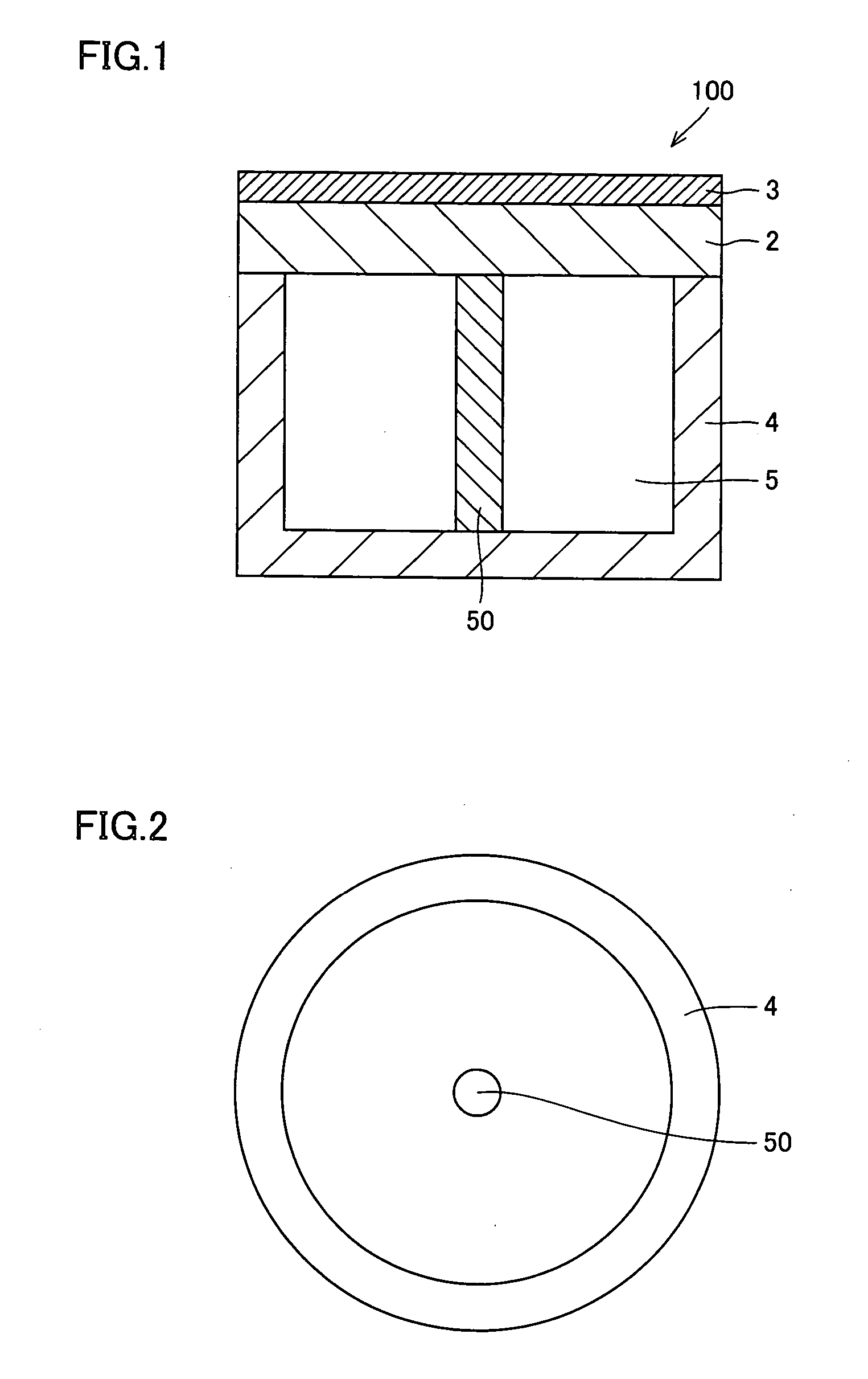
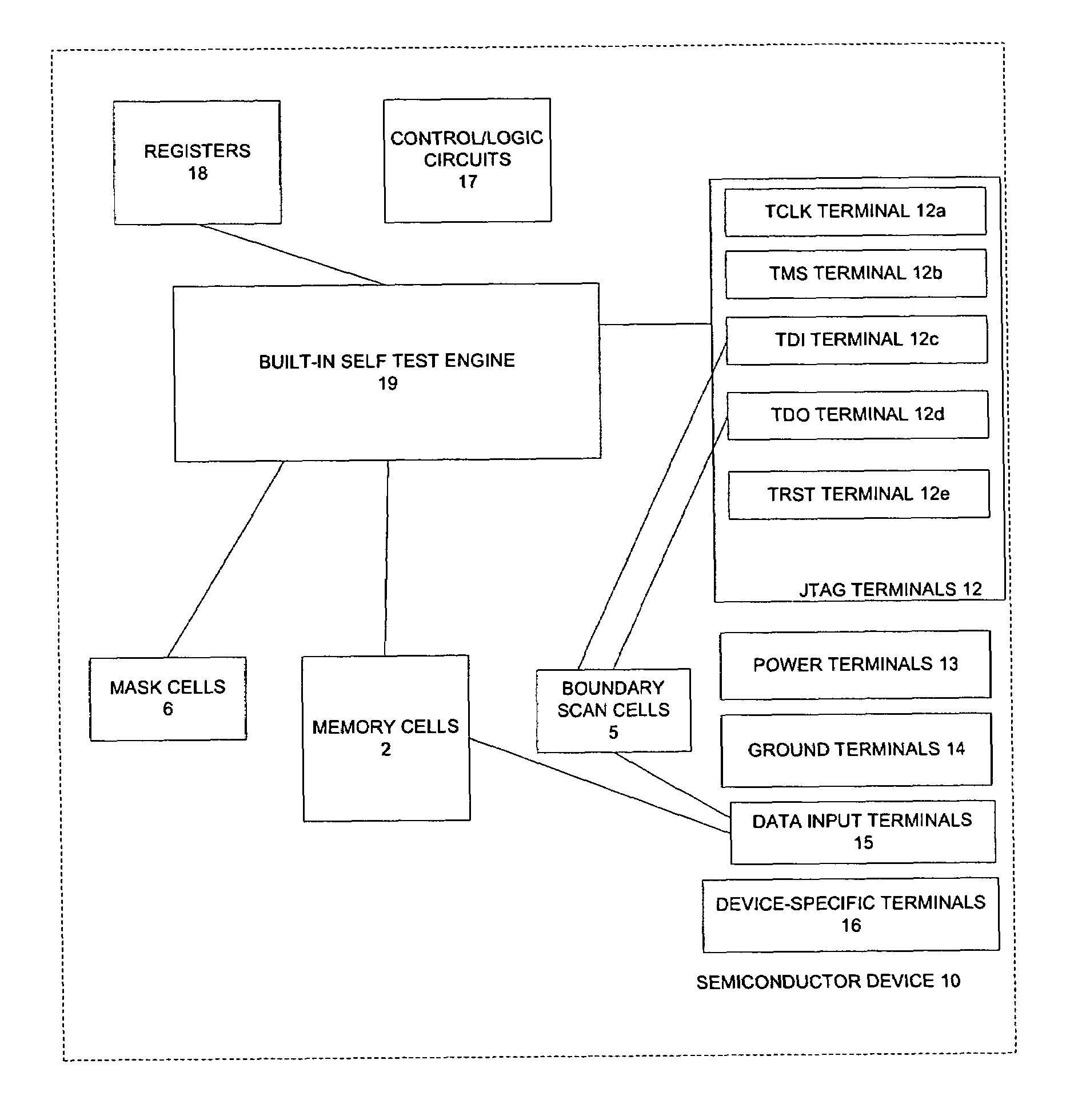
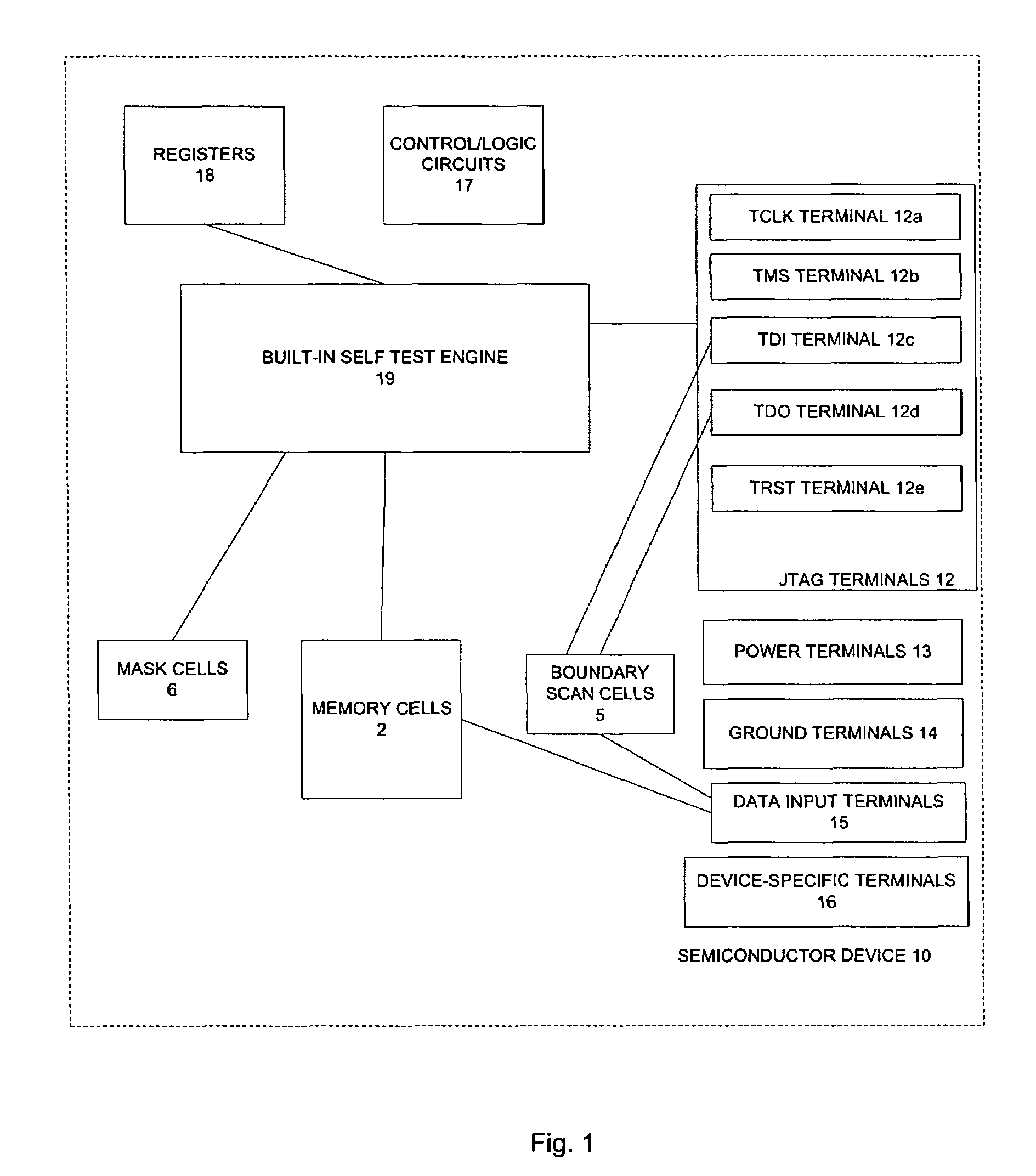
- A method and apparatus that utilize a reduced pin-count socket and JTAG terminals to perform burn-in operations, eliminating the need for data transmission through data input terminals, allowing for efficient burn-in of semiconductor devices with large memory arrays using built-in self-test circuitry and serial data transfer via JTAG terminals.

Quality Standards for Edge Computing Semiconductor Testing
Edge computing semiconductor testing requires adherence to stringent quality standards that differ significantly from traditional data center applications. The unique operational environment of edge devices, characterized by distributed deployment, limited maintenance access, and diverse environmental conditions, necessitates specialized testing protocols that ensure long-term reliability and performance consistency.
International standards organizations have established comprehensive frameworks for edge computing semiconductor quality assurance. IEC 62899 series provides fundamental guidelines for semiconductor device reliability in distributed computing environments, while JEDEC standards JESD47 and JESD22 define specific test methodologies for stress testing and environmental qualification. These standards emphasize accelerated aging tests, thermal cycling protocols, and electromagnetic compatibility requirements tailored to edge deployment scenarios.
Military and automotive quality standards significantly influence edge computing semiconductor testing due to similar harsh operating conditions. MIL-STD-883 and AEC-Q100 qualification procedures have been adapted for edge applications, incorporating extended temperature ranges, vibration resistance, and humidity tolerance specifications. These adaptations recognize that edge devices often operate in uncontrolled environments similar to automotive or military applications.
Functional testing standards for edge semiconductors focus on real-time performance validation under varying computational loads. IEEE 1149.1 boundary scan testing ensures comprehensive fault detection, while application-specific performance benchmarks validate processing capabilities under typical edge workloads. Power consumption testing follows strict efficiency standards, as edge devices frequently operate under power constraints that demand optimal energy utilization.
Quality assurance protocols mandate statistical sampling methodologies and defect rate thresholds specifically calibrated for edge computing reliability requirements. Zero-defect policies are often implemented for critical edge applications, requiring 100% functional testing and burn-in validation. Traceability standards ensure complete documentation of testing procedures, environmental conditions, and performance metrics throughout the qualification process.
Emerging quality standards address cybersecurity and data integrity concerns unique to edge computing environments. Hardware security module testing, secure boot validation, and cryptographic performance verification have become integral components of comprehensive quality assurance frameworks, ensuring edge semiconductors meet both performance and security requirements essential for distributed computing applications.
Cost-Effectiveness Analysis of Edge Computing Burn-In
The cost-effectiveness analysis of edge computing burn-in procedures presents a complex economic evaluation framework that balances initial testing investments against long-term operational benefits. Traditional burn-in processes, while effective at identifying early-life failures, introduce significant upfront costs that must be carefully weighed against the unique operational requirements of edge computing deployments.
Edge computing applications operate in distributed environments where device accessibility and replacement costs differ substantially from centralized data center scenarios. The economic model must account for higher field service costs, extended downtime impacts, and the cascading effects of device failures on edge network performance. These factors fundamentally alter the cost-benefit equation compared to traditional semiconductor applications.
Initial burn-in investments typically range from 15-30% of device manufacturing costs, depending on test duration and complexity. However, edge computing deployments can justify higher burn-in investments due to elevated field replacement costs, which often exceed 3-5 times the original device cost when factoring in logistics, technician deployment, and service disruption.
The analysis reveals that accelerated burn-in procedures optimized for edge computing can achieve break-even points within 18-24 months of deployment. Key cost drivers include reduced warranty claims, minimized field service interventions, and improved system availability metrics. Edge applications with high uptime requirements demonstrate particularly favorable economics, with some scenarios showing 200-300% return on burn-in investment over a three-year operational period.
Risk mitigation benefits provide additional economic value through reduced liability exposure and enhanced service level agreement compliance. Edge computing customers increasingly demand stringent reliability guarantees, making comprehensive burn-in procedures a competitive differentiator rather than merely a cost center.
The economic optimization model suggests that selective burn-in strategies, targeting high-risk device populations and critical deployment scenarios, can maximize cost-effectiveness while maintaining reliability objectives. This approach enables manufacturers to balance testing thoroughness with economic constraints in price-sensitive edge computing markets.
Unlock deeper insights with PatSnap Eureka Quick Research — get a full tech report to explore trends and direct your research. Try now!
Generate Your Research Report Instantly with AI Agent
Supercharge your innovation with PatSnap Eureka AI Agent Platform!