

Solve Layered Warpage Affecting Wire Sweep In PCB Design
MAY 27, 20268 MIN READ
Generate Your Research Report Instantly with AI Agent
PatSnap Eureka helps you evaluate technical feasibility & market potential.
PCB Warpage Control Background and Design Objectives
Printed Circuit Board (PCB) warpage has emerged as a critical challenge in modern electronics manufacturing, particularly as devices continue to miniaturize while demanding higher performance and reliability. The phenomenon of layered warpage occurs when differential thermal expansion, moisture absorption, and mechanical stresses cause non-uniform deformation across PCB layers during manufacturing processes such as reflow soldering, wave soldering, and thermal cycling operations.
Wire sweep, a related manufacturing defect, manifests when bond wires connecting semiconductor dies to lead frames or substrates are displaced from their intended positions due to molding compound flow during encapsulation processes. The intersection of these two phenomena creates a compounding effect where PCB warpage-induced mechanical stresses exacerbate wire sweep tendencies, leading to electrical failures, reduced product reliability, and increased manufacturing costs.
The evolution of PCB technology has witnessed a transition from simple single-layer boards to complex multi-layer structures incorporating advanced materials such as polyimide flex circuits, embedded components, and high-frequency dielectrics. This technological progression has intensified warpage challenges as different materials exhibit varying coefficients of thermal expansion, elastic moduli, and hygroscopic properties. Contemporary PCB designs often feature layer counts exceeding twenty layers with thickness variations and asymmetric stackups that inherently promote warpage formation.
The primary technical objective centers on developing comprehensive design methodologies and manufacturing process controls that minimize layered warpage while simultaneously reducing wire sweep susceptibility. This involves establishing predictive modeling capabilities that can accurately forecast warpage behavior during early design phases, enabling proactive mitigation strategies rather than reactive corrections.
Secondary objectives include optimizing material selection criteria to achieve balanced thermal and mechanical properties across PCB layers, developing advanced stackup configurations that promote dimensional stability, and implementing process parameter optimization for critical manufacturing steps. Additionally, the integration of real-time monitoring systems and adaptive process controls represents a crucial objective for maintaining consistent quality outcomes.
The ultimate goal encompasses creating a holistic approach that addresses both warpage control and wire sweep prevention through synergistic design principles, advanced materials engineering, and intelligent manufacturing processes, thereby ensuring reliable electronic assemblies that meet increasingly stringent performance requirements in automotive, aerospace, telecommunications, and consumer electronics applications.
Wire sweep, a related manufacturing defect, manifests when bond wires connecting semiconductor dies to lead frames or substrates are displaced from their intended positions due to molding compound flow during encapsulation processes. The intersection of these two phenomena creates a compounding effect where PCB warpage-induced mechanical stresses exacerbate wire sweep tendencies, leading to electrical failures, reduced product reliability, and increased manufacturing costs.
The evolution of PCB technology has witnessed a transition from simple single-layer boards to complex multi-layer structures incorporating advanced materials such as polyimide flex circuits, embedded components, and high-frequency dielectrics. This technological progression has intensified warpage challenges as different materials exhibit varying coefficients of thermal expansion, elastic moduli, and hygroscopic properties. Contemporary PCB designs often feature layer counts exceeding twenty layers with thickness variations and asymmetric stackups that inherently promote warpage formation.
The primary technical objective centers on developing comprehensive design methodologies and manufacturing process controls that minimize layered warpage while simultaneously reducing wire sweep susceptibility. This involves establishing predictive modeling capabilities that can accurately forecast warpage behavior during early design phases, enabling proactive mitigation strategies rather than reactive corrections.
Secondary objectives include optimizing material selection criteria to achieve balanced thermal and mechanical properties across PCB layers, developing advanced stackup configurations that promote dimensional stability, and implementing process parameter optimization for critical manufacturing steps. Additionally, the integration of real-time monitoring systems and adaptive process controls represents a crucial objective for maintaining consistent quality outcomes.
The ultimate goal encompasses creating a holistic approach that addresses both warpage control and wire sweep prevention through synergistic design principles, advanced materials engineering, and intelligent manufacturing processes, thereby ensuring reliable electronic assemblies that meet increasingly stringent performance requirements in automotive, aerospace, telecommunications, and consumer electronics applications.
Market Demand for Advanced PCB Warpage Solutions
The global electronics manufacturing industry faces mounting pressure to address PCB warpage issues as device miniaturization and performance demands intensify. Consumer electronics manufacturers report significant yield losses due to warpage-induced wire sweep defects, particularly in high-density interconnect applications. The proliferation of 5G devices, automotive electronics, and IoT applications has amplified the need for robust PCB designs that maintain structural integrity under thermal stress.
Smartphone manufacturers constitute the largest market segment driving demand for advanced warpage solutions. These companies require PCBs with increasingly thin profiles and complex multilayer structures, making them susceptible to thermal-mechanical stress during assembly processes. The automotive sector represents another critical growth area, where reliability requirements are paramount and warpage-related failures can have severe safety implications.
The semiconductor packaging industry has identified wire sweep as a primary cause of electrical failures in advanced packages. As chip densities increase and wire pitches decrease, even minimal PCB deformation can cause catastrophic short circuits or open connections. This has created urgent demand for predictive modeling tools and design methodologies that can prevent warpage before manufacturing.
Market research indicates strong demand for integrated solutions combining materials science, thermal management, and design optimization. Companies seek comprehensive approaches that address warpage at multiple levels, from substrate material selection to assembly process optimization. The market particularly values solutions that can be implemented without significant changes to existing manufacturing infrastructure.
Regional demand patterns show concentrated interest in Asia-Pacific manufacturing hubs, where high-volume electronics production amplifies the economic impact of yield improvements. European automotive electronics manufacturers drive demand for reliability-focused solutions, while North American aerospace and defense sectors require solutions meeting stringent performance specifications.
The emergence of flexible and rigid-flex PCB applications has created new market segments requiring specialized warpage control techniques. These applications demand solutions that maintain flexibility while preventing deformation-induced wire displacement during dynamic operation conditions.
Smartphone manufacturers constitute the largest market segment driving demand for advanced warpage solutions. These companies require PCBs with increasingly thin profiles and complex multilayer structures, making them susceptible to thermal-mechanical stress during assembly processes. The automotive sector represents another critical growth area, where reliability requirements are paramount and warpage-related failures can have severe safety implications.
The semiconductor packaging industry has identified wire sweep as a primary cause of electrical failures in advanced packages. As chip densities increase and wire pitches decrease, even minimal PCB deformation can cause catastrophic short circuits or open connections. This has created urgent demand for predictive modeling tools and design methodologies that can prevent warpage before manufacturing.
Market research indicates strong demand for integrated solutions combining materials science, thermal management, and design optimization. Companies seek comprehensive approaches that address warpage at multiple levels, from substrate material selection to assembly process optimization. The market particularly values solutions that can be implemented without significant changes to existing manufacturing infrastructure.
Regional demand patterns show concentrated interest in Asia-Pacific manufacturing hubs, where high-volume electronics production amplifies the economic impact of yield improvements. European automotive electronics manufacturers drive demand for reliability-focused solutions, while North American aerospace and defense sectors require solutions meeting stringent performance specifications.
The emergence of flexible and rigid-flex PCB applications has created new market segments requiring specialized warpage control techniques. These applications demand solutions that maintain flexibility while preventing deformation-induced wire displacement during dynamic operation conditions.
Current PCB Warpage Issues and Wire Sweep Challenges
PCB warpage represents one of the most persistent challenges in modern electronics manufacturing, particularly as devices continue to shrink while performance demands increase. This phenomenon occurs when thermal stress, material property mismatches, and manufacturing processes cause printed circuit boards to bend or twist beyond acceptable tolerances. The resulting deformation creates cascading effects throughout the assembly process, with wire sweep being among the most critical consequences.
Wire sweep manifests when the encapsulation process during semiconductor packaging causes bond wires to move from their intended positions due to the flow dynamics of molding compound. When PCB warpage is present, this issue becomes significantly amplified as the altered board geometry creates uneven stress distributions and modified flow patterns during encapsulation. The combination of these factors can result in wire-to-wire shorts, wire-to-die pad shorts, or complete wire bond failures.
Current industry data indicates that warpage-related defects account for approximately 15-25% of all assembly failures in high-density packaging applications. The problem is particularly acute in applications involving large die sizes, fine-pitch components, and multi-layer substrates where coefficient of thermal expansion mismatches are most pronounced. Advanced packaging technologies such as system-in-package and 3D stacking configurations face even higher failure rates due to increased complexity and thermal cycling requirements.
The challenge is further complicated by the trend toward thinner PCB substrates and higher component densities, which reduce the structural rigidity of boards while simultaneously increasing thermal stress concentrations. Traditional warpage mitigation techniques, including balanced copper distribution and controlled prepreg selection, often prove insufficient for next-generation designs that push the boundaries of miniaturization.
Wire sweep susceptibility increases exponentially when warpage exceeds 100 micrometers per millimeter of board dimension, creating a critical threshold that current design methodologies struggle to maintain consistently. The interaction between board-level warpage and package-level wire sweep represents a multi-physics problem requiring integrated solutions that address both mechanical and fluid dynamic aspects of the manufacturing process.
Wire sweep manifests when the encapsulation process during semiconductor packaging causes bond wires to move from their intended positions due to the flow dynamics of molding compound. When PCB warpage is present, this issue becomes significantly amplified as the altered board geometry creates uneven stress distributions and modified flow patterns during encapsulation. The combination of these factors can result in wire-to-wire shorts, wire-to-die pad shorts, or complete wire bond failures.
Current industry data indicates that warpage-related defects account for approximately 15-25% of all assembly failures in high-density packaging applications. The problem is particularly acute in applications involving large die sizes, fine-pitch components, and multi-layer substrates where coefficient of thermal expansion mismatches are most pronounced. Advanced packaging technologies such as system-in-package and 3D stacking configurations face even higher failure rates due to increased complexity and thermal cycling requirements.
The challenge is further complicated by the trend toward thinner PCB substrates and higher component densities, which reduce the structural rigidity of boards while simultaneously increasing thermal stress concentrations. Traditional warpage mitigation techniques, including balanced copper distribution and controlled prepreg selection, often prove insufficient for next-generation designs that push the boundaries of miniaturization.
Wire sweep susceptibility increases exponentially when warpage exceeds 100 micrometers per millimeter of board dimension, creating a critical threshold that current design methodologies struggle to maintain consistently. The interaction between board-level warpage and package-level wire sweep represents a multi-physics problem requiring integrated solutions that address both mechanical and fluid dynamic aspects of the manufacturing process.
Existing Anti-Warpage Solutions in PCB Design
01 Structural design modifications to reduce warpage
PCB warpage can be minimized through strategic structural design modifications including optimized layer stackup configurations, balanced copper distribution across layers, and implementation of symmetrical design principles. These approaches help maintain dimensional stability during thermal cycling and manufacturing processes by reducing internal stress concentrations.- PCB substrate material optimization and composition control: Warpage in multilayer PCBs can be controlled through careful selection and optimization of substrate materials with matched thermal expansion coefficients. This involves using specific resin systems, fiber reinforcements, and filler materials that minimize differential expansion and contraction during thermal cycling. The composition and properties of the dielectric layers are engineered to reduce internal stress buildup that leads to board deformation.
- Layer stack-up design and thickness control: Strategic arrangement of copper layers and dielectric materials in the PCB stack-up helps minimize warpage by balancing mechanical stresses. This includes optimizing the thickness ratios between different layers, positioning of copper planes, and ensuring symmetrical construction around the board centerline. Proper layer sequencing and thickness control prevent uneven stress distribution that causes bending and twisting.
- Manufacturing process parameter optimization: Controlling lamination temperature, pressure, and cooling rates during PCB manufacturing significantly impacts final board flatness. Process parameters such as press cycle profiles, fixture design, and handling procedures are optimized to minimize residual stress formation. Advanced manufacturing techniques including controlled atmosphere processing and specialized tooling help maintain dimensional stability throughout production.
- Mechanical reinforcement and support structures: Implementation of mechanical reinforcement elements such as stiffener rails, support frames, and backing plates helps control PCB warpage. These structures provide additional rigidity and distribute mechanical loads more evenly across the board surface. Design modifications including strategic via placement, copper balancing, and edge reinforcement contribute to improved dimensional stability.
- Thermal management and stress relief techniques: Managing thermal gradients and implementing stress relief features helps prevent warpage caused by temperature variations during operation and assembly. This includes thermal via design, heat spreading techniques, and incorporation of flexible elements that accommodate thermal expansion. Advanced thermal modeling and design optimization ensure uniform temperature distribution and reduced thermal stress concentration.
02 Material selection and composition optimization
The selection of appropriate substrate materials and their composition plays a crucial role in controlling PCB warpage. Low coefficient of thermal expansion materials, reinforced substrates, and optimized resin systems can significantly reduce warpage tendencies. Material matching between different layers and components helps maintain structural integrity.Expand Specific Solutions03 Manufacturing process control and thermal management
Controlling manufacturing parameters such as lamination pressure, temperature profiles, and cooling rates is essential for minimizing warpage. Proper thermal management during assembly processes, including controlled heating and cooling cycles, helps prevent differential expansion and contraction that leads to warpage.Expand Specific Solutions04 Mechanical reinforcement and support structures
Implementation of mechanical reinforcement techniques including stiffener plates, support ribs, and frame structures can effectively control PCB warpage. These reinforcement methods provide additional mechanical support and help distribute stress more evenly across the board structure.Expand Specific Solutions05 Measurement and compensation techniques
Advanced measurement systems and compensation techniques enable real-time monitoring and correction of PCB warpage. These methods include optical measurement systems, predictive modeling, and adaptive manufacturing processes that can adjust parameters based on detected warpage patterns to maintain quality standards.Expand Specific Solutions
Key Players in PCB Design and Manufacturing Industry
The layered warpage affecting wire sweep in PCB design represents a mature technical challenge within the rapidly evolving electronics manufacturing industry. The market demonstrates significant scale, driven by increasing demand for miniaturized, high-performance electronic devices across automotive, telecommunications, and consumer electronics sectors. The competitive landscape features established Asian manufacturers like Samsung Electro-Mechanics, TSMC, and Unimicron Technology leading in advanced substrate technologies, while Japanese companies including Sumitomo Bakelite, IBIDEN, and Resonac provide specialized materials solutions. Technology maturity varies across segments, with companies like Intel and LG Innotek pushing cutting-edge packaging innovations, while traditional PCB manufacturers such as AT&S and Shennan Circuits focus on optimizing existing processes. The industry shows consolidation around key players who possess both manufacturing scale and R&D capabilities to address complex warpage mitigation challenges.
Taiwan Semiconductor Manufacturing Co., Ltd.
Technical Solution: TSMC addresses layered warpage and wire sweep issues through advanced packaging technologies including fan-out wafer-level packaging (FOWLP) and chip-on-wafer-on-substrate (CoWoS) solutions. Their approach focuses on stress engineering using optimized mold compound formulations and controlled curing processes to minimize warpage. TSMC implements comprehensive thermal cycling analysis and develops substrate-level compensation structures. The company utilizes advanced underfill materials with matched thermal expansion coefficients and employs precision placement techniques with real-time warpage monitoring during assembly. Their solutions include adaptive bonding processes that account for dynamic substrate deformation.
Strengths: Industry-leading packaging technology and extensive R&D resources. Weaknesses: Solutions primarily focused on semiconductor packaging rather than general PCB applications.
Intel Corp.
Technical Solution: Intel develops comprehensive warpage mitigation strategies through their advanced packaging research division, focusing on organic substrate design optimization and thermal management. Their methodology includes finite element analysis (FEA) modeling to predict warpage patterns and implement preemptive design corrections. Intel utilizes reinforcement structures within PCB stackups and develops specialized materials with engineered thermal properties. The company implements dynamic thermal profiling during assembly processes and uses adaptive placement algorithms that compensate for real-time substrate deformation. Their solutions incorporate machine learning algorithms to predict and prevent wire sweep issues based on historical manufacturing data and real-time sensor feedback.
Strengths: Strong R&D capabilities and advanced simulation tools. Weaknesses: Solutions may be over-engineered for simpler PCB applications and require significant investment.
Core Innovations in Layered PCB Warpage Prevention
Controlling and minimizing warpage of printed circuit boards, such as asymmetric embedded component pcbs
PatentWO2024120816A1
Innovation
- A comprehensive simulation model is used to optimize the geometric and physical properties of all layers, allowing for iterative adjustments of material properties and processing parameters to minimize warpage, employing a computer-implemented method that accounts for all relevant material and geometric properties in the stack.
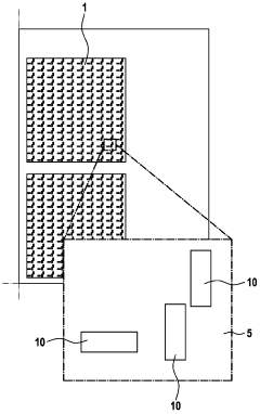
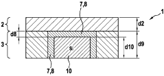
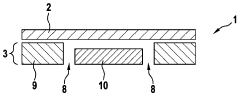
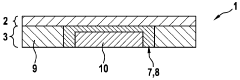
Warpage mitigation in printed circuit board assemblies
PatentActiveUS10178763B2
Innovation
- Incorporating heater traces within the PCB and interposer to maintain a uniform temperature profile, allowing controlled heating that reduces deformation and stress in solder joints, enabling the use of thinner PCBs without mechanical frames or clamps.


Industry Standards for PCB Warpage Control
The electronics industry has established comprehensive standards to address PCB warpage control, recognizing its critical impact on manufacturing yield and product reliability. The Institute for Printed Circuits (IPC) serves as the primary standardization body, with IPC-6012 defining acceptability criteria for rigid printed boards. This standard specifies maximum allowable warpage of 0.75% of the diagonal length for boards without surface mount components, and 0.5% for boards designated for surface mount assembly.
IPC-TM-650 Test Method 2.4.22 provides the standardized measurement procedure for determining bow and twist in printed boards. The method employs a precision measurement setup using dial indicators or laser-based systems to quantify deformation across the board surface. This measurement protocol ensures consistency across different manufacturing facilities and enables reliable quality control processes.
The JEDEC JESD22-B112 standard specifically addresses warpage measurement for surface mount applications, establishing temperature-dependent criteria that account for thermal cycling effects during reflow soldering. This standard recognizes that warpage behavior changes significantly with temperature, requiring dynamic measurement capabilities during actual assembly processes.
International standards such as IEC 61189-2 complement IPC specifications by providing additional guidance for high-density interconnect applications where warpage tolerances become increasingly stringent. These standards emphasize the relationship between material selection, stackup design, and warpage performance, establishing minimum requirements for copper balance and material property matching.
Recent updates to industry standards have incorporated advanced measurement techniques including shadow moiré interferometry and digital image correlation methods. These technologies enable real-time warpage monitoring during manufacturing processes, supporting implementation of closed-loop control systems that can adjust process parameters to maintain compliance with established limits.
The automotive electronics sector has developed additional stringent requirements through AEC-Q100 qualification standards, which mandate enhanced warpage control for safety-critical applications. These specifications often require warpage limits below 0.3% to ensure reliable solder joint formation and long-term mechanical integrity under harsh operating conditions.
IPC-TM-650 Test Method 2.4.22 provides the standardized measurement procedure for determining bow and twist in printed boards. The method employs a precision measurement setup using dial indicators or laser-based systems to quantify deformation across the board surface. This measurement protocol ensures consistency across different manufacturing facilities and enables reliable quality control processes.
The JEDEC JESD22-B112 standard specifically addresses warpage measurement for surface mount applications, establishing temperature-dependent criteria that account for thermal cycling effects during reflow soldering. This standard recognizes that warpage behavior changes significantly with temperature, requiring dynamic measurement capabilities during actual assembly processes.
International standards such as IEC 61189-2 complement IPC specifications by providing additional guidance for high-density interconnect applications where warpage tolerances become increasingly stringent. These standards emphasize the relationship between material selection, stackup design, and warpage performance, establishing minimum requirements for copper balance and material property matching.
Recent updates to industry standards have incorporated advanced measurement techniques including shadow moiré interferometry and digital image correlation methods. These technologies enable real-time warpage monitoring during manufacturing processes, supporting implementation of closed-loop control systems that can adjust process parameters to maintain compliance with established limits.
The automotive electronics sector has developed additional stringent requirements through AEC-Q100 qualification standards, which mandate enhanced warpage control for safety-critical applications. These specifications often require warpage limits below 0.3% to ensure reliable solder joint formation and long-term mechanical integrity under harsh operating conditions.
Thermal Management Impact on PCB Warpage Control
Thermal management plays a critical role in controlling PCB warpage, particularly in multilayer designs where differential thermal expansion creates significant mechanical stress. The relationship between temperature distribution and substrate deformation directly impacts wire sweep phenomena during assembly processes. Uneven heating patterns across the PCB surface generate localized thermal gradients that induce non-uniform expansion, leading to warpage that subsequently affects wire bond positioning and reliability.
The coefficient of thermal expansion (CTE) mismatch between different PCB materials becomes the primary driver of warpage-induced wire sweep issues. FR-4 substrates typically exhibit CTE values ranging from 14-17 ppm/°C in the X-Y plane, while copper traces demonstrate significantly lower expansion rates at approximately 17 ppm/°C. This differential expansion creates internal stress concentrations that manifest as substrate bowing, particularly pronounced in areas with high copper density or thick metallization layers.
Advanced thermal simulation techniques reveal that temperature variations exceeding 10°C across the PCB surface can generate warpage levels sufficient to cause measurable wire sweep displacement. The thermal time constant of different PCB regions varies substantially based on copper distribution, via density, and local thermal mass. Areas with dense via arrays or large copper pours exhibit slower thermal response times, creating transient thermal gradients during heating and cooling cycles.
Effective thermal management strategies for warpage control include implementing symmetrical copper distribution patterns, optimizing via placement for uniform heat dissipation, and incorporating thermal relief structures in high-stress regions. Controlled impedance routing techniques that balance copper density across layers help minimize differential thermal expansion effects. Additionally, strategic placement of thermal vias creates heat conduction pathways that reduce localized temperature peaks and associated warpage.
Modern PCB designs increasingly utilize embedded thermal management solutions, including metal core substrates and thermally conductive dielectric materials, to achieve more uniform temperature distribution. These approaches significantly reduce the thermal gradients responsible for warpage-induced wire sweep, enabling more predictable assembly outcomes in high-density interconnect applications.
The coefficient of thermal expansion (CTE) mismatch between different PCB materials becomes the primary driver of warpage-induced wire sweep issues. FR-4 substrates typically exhibit CTE values ranging from 14-17 ppm/°C in the X-Y plane, while copper traces demonstrate significantly lower expansion rates at approximately 17 ppm/°C. This differential expansion creates internal stress concentrations that manifest as substrate bowing, particularly pronounced in areas with high copper density or thick metallization layers.
Advanced thermal simulation techniques reveal that temperature variations exceeding 10°C across the PCB surface can generate warpage levels sufficient to cause measurable wire sweep displacement. The thermal time constant of different PCB regions varies substantially based on copper distribution, via density, and local thermal mass. Areas with dense via arrays or large copper pours exhibit slower thermal response times, creating transient thermal gradients during heating and cooling cycles.
Effective thermal management strategies for warpage control include implementing symmetrical copper distribution patterns, optimizing via placement for uniform heat dissipation, and incorporating thermal relief structures in high-stress regions. Controlled impedance routing techniques that balance copper density across layers help minimize differential thermal expansion effects. Additionally, strategic placement of thermal vias creates heat conduction pathways that reduce localized temperature peaks and associated warpage.
Modern PCB designs increasingly utilize embedded thermal management solutions, including metal core substrates and thermally conductive dielectric materials, to achieve more uniform temperature distribution. These approaches significantly reduce the thermal gradients responsible for warpage-induced wire sweep, enabling more predictable assembly outcomes in high-density interconnect applications.
Unlock deeper insights with PatSnap Eureka Quick Research — get a full tech report to explore trends and direct your research. Try now!
Generate Your Research Report Instantly with AI Agent
Supercharge your innovation with PatSnap Eureka AI Agent Platform!