

Understanding the Standards for Testing Optical Metasurface Materials
OCT 21, 20259 MIN READ
Generate Your Research Report Instantly with AI Agent
Patsnap Eureka helps you evaluate technical feasibility & market potential.
Optical Metasurface Testing Standards Background and Objectives
Optical metasurfaces represent a revolutionary advancement in the field of optics, offering unprecedented control over light manipulation at the nanoscale. The development of these engineered surfaces has evolved significantly over the past two decades, transitioning from theoretical concepts to practical applications across various industries. The historical trajectory began with fundamental research on metamaterials in the early 2000s, which subsequently led to the emergence of metasurfaces as a two-dimensional counterpart with enhanced functionality and fabrication feasibility.
The technological evolution of optical metasurfaces has been characterized by progressive improvements in design methodologies, fabrication techniques, and characterization methods. Early metasurfaces were primarily metallic structures with limited efficiency, while contemporary designs incorporate dielectric materials that significantly reduce losses and enhance performance. This transition represents a critical inflection point in the field's development, enabling applications previously deemed impractical.
Despite remarkable progress, standardized testing protocols for optical metasurface materials remain underdeveloped, creating significant challenges for industry adoption and commercialization. The absence of universally accepted measurement techniques and performance metrics impedes meaningful comparison between different metasurface designs and hinders quality control in manufacturing processes. This standardization gap represents a critical barrier to the technology's widespread implementation.
The primary objective of establishing comprehensive testing standards for optical metasurface materials is to facilitate reliable performance evaluation, ensure reproducibility, and accelerate technology transfer from research laboratories to commercial applications. These standards must address multiple aspects including optical performance metrics (efficiency, bandwidth, polarization control), material stability under various environmental conditions, and long-term reliability parameters.
Current trends indicate increasing interest in developing industry-wide testing protocols, with collaborative efforts emerging between academic institutions, national metrology institutes, and industrial stakeholders. Organizations such as ISO, ASTM International, and NIST have begun preliminary work on metasurface characterization standards, though these efforts remain in nascent stages.
The establishment of standardized testing methodologies would significantly impact the trajectory of metasurface technology development by providing clear benchmarks for performance evaluation, facilitating more effective communication between researchers and industry partners, and ultimately accelerating the commercialization timeline. As the field continues to mature, these standards will play an increasingly crucial role in ensuring the technology's successful integration into next-generation optical systems and devices.
Market Analysis for Optical Metasurface Applications
The optical metasurface market is experiencing significant growth, driven by increasing demand for miniaturized optical components across multiple industries. Current market valuations indicate the global optical metasurface market reached approximately 107 million USD in 2022, with projections suggesting a compound annual growth rate (CAGR) of 39.8% through 2030, potentially reaching 1.5 billion USD by the end of the forecast period.
Telecommunications represents the largest application segment, accounting for roughly 35% of market share. The integration of metasurfaces in 5G and upcoming 6G infrastructure for beam steering, signal focusing, and wavefront manipulation is creating substantial demand. Industry analysts predict this segment will maintain dominance through 2028 as telecommunications infrastructure continues to evolve globally.
Consumer electronics follows as the second-largest market segment at approximately 28% market share. Smartphone manufacturers are increasingly incorporating metasurface-based components for camera modules, sensors, and display technologies. Apple's recent patent filings suggest potential integration of metasurface lenses in future iPhone models, indicating growing commercial interest from major industry players.
The healthcare and medical devices sector represents the fastest-growing application segment with a projected CAGR of 44.2% through 2030. Applications include high-resolution medical imaging, biosensors, and targeted therapeutic devices. Several metasurface-based diagnostic tools have recently received regulatory approvals in Europe and are undergoing FDA review in the United States.
Aerospace and defense applications constitute approximately 15% of the current market, with significant investments in metasurface-based radar systems, stealth technology, and optical sensing. Government contracts, particularly in the United States, China, and European Union, are driving substantial R&D funding in this segment.
Regionally, North America leads with approximately 42% market share, followed by Asia-Pacific (31%) and Europe (21%). China is emerging as the fastest-growing regional market with substantial government investment in domestic metasurface research and manufacturing capabilities.
Key market challenges include high production costs, scalability issues, and lack of standardized testing protocols. The average cost of metasurface components remains 3-5 times higher than conventional optical elements, limiting mass-market adoption. However, recent manufacturing innovations by companies like Metalenz and Lumotive are gradually reducing production costs, potentially accelerating market penetration across various industries.
Current Testing Methodologies and Technical Barriers
The testing of optical metasurface materials currently employs a diverse range of methodologies, each with specific applications and limitations. Spectroscopic techniques, including reflectance and transmittance measurements, serve as fundamental approaches for characterizing the optical properties of metasurfaces. These methods provide essential data on wavelength-dependent behavior but often lack the spatial resolution necessary for detailed structural analysis.
Scanning electron microscopy (SEM) and atomic force microscopy (AFM) have emerged as critical tools for examining the nanoscale structural features of metasurfaces. SEM offers excellent resolution for surface topology visualization, while AFM provides precise three-dimensional profiling of surface structures. However, both techniques are limited to surface examination and cannot fully characterize internal material properties or dynamic optical responses.
Advanced characterization methods such as ellipsometry and near-field scanning optical microscopy (NSOM) enable more sophisticated analysis of optical properties. Ellipsometry measures polarization changes upon reflection or transmission, yielding information about material thickness and optical constants. NSOM achieves sub-wavelength spatial resolution by scanning a probe in close proximity to the sample surface, though this process is time-consuming and requires specialized equipment.
Despite these advancements, significant technical barriers persist in metasurface testing. The lack of standardized testing protocols represents a major challenge, as different laboratories employ varying methodologies, making cross-comparison of results difficult. This absence of standardization impedes consistent quality control and hampers industrial scalability of metasurface technologies.
The multiscale nature of metasurfaces presents another substantial challenge. These materials exhibit properties that span from nanometer to centimeter scales, requiring multiple complementary techniques for comprehensive characterization. Integrating data across these different scales remains problematic, often resulting in incomplete material understanding.
Environmental sensitivity poses additional testing difficulties, as metasurface properties can change significantly under different temperature, humidity, or pressure conditions. Most current testing occurs under controlled laboratory environments, potentially yielding results that poorly predict real-world performance.
Furthermore, dynamic testing capabilities remain underdeveloped. Many applications require metasurfaces to respond to changing conditions or external stimuli, yet most characterization techniques provide only static measurements. The development of methods for real-time, in-situ monitoring of metasurface performance represents a critical frontier in testing methodology advancement.
Standardized Testing Protocols and Procedures
01 Characterization methods for optical metasurfaces
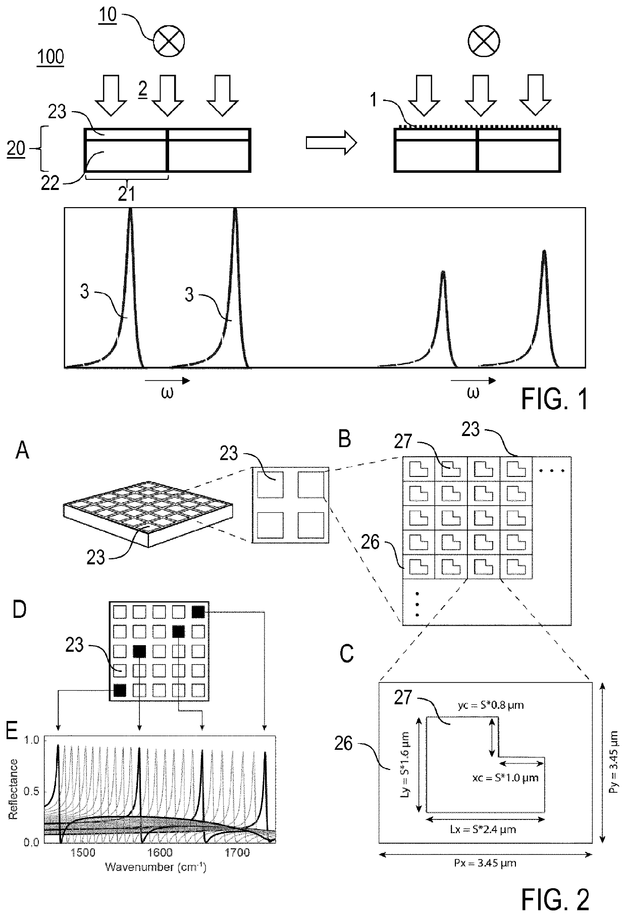
Various characterization techniques are employed to evaluate the performance of optical metasurfaces. These methods include spectroscopic analysis, wavefront measurement, and imaging techniques that assess the optical properties such as phase modulation, amplitude control, and polarization conversion efficiency. Advanced microscopy and interferometry are used to verify the structural integrity and optical functionality of metasurface components against design specifications.- Standardized testing methods for optical metasurfaces: Standardized testing methods are essential for evaluating the performance and quality of optical metasurfaces. These methods include specific procedures for measuring optical properties such as transmission, reflection, and phase modulation. The standards ensure consistency in testing across different laboratories and manufacturers, enabling reliable comparison of metasurface materials and designs. These testing protocols often include calibration procedures and reference samples to validate measurement accuracy.
- Characterization techniques for metasurface material properties: Various characterization techniques are employed to analyze the physical and optical properties of metasurface materials. These include scanning electron microscopy for structural analysis, spectroscopic ellipsometry for optical constant determination, and atomic force microscopy for surface topology examination. Advanced techniques such as near-field scanning optical microscopy allow for nanoscale resolution of optical responses. These characterization methods help in understanding the relationship between material composition, nanostructure geometry, and resulting optical performance.
- Quality control standards for metasurface fabrication: Quality control standards for metasurface fabrication ensure consistency and reliability in manufacturing processes. These standards define acceptable tolerances for feature dimensions, surface roughness, and material purity. They also specify inspection procedures to identify defects such as missing nanostructures, deformations, or contamination. Implementation of these quality control standards is crucial for scaling up production while maintaining the optical performance of metasurfaces across batches.
- Performance metrics and benchmarking for optical metasurfaces: Standardized performance metrics enable objective evaluation and benchmarking of optical metasurfaces. These metrics include efficiency, bandwidth, polarization sensitivity, and angular dependence of the optical response. Benchmarking protocols establish reference metasurface designs against which new developments can be compared. This standardization facilitates communication between researchers and industry, accelerates technology transfer, and helps in identifying the most promising metasurface designs for specific applications.
- Environmental durability testing for metasurface materials: Environmental durability testing assesses the stability and longevity of optical metasurfaces under various conditions. These tests evaluate resistance to temperature fluctuations, humidity, UV exposure, mechanical stress, and chemical exposure. Accelerated aging tests help predict long-term performance and identify potential failure modes. Standardized environmental testing is particularly important for metasurfaces intended for outdoor applications, aerospace, or other harsh environments where material degradation could compromise optical functionality.
02 Standardized testing protocols for metasurface quality control
Standardized testing protocols have been developed to ensure consistent quality control in metasurface manufacturing. These protocols include reference measurements, calibration procedures, and benchmark tests that allow for reproducible evaluation of metasurface performance across different laboratories and manufacturing facilities. The standards address parameters such as diffraction efficiency, spectral response, and durability under various environmental conditions.Expand Specific Solutions03 Environmental stability and reliability testing
Testing standards for optical metasurfaces include protocols for evaluating their environmental stability and long-term reliability. These tests assess the performance of metasurfaces under various conditions such as temperature fluctuations, humidity, mechanical stress, and prolonged exposure to light. Accelerated aging tests are employed to predict the lifetime and degradation patterns of metasurface materials in real-world applications.Expand Specific Solutions04 Fabrication tolerance and uniformity assessment
Standards for evaluating fabrication tolerance and uniformity are critical for optical metasurface materials. These standards define acceptable variations in feature dimensions, spacing, and alignment that still maintain the desired optical performance. Testing methods include high-resolution imaging, surface profiling, and statistical analysis of large-area metasurfaces to ensure manufacturing consistency and scalability for commercial applications.Expand Specific Solutions05 Integration and system-level performance testing
Testing standards for optical metasurfaces also address their integration into larger optical systems and devices. These standards evaluate how metasurfaces perform when combined with conventional optical components or integrated into specific applications such as sensors, displays, or communication systems. System-level tests measure parameters like signal-to-noise ratio, resolution, field of view, and overall efficiency to ensure that metasurfaces meet application-specific requirements.Expand Specific Solutions
Leading Research Institutions and Industry Players
The optical metasurface materials testing landscape is currently in a growth phase, with the market expanding rapidly due to increasing applications in telecommunications, consumer electronics, and automotive sectors. The global market size is projected to reach significant value as metasurfaces enable miniaturization and enhanced functionality in optical components. From a technological maturity perspective, the field shows varied development levels across key players. Research institutions like École Polytechnique Fédérale de Lausanne, Nanyang Technological University, and University of Michigan are advancing fundamental science, while companies including NIL Technology, Tokyo Electron, and KLA are developing commercial manufacturing and testing solutions. LG Electronics, Toyota, and BMW represent end-users integrating these technologies into consumer products, creating a complete ecosystem from research to application.
École Polytechnique Fédérale de Lausanne
Technical Solution: EPFL has pioneered academic research in metasurface testing methodologies, developing comprehensive characterization protocols that have influenced emerging industry standards. Their approach combines near-field scanning optical microscopy (NSOM) with far-field spectroscopic techniques to provide complete characterization across multiple length scales. EPFL researchers have established reference metasurfaces with precisely known optical properties that serve as calibration standards for testing equipment. Their methodology includes quantitative metrics for evaluating phase discontinuities, polarization conversion efficiency, and spectral response with nanometer-scale spatial resolution. EPFL has developed specialized testing procedures for dynamic metasurfaces, including protocols for measuring switching speeds, optical contrast ratios, and long-term stability under operational conditions. Their research has contributed significantly to ISO and IEC standardization efforts, particularly in establishing measurement traceability and uncertainty quantification for metasurface characterization.
Strengths: Cutting-edge research methodologies; comprehensive understanding of fundamental physics; established reference standards used internationally. Weaknesses: Technologies often at lower technology readiness levels; less focus on industrial throughput requirements; limited commercial product offerings compared to industry players.
ONTO INNOVATION INC
Technical Solution: Onto Innovation has developed advanced metrology systems specifically designed for optical metasurface characterization. Their technology combines white light interferometry with spectroscopic ellipsometry to provide comprehensive analysis of metasurface optical properties. Their Atlas® metrology platform incorporates multi-angle spectroscopic capabilities that can measure phase shifts, amplitude modulation, and polarization effects across the entire metasurface with nanometer-scale precision. The company has established testing protocols that align with emerging ISO standards for optical metasurface characterization, including measurements of diffraction efficiency, wavefront errors, and spectral response across varying angles of incidence. Their systems can detect defects as small as 10nm while maintaining high throughput for industrial applications.
Strengths: Industry-leading resolution in optical property measurements; integrated machine learning algorithms for defect classification; high throughput suitable for production environments. Weaknesses: Systems require significant capital investment; complex calibration procedures; limited to surface-level characterization without subsurface analysis capabilities.
Critical Metasurface Performance Metrics and Evaluation Methods
Method for preparing optical metasurfaces
PatentInactiveUS20210216009A1
Innovation
- The use of nano-imprinting technology with an imprinting template featuring meta-atom patterns, allowing for low-cost, large-scale fabrication of optical metasurfaces in a short time, replacing the need for electron beam lithography.

Method and spectrometer apparatus for investigating an infrared absorption of a sample
PatentActiveUS20210239605A1
Innovation
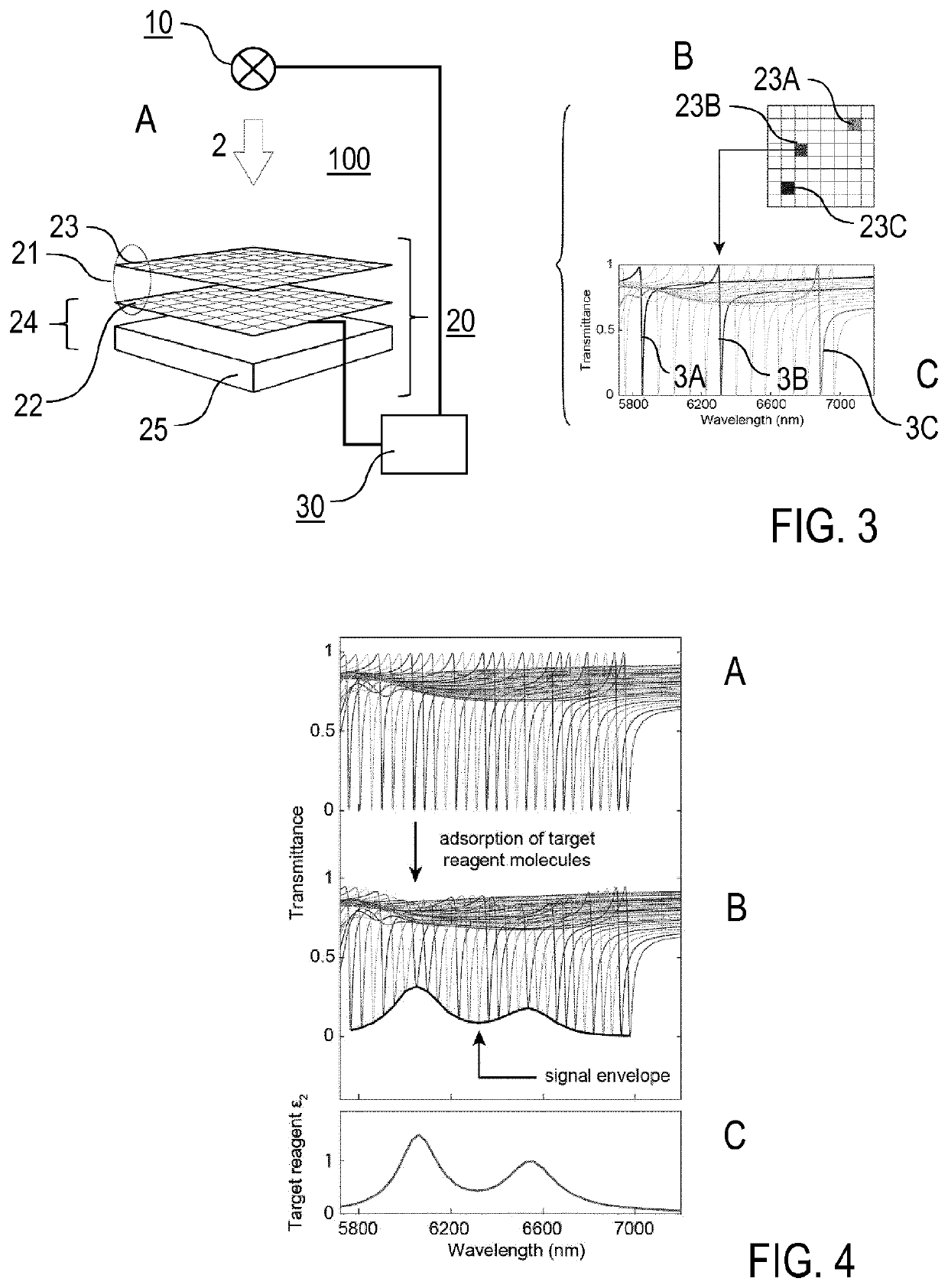
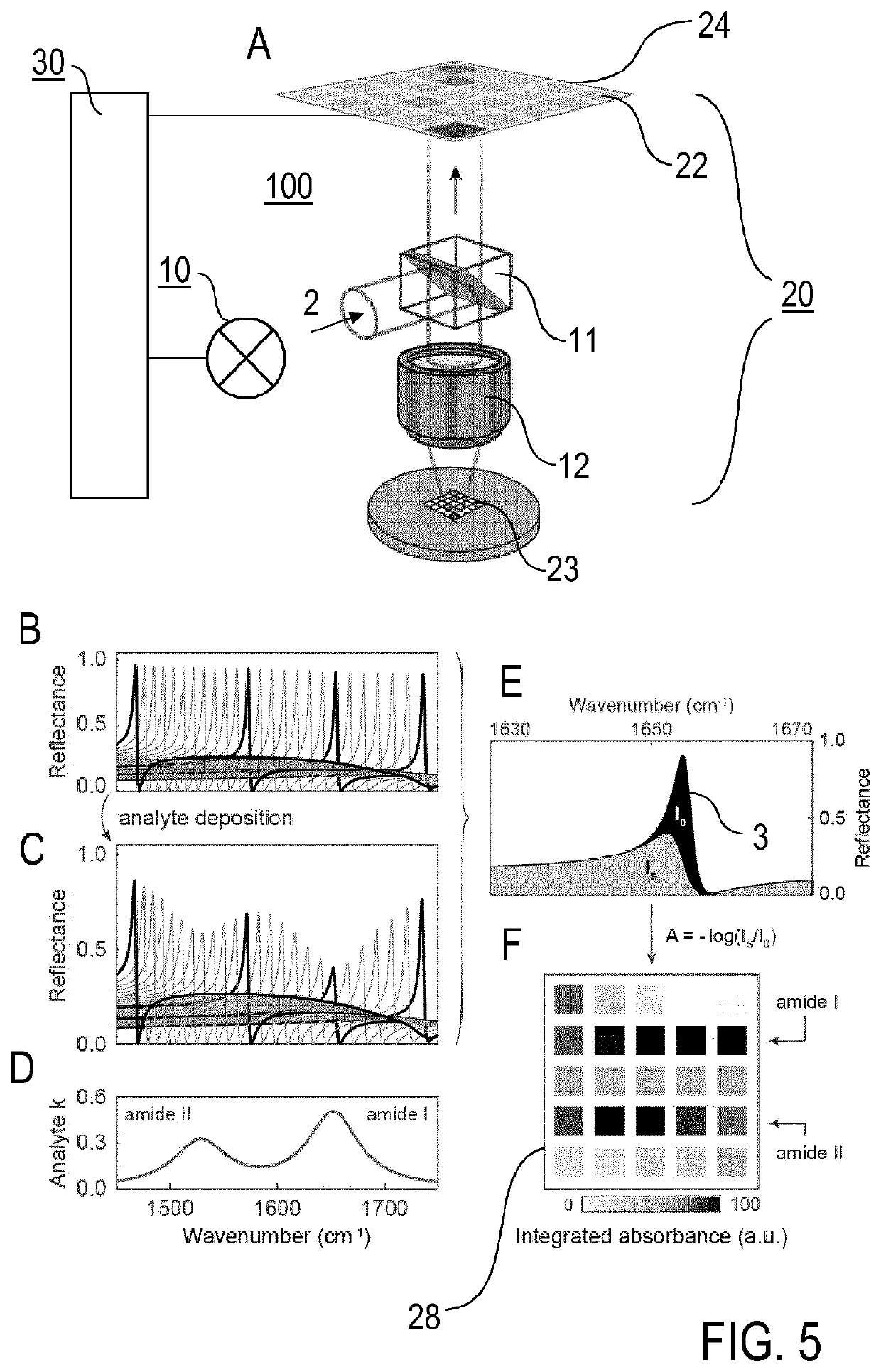
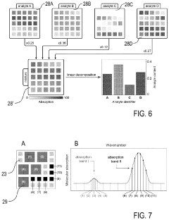
- A method and spectrometer apparatus utilizing a pixelated metasurface with dielectric metamaterial resonator sections, each with a specific spectral resonance line within the infrared range, enabling near-field coupling for enhanced sensitivity and allowing detection of molecular fingerprints without the need for light dispersive elements or moving parts, using broadband light sources and micro-bolometer cells for high spatial resolution.
International Standardization Efforts and Harmonization
The global landscape of metasurface material testing standards remains fragmented, with different regions developing their own protocols and methodologies. Recognizing this challenge, several international organizations have initiated efforts to harmonize these standards across borders. The International Organization for Standardization (ISO) has established technical committees specifically focused on nanomaterials and optical metasurfaces, working to develop unified testing frameworks that can be adopted worldwide.
In parallel, the International Electrotechnical Commission (IEC) has been collaborating with industry stakeholders to address the electrical and optical characterization aspects of metasurface materials. Their TC 113 committee on nanotechnology standardization has published several standards relevant to metasurface characterization, creating a foundation for international consensus.
The IEEE Standards Association has also contributed significantly through its P1928 working group, which focuses on standardizing measurement techniques for electromagnetic properties of materials, including metasurfaces. These efforts aim to establish common terminology, measurement protocols, and reporting formats that facilitate global research collaboration and industrial application.
Regional standardization bodies such as ASTM International in North America, CEN in Europe, and SAC in China have been working to align their metasurface testing standards with international frameworks while addressing specific regional needs. This multi-level approach ensures both global compatibility and local relevance.
Cross-border research initiatives like the International Metasurface Testing Consortium (IMTC) have emerged to bridge gaps between academic research and industrial implementation. These consortia bring together experts from different countries to conduct round-robin testing, validate methodologies across laboratories, and establish reproducible protocols for optical metasurface characterization.
Harmonization efforts face several challenges, including varying measurement capabilities across regions, different regulatory frameworks, and competing industrial interests. To address these challenges, international standards organizations are implementing phased approaches that begin with standardizing terminology and basic measurement techniques before progressing to more complex characterization methods.
The development of reference materials and calibration standards represents another critical aspect of international harmonization. Organizations like NIST in the US, PTB in Germany, and NIM in China are collaborating to develop certified reference metasurfaces that can serve as benchmarks for testing laboratories worldwide, ensuring measurement consistency regardless of geographic location.
Material Fabrication Quality Control Considerations
Quality control in the fabrication of optical metasurface materials represents a critical aspect of ensuring consistent performance and reliability. The manufacturing processes for metasurfaces typically involve nanofabrication techniques such as electron beam lithography, focused ion beam milling, or nanoimprint lithography, each requiring stringent quality control protocols. These protocols must address dimensional accuracy, structural uniformity, and material purity to achieve the desired optical properties.
Surface roughness measurements serve as a primary quality control metric, as even nanometer-scale imperfections can significantly impact the optical performance of metasurfaces. Advanced metrology techniques including atomic force microscopy (AFM) and scanning electron microscopy (SEM) are employed to quantify surface roughness parameters such as Ra (arithmetic average) and Rq (root mean square) values, with industry standards typically requiring Ra values below 5 nm for high-performance optical applications.
Dimensional tolerance verification constitutes another essential quality control consideration. The periodic structures in metasurfaces must maintain precise spacing and geometry to achieve the designed electromagnetic response. Fabrication facilities typically implement in-line optical diffraction measurements to verify pattern fidelity, with acceptable dimensional variations generally limited to ±2% of the design specifications to prevent performance degradation.
Material composition analysis through techniques such as X-ray photoelectron spectroscopy (XPS) and energy-dispersive X-ray spectroscopy (EDX) ensures the chemical purity and stoichiometry of deposited materials. Contamination levels must typically remain below 0.1% for critical optical applications, as impurities can introduce unwanted absorption or scattering effects that compromise metasurface functionality.
Process repeatability represents a significant challenge in metasurface fabrication quality control. Statistical process control (SPC) methodologies are increasingly being adopted to monitor key process parameters and identify drift before it impacts product quality. This approach typically involves establishing control charts for critical dimensions, optical properties, and defect rates, with action limits set at ±3σ from target values.
Defect inspection systems utilizing automated optical or electron microscopy enable comprehensive surface analysis to identify and classify defects such as pinholes, particles, or pattern distortions. Modern inspection systems can detect defects as small as 10 nm, with acceptance criteria typically specifying maximum allowable defect densities (often <0.1 defects/cm²) and size distributions based on their impact on optical performance.
Environmental control during fabrication constitutes a final critical consideration, with temperature stability typically maintained within ±0.5°C and humidity levels controlled to ±2% RH to prevent dimensional instability or contamination. Cleanroom classifications for metasurface production generally require ISO Class 5 (Class 100) or better environments to minimize particulate contamination during critical process steps.
Unlock deeper insights with Patsnap Eureka Quick Research — get a full tech report to explore trends and direct your research. Try now!
Generate Your Research Report Instantly with AI Agent
Supercharge your innovation with Patsnap Eureka AI Agent Platform!