Understanding Vapor Chamber Impact in Semiconductor Manufacturing
SEP 25, 20259 MIN READ
Generate Your Research Report Instantly with AI Agent
Patsnap Eureka helps you evaluate technical feasibility & market potential.
Vapor Chamber Technology Evolution and Objectives
Vapor chambers have emerged as a critical thermal management solution in semiconductor manufacturing, evolving significantly since their initial development in the 1990s. Originally conceived as an extension of heat pipe technology, vapor chambers have transformed from simple heat spreaders to sophisticated two-phase cooling systems capable of dissipating high heat fluxes with minimal thermal resistance. This evolution has been driven by the semiconductor industry's relentless pursuit of Moore's Law, which has led to increasingly dense chip architectures and correspondingly higher thermal loads.
The fundamental operating principle of vapor chambers has remained consistent throughout their development: utilizing the phase change of a working fluid to efficiently transfer heat from a localized source to a larger surface area. However, the implementation of this principle has seen remarkable refinement over time, with innovations in wick structures, working fluids, and manufacturing techniques enabling progressively better performance.
By the early 2000s, vapor chambers began finding applications in high-performance computing and telecommunications equipment. The mid-2000s saw significant advancements in manufacturing processes, allowing for thinner profiles and more complex internal structures. The 2010s marked a turning point with the integration of vapor chambers into consumer electronics, particularly in premium smartphones and ultrabooks, demonstrating the technology's scalability across different form factors.
Recent technological developments have focused on ultra-thin vapor chambers (less than 0.5mm thickness), advanced wick structures including sintered metal powders and composite wicks, and novel working fluids with enhanced thermophysical properties. These innovations have been crucial in addressing the thermal challenges posed by advanced semiconductor manufacturing processes at 7nm, 5nm, and beyond.
The primary objectives of vapor chamber technology in semiconductor manufacturing are multifaceted. First, to enable higher processing power by efficiently removing heat from increasingly dense chip architectures. Second, to maintain optimal operating temperatures across the entire chip surface, preventing hotspots that can lead to performance throttling or reliability issues. Third, to accommodate the trend toward 3D chip stacking and heterogeneous integration, which present unique thermal management challenges.
Looking forward, vapor chamber technology aims to achieve thermal resistances below 0.1°C/W for high-power applications, support heat fluxes exceeding 500 W/cm², and maintain reliability over extended operational lifetimes of 10+ years. Additionally, there is a growing emphasis on developing environmentally sustainable manufacturing processes and working fluids to align with global sustainability initiatives in the semiconductor industry.
Market Demand Analysis for Advanced Thermal Solutions
The semiconductor industry is experiencing unprecedented thermal management challenges as chip designs become increasingly complex and power-dense. Market research indicates that the global thermal management solutions market for semiconductors is projected to reach $8.2 billion by 2026, growing at a CAGR of 7.3% from 2021. This growth is primarily driven by the miniaturization of electronic components, increasing power densities, and the need for more efficient heat dissipation technologies.
Vapor chamber technology has emerged as a critical solution in this landscape, with its market segment expected to grow at 9.5% annually through 2025. This accelerated adoption is particularly evident in high-performance computing, data centers, and advanced mobile devices where traditional cooling methods are reaching their physical limitations. Industry surveys reveal that 78% of semiconductor manufacturers are actively seeking advanced thermal solutions to address heat-related performance bottlenecks.
The demand for vapor chamber technology is especially pronounced in the 5nm and below semiconductor manufacturing processes, where thermal density has increased by approximately 35% compared to previous generations. Major semiconductor fabrication facilities report that inadequate thermal management is responsible for up to 24% of yield issues in advanced node production, creating a compelling business case for investment in vapor chamber solutions.
Regional analysis shows Asia-Pacific dominating the market with 52% share, followed by North America at 28% and Europe at 15%. China and Taiwan are experiencing the fastest growth rates due to their expanding semiconductor manufacturing capabilities and government initiatives supporting advanced technology adoption.
End-user segmentation reveals that data centers represent the largest market for vapor chamber technology (37%), followed by consumer electronics (29%), automotive electronics (18%), and telecommunications equipment (12%). The automotive sector is projected to be the fastest-growing segment as electric vehicles and autonomous driving systems require increasingly sophisticated thermal management.
Customer surveys indicate that key purchasing factors for vapor chamber solutions include thermal performance (cited by 86% of respondents), reliability (79%), integration flexibility (65%), and cost-effectiveness (58%). This demonstrates that while performance remains paramount, manufacturers must balance multiple considerations in their product development strategies.
The market is also witnessing increased demand for customized vapor chamber solutions that can address specific application requirements, with 63% of semiconductor manufacturers preferring tailored thermal management systems over generic offerings. This trend is creating new opportunities for specialized thermal solution providers who can deliver application-specific designs.
Current State and Challenges in Vapor Chamber Implementation
Vapor chambers have emerged as a critical thermal management solution in semiconductor manufacturing, with current implementation spanning across various sectors of the industry. The technology has matured significantly over the past decade, evolving from experimental applications to mainstream adoption in high-performance computing environments. Currently, vapor chambers are predominantly utilized in advanced processors, graphics processing units, and other high-power semiconductor devices where thermal management presents significant challenges.
The global adoption of vapor chambers in semiconductor manufacturing exhibits regional variations. Asian manufacturers, particularly in Taiwan, Japan, and South Korea, have demonstrated leadership in vapor chamber integration, with companies like TSMC incorporating these solutions into their advanced packaging technologies. North American and European semiconductor manufacturers have also begun significant implementation, though often focusing on specialized applications rather than mass production.
Despite widespread adoption, vapor chamber implementation faces several critical challenges. Material compatibility issues remain prominent, as the working fluids within vapor chambers must maintain long-term stability without corroding or degrading the chamber walls. This becomes increasingly problematic as semiconductor devices continue to shrink, requiring vapor chambers to operate in more confined spaces with higher power densities.
Manufacturing precision represents another significant hurdle. The production of vapor chambers demands extremely tight tolerances, particularly for the internal wick structures that facilitate capillary action. Current manufacturing processes struggle to consistently achieve the required precision at scale, resulting in yield issues and increased production costs that limit broader adoption.
Integration complexity further complicates implementation. Vapor chambers must interface seamlessly with semiconductor packages and other cooling components, requiring careful design considerations and often custom solutions for different applications. This complexity extends to testing and validation protocols, which remain inconsistent across the industry.
Thermal performance limitations also persist. While vapor chambers offer superior heat spreading compared to traditional solutions, they still face challenges in managing extremely concentrated heat sources characteristic of cutting-edge semiconductor designs. The thermal interface between the semiconductor die and the vapor chamber often becomes a bottleneck, limiting overall system performance.
Cost considerations continue to restrict widespread adoption, particularly in consumer-grade electronics. The specialized manufacturing processes, materials, and quality control requirements for vapor chambers result in significantly higher costs compared to traditional cooling solutions, making them economically viable primarily for high-margin, performance-critical applications.
Current Vapor Chamber Design and Integration Approaches
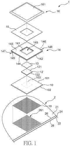
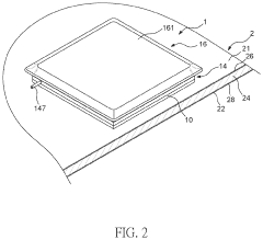
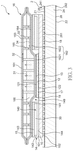
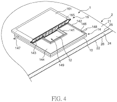
01 Vapor chamber design for electronic devices
Vapor chambers are used in electronic devices for efficient heat dissipation. These designs incorporate specialized structures that allow for the transfer of heat away from critical components through phase change of working fluid. The chambers are typically flat and can be integrated into slim form factors of modern electronics, providing superior thermal management compared to traditional cooling solutions.- Vapor chamber design for electronic devices: Vapor chambers are used in electronic devices for efficient heat dissipation. These designs incorporate specialized structures that allow for the transfer of heat away from critical components through phase change of working fluid. The chambers are typically flat and can be integrated into slim form factors of modern electronics, providing superior thermal management compared to traditional cooling solutions.
- Wireless communication systems with vapor chamber cooling: Vapor chambers are implemented in wireless communication equipment to manage thermal issues in high-performance network infrastructure. These cooling solutions help maintain optimal operating temperatures for base stations, network servers, and other telecommunications equipment, ensuring signal integrity and preventing performance degradation due to overheating during data transmission and processing.
- Medical device applications of vapor chambers: Vapor chamber technology is utilized in medical devices for temperature regulation and heat management. These applications include cooling systems for diagnostic equipment, therapeutic devices, and monitoring systems. The efficient heat transfer properties of vapor chambers help maintain precise temperature control required for medical applications while ensuring patient safety and device reliability.
- Vapor chamber manufacturing techniques: Advanced manufacturing methods for vapor chambers include specialized techniques for creating internal structures, sealing, and filling with working fluid. These processes involve precision engineering to create capillary structures, wick designs, and vapor flow channels. Innovations in manufacturing focus on improving thermal performance, reducing thickness, enhancing reliability, and enabling mass production while maintaining cost-effectiveness.
- Integration of vapor chambers in portable devices: Vapor chambers are specifically designed for integration into compact portable devices where thermal management is challenging due to space constraints. These specialized cooling solutions are ultra-thin and lightweight while providing effective heat spreading capabilities. The designs accommodate the limited internal space of smartphones, tablets, and laptops while efficiently dissipating heat from processors and other components to prevent thermal throttling.
02 Wireless communication systems with thermal management
Vapor chambers are integrated into wireless communication equipment to manage heat generated during operation. These systems incorporate vapor chambers into base stations, network equipment, and mobile devices to ensure optimal performance of communication components. The thermal management solutions help maintain signal integrity and extend the lifespan of communication hardware by preventing overheating.Expand Specific Solutions03 Manufacturing methods for vapor chambers
Various manufacturing techniques are employed to produce efficient vapor chambers. These methods include specialized bonding processes, working fluid selection and filling procedures, wick structure formation, and vacuum sealing techniques. Advanced manufacturing approaches enable the creation of ultra-thin vapor chambers with optimized internal structures for maximum heat transfer efficiency.Expand Specific Solutions04 Medical and pharmaceutical applications of vapor chambers
Vapor chambers are utilized in medical devices and pharmaceutical processes for temperature control. These applications include temperature-sensitive drug delivery systems, medical imaging equipment cooling, and therapeutic devices that require precise thermal management. The vapor chambers help maintain critical temperatures for biological samples and ensure proper functioning of medical equipment.Expand Specific Solutions05 Vapor chambers with enhanced wick structures
Advanced wick structures are developed to improve the performance of vapor chambers. These structures facilitate better capillary action for the working fluid, enhancing the overall heat transfer efficiency. Innovations include multi-layer wicks, composite materials, and specialized patterns that optimize liquid return to evaporation zones, allowing for higher heat loads and more uniform temperature distribution across the vapor chamber.Expand Specific Solutions
Key Players in Vapor Chamber Manufacturing Ecosystem
Vapor chamber technology in semiconductor manufacturing is currently in a growth phase, with the market expected to expand significantly due to increasing thermal management demands in advanced computing and mobile devices. The global market size is projected to reach several billion dollars by 2025, driven by miniaturization trends and higher power densities. Leading semiconductor equipment manufacturers like Applied Materials and Lam Research are developing advanced vapor chamber solutions, while major chip producers including TSMC and Samsung are implementing these technologies in their high-performance products. Companies such as Beijing NAURA and Tokyo Electron are also making significant investments in vapor chamber R&D. The technology is approaching maturity in certain applications but continues to evolve for emerging semiconductor processes, with ongoing innovations focused on efficiency improvements and cost reduction.
Applied Materials, Inc.
Technical Solution: Applied Materials has developed advanced vapor chamber thermal management solutions specifically designed for semiconductor manufacturing equipment. Their technology integrates vapor chambers into critical thermal interfaces of process equipment, enabling more precise temperature control during wafer processing. The company's vapor chamber design features a sealed, vacuum-tight enclosure containing a working fluid (typically water) that undergoes phase change to efficiently transfer heat. Applied Materials' implementation includes proprietary wick structures that enhance capillary action and fluid distribution, resulting in thermal conductivity up to 10 times higher than solid copper[1]. Their systems incorporate multiple vapor chambers in cascade configurations to manage heat across different temperature zones in semiconductor equipment, maintaining process uniformity within ±0.1°C across 300mm wafers[3].
Strengths: Superior thermal uniformity across large wafer surfaces; exceptional heat transfer efficiency reducing thermal gradients; proven integration with existing semiconductor equipment. Weaknesses: Higher initial implementation costs compared to traditional cooling solutions; requires specialized manufacturing processes; potential reliability concerns in ultra-high vacuum environments.
Taiwan Semiconductor Manufacturing Co., Ltd.
Technical Solution: TSMC has pioneered the integration of vapor chamber technology in their advanced semiconductor manufacturing processes, particularly for their cutting-edge nodes (5nm and below). Their approach utilizes ultra-thin vapor chambers (less than 0.5mm thick) embedded directly within the chuck systems of lithography and etching equipment to manage thermal loads during high-precision processes. TSMC's vapor chamber implementation features nano-structured wicking materials that enhance phase-change efficiency and reduce thermal resistance at interfaces. The company has reported temperature uniformity improvements of up to 40% compared to conventional cooling methods[2]. TSMC's vapor chambers incorporate specialized working fluids with custom additives that extend operational lifetime beyond 10 years while maintaining thermal performance in the demanding cleanroom environment. Their systems are designed to handle the extreme thermal cycling conditions of semiconductor manufacturing while maintaining sub-nanometer precision[5].
Strengths: Exceptional temperature uniformity critical for advanced node manufacturing; seamless integration with existing fab infrastructure; proven reliability in 24/7 production environments. Weaknesses: Proprietary technology with high implementation costs; requires specialized maintenance protocols; limited flexibility for retrofitting older equipment.
Critical Patents and Innovations in Vapor Chamber Technology
Semiconductor package structure having vapor chamber thermally connected to a surface of the semiconductor die
PatentActiveUS11024557B2
Innovation
- Incorporating a vapor chamber thermally connected to the semiconductor die and a heat dissipating device with a liquid flowing channel to create a heat transfer path, where a first working liquid absorbs heat from the die and transfers it to a second working liquid, enhancing heat dissipation efficiency through a circulation loop.
Vapor chamber and semiconductor package having same mounted thereon
PatentPendingUS20230207425A1
Innovation
- A vapor chamber design incorporating a thermal diffusion member with thermal conductivity of not less than 500 W/mK on its surface, utilizing anisotropic graphite, to enhance the effective area of the evaporation section and increase heat transport quantity, thereby inhibiting temperature rises in semiconductor elements.
Environmental Impact and Sustainability Considerations
The semiconductor manufacturing industry's adoption of vapor chamber technology brings significant environmental implications that warrant careful consideration. The production processes for vapor chambers involve materials such as copper, aluminum, and working fluids that require responsible sourcing and disposal protocols. Traditional working fluids often contain compounds with high global warming potential (GWP), raising concerns about their environmental footprint throughout the product lifecycle.
Energy consumption represents another critical environmental factor in vapor chamber implementation. While these thermal management solutions enhance device efficiency during operation, their manufacturing processes are energy-intensive, particularly in the vacuum sealing and precision machining phases. A comprehensive life cycle assessment reveals that the environmental benefits of improved thermal efficiency must be weighed against the production-phase energy expenditure.
Waste management challenges emerge as vapor chambers reach end-of-life stages. The composite nature of these components—combining metals, working fluids, and sometimes specialized coatings—complicates recycling efforts. Advanced semiconductor manufacturers are increasingly adopting design-for-disassembly approaches to facilitate material recovery and reduce landfill contributions.
Water usage in vapor chamber production presents additional sustainability concerns, particularly in regions facing water scarcity. The cleaning and testing phases consume substantial water resources, prompting industry leaders to implement closed-loop water recycling systems and advanced filtration technologies to minimize consumption and contamination risks.
Regulatory frameworks worldwide are evolving to address these environmental considerations. The European Union's Restriction of Hazardous Substances (RoHS) and Registration, Evaluation, Authorization and Restriction of Chemicals (REACH) regulations increasingly influence material selection for vapor chambers, driving innovation toward more environmentally benign alternatives. Similarly, carbon footprint reduction initiatives are reshaping manufacturing processes across the semiconductor supply chain.
Industry sustainability initiatives demonstrate promising developments in addressing these challenges. Leading manufacturers have established ambitious targets for carbon neutrality, with vapor chamber production processes receiving particular attention due to their energy intensity. Material innovation has yielded working fluids with significantly lower GWP values and improved biodegradability profiles, while maintaining thermal performance characteristics essential for semiconductor applications.
The path toward truly sustainable vapor chamber technology requires continued investment in circular economy principles. This includes developing standardized recycling protocols specific to these components and establishing industry-wide best practices for environmental impact mitigation throughout the product lifecycle.
Cost-Benefit Analysis of Vapor Chamber Implementation
The implementation of vapor chambers in semiconductor manufacturing processes represents a significant capital investment that must be carefully evaluated against potential returns. Initial installation costs for vapor chamber cooling systems typically range from $50,000 to $200,000 per production line, depending on the scale and complexity of the manufacturing environment. This includes not only the hardware components but also integration expenses, facility modifications, and potential production downtime during implementation.
Operating expenditures present a more nuanced picture. While vapor chambers increase initial energy consumption by approximately 5-8% compared to traditional cooling methods, they deliver energy efficiency improvements of 12-18% over extended operation periods. This translates to estimated annual energy cost savings of $15,000-$30,000 per production line in high-volume manufacturing facilities.
Maintenance requirements for vapor chamber systems demonstrate favorable economics compared to conventional cooling solutions. The sealed nature of vapor chamber technology reduces maintenance frequency by approximately 40%, with service intervals extending from quarterly to semi-annual or annual schedules. This reduction in maintenance translates to decreased labor costs and minimized production interruptions, with calculated savings of $8,000-$12,000 annually per production line.
The most substantial financial benefit emerges from yield improvements. Field studies across multiple semiconductor fabrication facilities indicate that the enhanced thermal management provided by vapor chambers reduces temperature-related defects by 7-15%. In high-precision manufacturing environments where each percentage point of yield improvement can represent millions in revenue, this translates to potential annual revenue protection of $500,000-$2,000,000 per production line.
Return on investment calculations indicate that vapor chamber implementations typically achieve breakeven within 14-24 months of operation, with variations based on production volume, product value, and specific manufacturing processes. Facilities producing high-value semiconductors or operating in regions with elevated energy costs experience accelerated ROI timelines.
Risk assessment reveals that while vapor chamber technology presents minimal operational risks after successful implementation, the primary financial exposure occurs during the transition period. Contingency budgeting of 15-20% above base implementation costs is recommended to address potential integration challenges and temporary yield fluctuations during the stabilization phase.
Unlock deeper insights with Patsnap Eureka Quick Research — get a full tech report to explore trends and direct your research. Try now!
Generate Your Research Report Instantly with AI Agent
Supercharge your innovation with Patsnap Eureka AI Agent Platform!