
Capacitive Sensor Demodulation for Interference Avoidance
Find Innovative SolutionsGenerate Solutions
Solution Overview
Problem
Capacitive sensing devices in touch screens and touchpads face interference issues due to noise and electromagnetic signals, which affect the accuracy of input detection and user interaction.
Innovation Solution
The integration of capacitive sensor devices with display devices shares components to utilize varying demodulation frequencies and shifting carrier frequencies, allowing for interference avoidance by timing transmitter signal transitions during non-display update times and using different demodulation schemes to filter out noise.
Engineering Contradictions & Design Principles
Engineering Contradiction Analysis
1Device complexity
If capacitive sensing devices share components with display devices, then device complexity is reduced and integration is improved, but interference from electromagnetic signals and noise increases
Solution Approach 1:
The patent implements dynamic frequency selection where the demodulation frequency is varied based on detected interference conditions. The system monitors for interference patterns and adjusts the demodulation frequency accordingly, transforming a static sensing system into a dynamic one that adapts to changing electromagnetic environments, thereby resolving the contradiction between integration and interference.
Solution Approach 2:
The patent changes the demodulation frequency parameter in response to detected interference. By monitoring the electromagnetic environment and adjusting the demodulation frequency parameter, the system maintains accurate capacitive sensing despite shared components with display devices, thus resolving the contradiction between component integration and electromagnetic interference.
2Measurement precision
If demodulation frequency is varied to avoid interference, then signal-to-noise ratio is improved, but processing complexity increases
Solution Approach 1:
The patent performs preliminary interference detection before demodulation by monitoring for specific interference patterns and characteristics. This preliminary action allows the system to pre-select an appropriate demodulation frequency that avoids detected interference, improving signal-to-noise ratio without requiring complex real-time processing during the actual sensing operation.
Solution Approach 2:
The patent implements a feedback mechanism where the system monitors for interference patterns, detects their presence and characteristics, and uses this feedback to adjust the demodulation frequency. This closed-loop feedback system improves measurement precision by adapting to interference conditions while keeping processing complexity manageable through structured feedback handling.
3Object-affected harmful factors
If transmitter signal transitions are timed during non-display update times, then interference is minimized, but sensing speed is reduced
Solution Approach 1:
The patent utilizes periodic non-display update times (such as vertical blanking intervals in LCD refresh cycles) to perform capacitive sensing operations. By scheduling sensing transmissions during these periodic intervals when the display is not updating, the system minimizes electromagnetic interference while maintaining acceptable sensing speeds through efficient use of available time windows.
Solution Approach 2:
The patent performs sensing operations during only portions of the available time (specifically during non-display update intervals), accepting that not all time is utilized for sensing. This partial action approach minimizes interference by avoiding display update times, while the system compensates for reduced sensing speed through efficient processing during the available windows and by updating sensing rates as needed.
Applied Scientific Principles
This section explains which scientific principles are used to turn an abstract innovation direction into a practical engineering solution.
Function Achieved in This Case
This approach enhances the signal-to-noise ratio and improves the accuracy of input detection by minimizing interference, enabling reliable user input recognition without compromising display performance.
Implementation Method 1
a sensing element that produces an electrical signal in response to a change in capacitance caused by an input object (such as a finger or stylus) in a sensing region
Implementation Method 2
a transmitter electrode that transmits a transmitter signal
Implementation Method 3
a receiver electrode that receives a resulting signal that corresponds to the transmitted transmitter signal
Implementation Method 4
demodulating the received resulting signal
Data Source
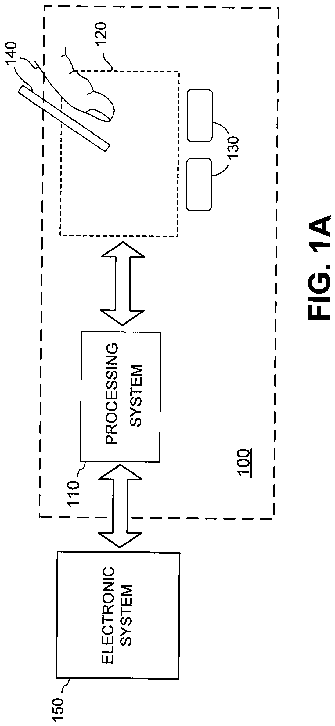 Figure 1A
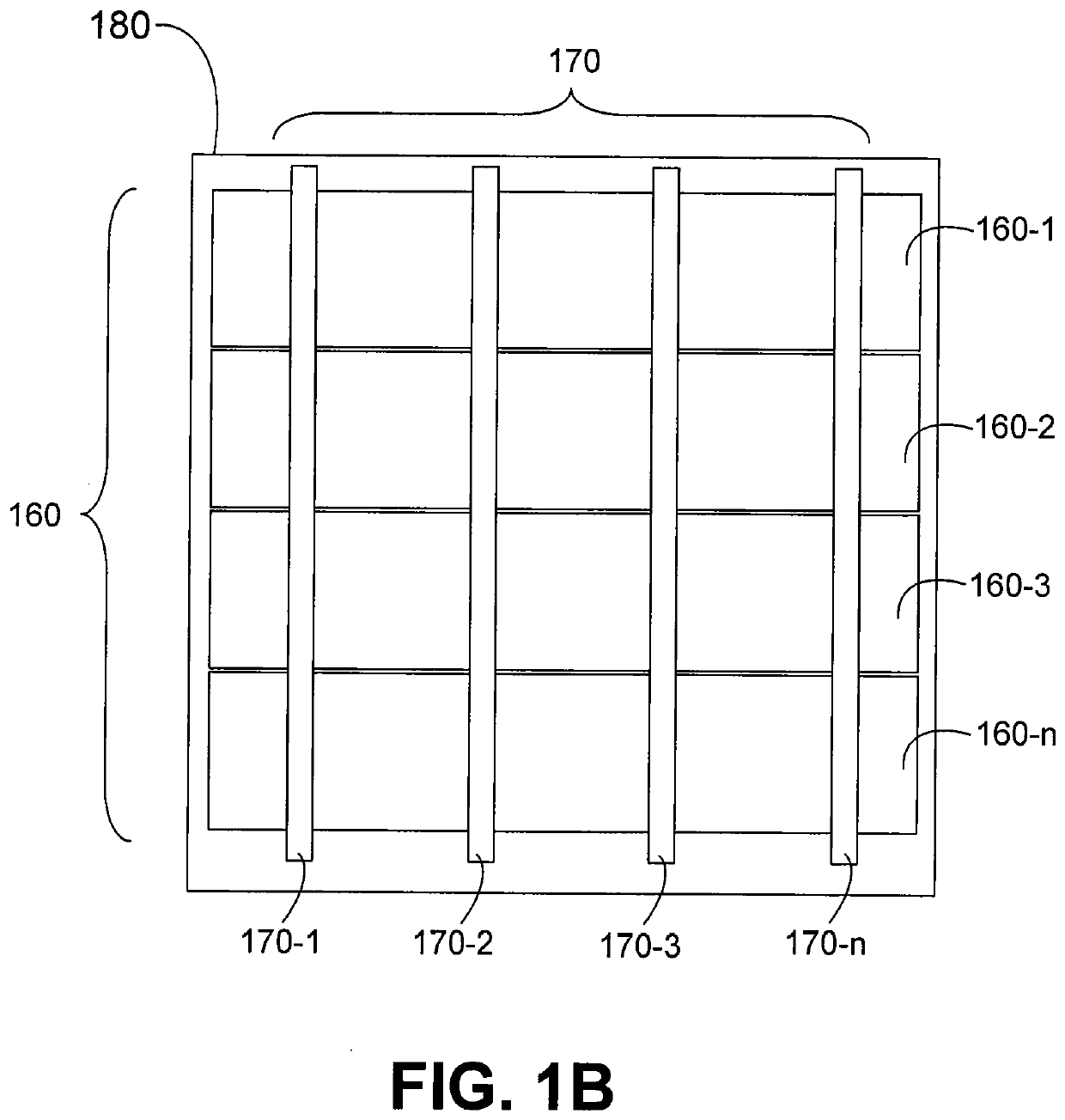 Figure 1B
 Figure 1C~1D
AI summary
In a method of interference avoidance for a capacitive sensor device, a transmitter signal is transmitted with a transmitter electrode of the capacitive sensor device. A resulting signal is received with a receiver electrode of the capacitive sensor device. The resulting signal corresponds to the transmitter signal. A first demodulated output is acquired by demodulating the resulting signal in a first way. A second demodulated output is acquired by demodulating the resulting signal in a second way, where the second way and the first way differ. A shift is made from using the first demodulated output for determining positional information to using the second demodulated output for determining positional information. The shift is based at least in part upon an amount of interference.