
Semiconductor Memory Power Supply Status Determination Circuit
Find Innovative SolutionsGenerate Solutions
Solution Overview
Problem
Conventional non-volatile semiconductor memory devices require a dedicated terminal for outputting a ready_to_read signal, increasing the number of terminals and potentially leading to erroneous data reading due to incomplete power supply circuit operations.
Innovation Solution
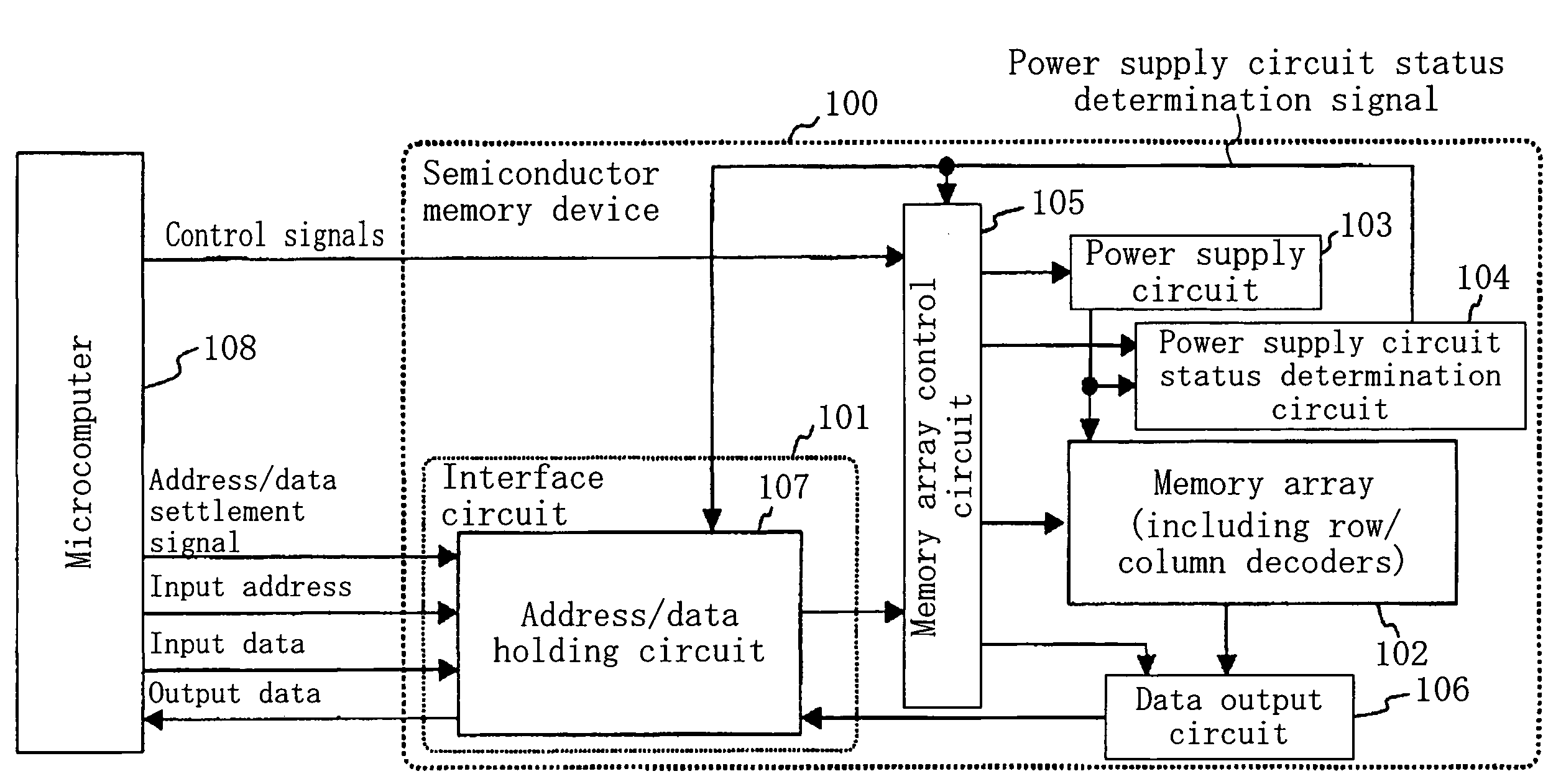
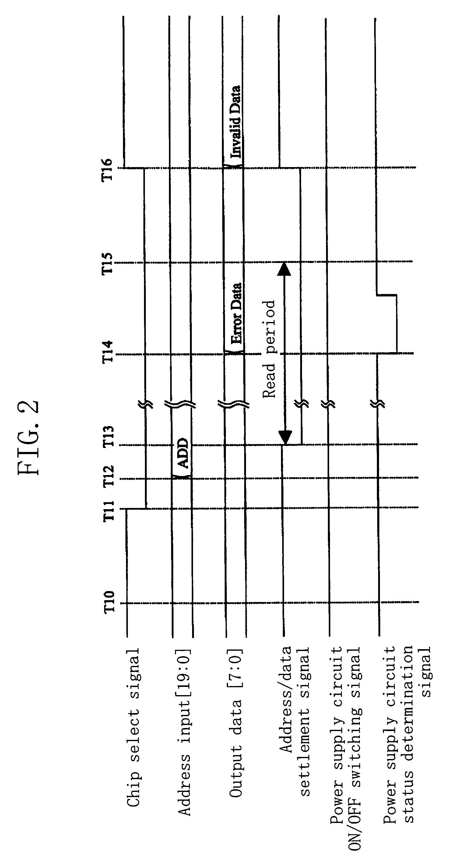
Incorporating a power supply circuit status determination circuit that suppresses the output of readout data when the power supply circuit is not operational, allowing data to be output via a common terminal and using error data to prevent control issues in data processing devices without additional signal lines.
Engineering Contradictions & Design Principles
Engineering Contradiction Analysis
1Reliability
If a dedicated terminal is added for outputting the ready_toRead signal, then the data processing device can be prevented from running out of control, but the total number of terminals increases
Solution Approach 1:
The patent applies multi-functionality by making the data output terminal serve dual purposes: it outputs both the ready_toRead signal and the data signal. The terminal acts as a universal interface that can carry different signals at different times, eliminating the need for a dedicated terminal while maintaining control stability.
Solution Approach 2:
The patent merges the function of the ready_toRead signal output with the data output function by using the same terminal for both purposes. This consolidation reduces the total number of terminals while ensuring that the data processing device receives appropriate control signals to prevent running out of control.
2Productivity
If data is output immediately after power supply voltage rises, then reading speed is improved, but erroneous data may be read out due to incomplete power supply circuit operation
Solution Approach 1:
The patent applies preliminary action by having the power supply circuit complete its initialization and stabilization before enabling data output. The ready_toRead signal is generated only after the power supply voltage has fully risen and the power supply circuit is confirmed to be operating normally, preventing erroneous data reading while maintaining efficient reading operations.
Solution Approach 2:
The patent uses feedback mechanisms where the power supply circuit status is monitored and fed back to control the data output enablement. The ready_toRead signal is generated based on feedback information about the power supply circuit's operational state, ensuring that data is only output when the power supply is fully operational and reliable.
Data Source

AI summary
A semiconductor memory device includes: a power supply circuit for outputting a power supply voltage used for reading out data; and a power supply circuit status determination circuit for determining whether an operation status of the power supply circuit is such that data can be read out normally. The output of readout data is suppressed while it is determined by the power supply circuit status determination circuit that the operation status is such that data cannot be read out normally.