
OLED Display TOF Sensing Layout for Compact 3D Gesture Detection
Find Innovative SolutionsGenerate Solutions
Solution Overview
Problem
Conventional 3D depth cameras are too large and expensive for integration with display panels, making it difficult to capture 3D spatial information and gesture recognition effectively due to the size and cost of silicon-based sensor arrays.
Innovation Solution
An integrated display apparatus with an OLED display panel that incorporates micro lenses and small array light-sensing chips on the backside, allowing for efficient detection of 3D spatial information and gesture recognition without obstructing the display area, using a surface-mount or transfer print process to attach light-sensing chips aligned with gaps between subpixels.
Engineering Contradictions & Design Principles
Engineering Contradiction Analysis
1Measurement precision
If conventional silicon-based sensor arrays are used for 3D depth detection, then measurement precision is improved, but device size and cost increase significantly
Solution Approach 1:
The patent divides the display panel into functional regions: display areas with subpixels and separate detection areas with light-sensing chips. This segmentation allows the sensing function to be performed by small, discrete chips rather than a large continuous sensor array, reducing overall device volume while maintaining detection precision.
Solution Approach 2:
The patent utilizes the vertical dimension by placing light-sensing chips on the backside of the display panel, aligned with gaps between subpixels. This three-dimensional integration allows simultaneous display and sensing functions without increasing the panel's footprint area, effectively reducing the device's horizontal volume.
2Measurement precision
If conventional silicon-based sensor arrays are used for 3D depth detection, then measurement precision is improved, but manufacturing cost increases
Solution Approach 1:
The patent merges the display panel and depth sensing functions into a single integrated device. The light-sensing chips are attached to the backside of the display panel using surface-mount or transfer print processes, combining two functions into one manufacturable unit and reducing overall system cost.
Solution Approach 2:
The patent employs small, low-cost light-sensing chips instead of expensive large-format silicon sensor arrays. These smaller chips are more economical to manufacture and can be produced in higher volumes, reducing the cost per unit while maintaining sufficient detection precision for gesture recognition applications.
3Device complexity
If light-sensing chips are integrated with display panel, then device complexity is reduced, but display area may be obstructed
Solution Approach 1:
The patent segments the panel into distinct display and detection areas, with light-sensing chips positioned in detection areas that correspond to gaps between subpixels. This segmentation ensures that the sensing chips do not obstruct the display area, as they are located in regions where no display elements exist.
Solution Approach 2:
The patent resolves the area conflict by utilizing the vertical dimension and gap spaces. Light-sensing chips are placed on the backside of the panel, aligned with gaps between front-side subpixels, effectively using three-dimensional space to accommodate both display and sensing functions without reducing the display area.
Applied Scientific Principles
This section explains which scientific principles are used to turn an abstract innovation direction into a practical engineering solution.
Function Achieved in This Case
Enables compact and cost-effective 3D spatial information detection and gesture recognition by reducing the size and number of light-sensing pixels, allowing for real-time data capture and processing of depth information without blocking the display panel.
Implementation Method 1
a light source disposed on the backside of the OLED display panel and configured to emit an infrared light signal
Implementation Method 2
a reflected infrared light signal from the target object
Implementation Method 3
The optical layer includes a plurality of micro lenses
Implementation Method 4
multiple light sensors respectively disposed under the back side of the optical layer and aligned with at least some of the multiple gaps, wherein each of the multiple light sensors is configured to detect the reflected infrared light signal
Implementation Method 5
depth information of a particular region of the target object based on time-of-fly information
Data Source
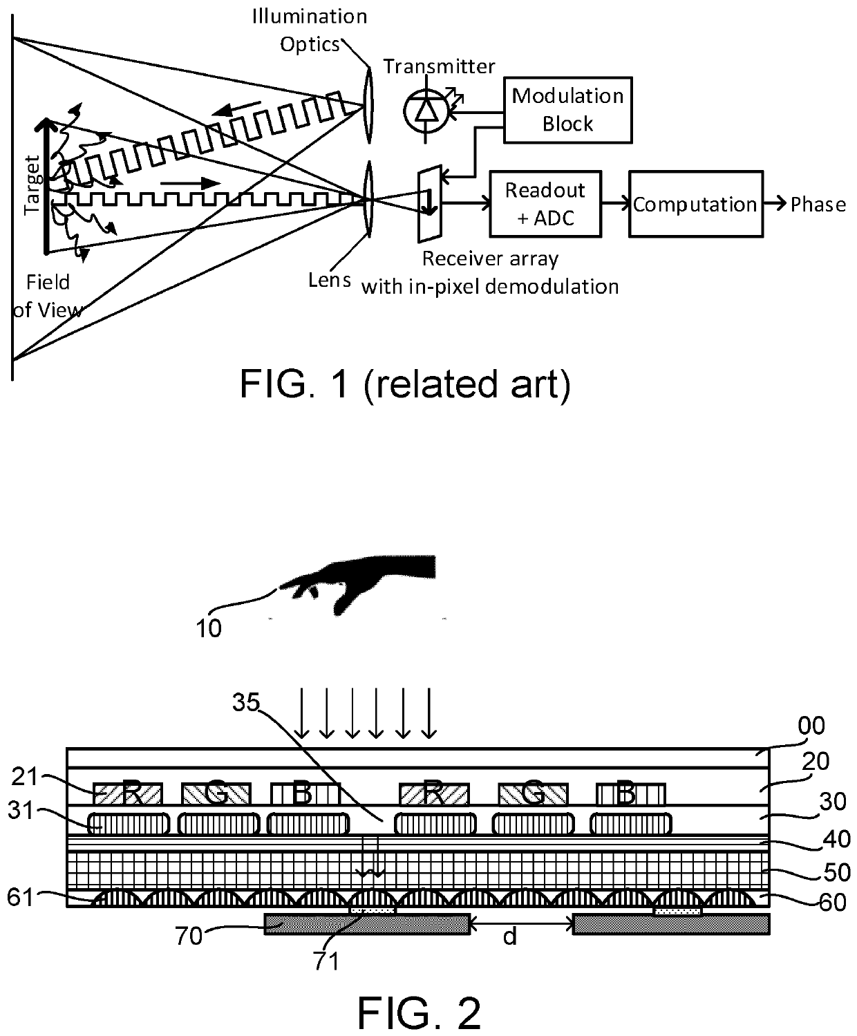 Figure 1~2
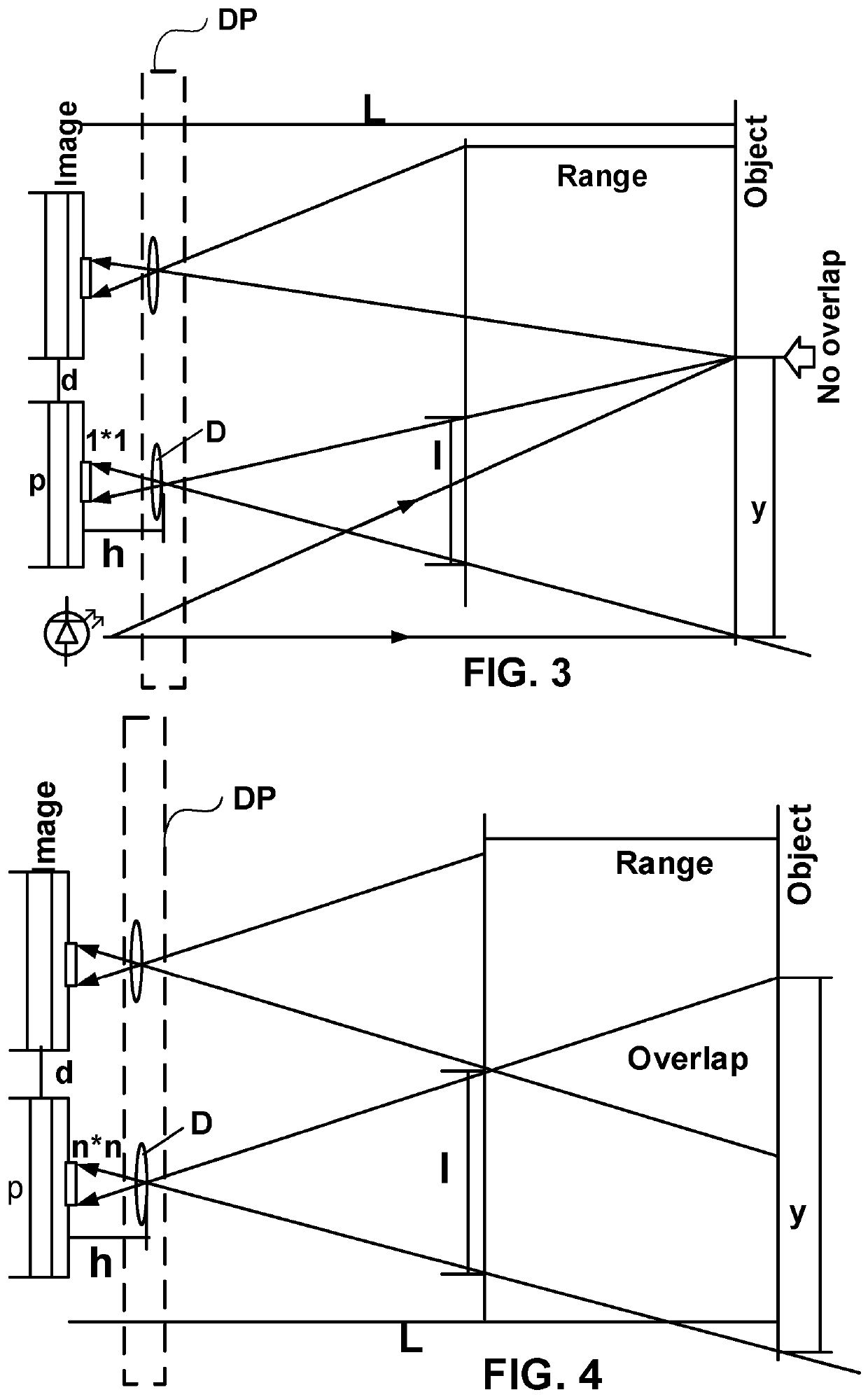 Figure 3~4
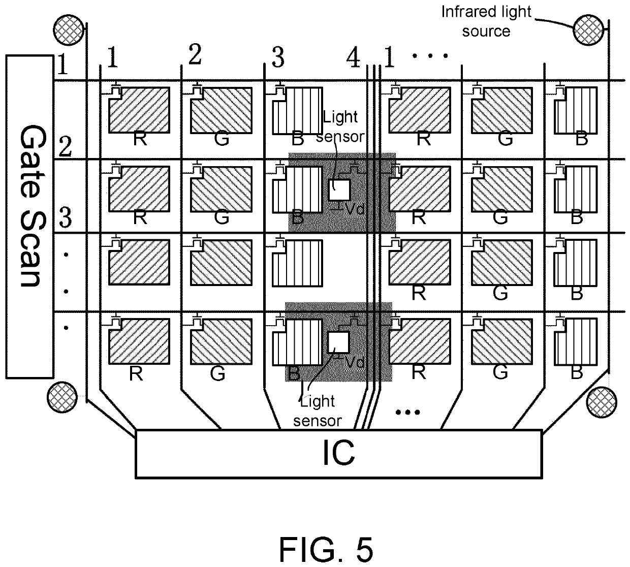 Figure 5
AI summary
A display apparatus for detecting three-dimensional (3D) spatial information. The display apparatus includes a display panel having a plurality of active subpixels in a display area configured with multiple gaps respectively between at least some active subpixels, the display panel including a counter substrate at front and a backplane substrate at back; an optical layer at a back side of the backplane substrate; multiple light sensors attached discretely on a back side of the optical layer and substantially aligned with the multiple gaps in the display area; and a light source on the backplane substrate and configured to provide an infrared light signal in a direction toward a field of view beyond the counter substrate. The multiple light sensors are configured to detect respective infrared light signals reflected from multiple different regions of an object in the field of view for collectively deducing 3D spatial information of the object.