
Temporary Adhesive Material for Wafer Processing
Find Innovative SolutionsGenerate Solutions
Solution Overview
Problem
Existing temporary adhesive materials for wafer processing lack compatibility with steps involving through silicon via (TSV) formation and wiring on the back surface, suffer from inadequate heat stability, and have limited productivity due to slow delamination processes and equipment requirements.
Innovation Solution
A temporary adhesive material comprising a first silicone-modified styrene base thermoplastic elastomer layer and a second thermosetting polymer layer, allowing for reversible adhesion to the wafer and substrate, enhancing compatibility with TSV and wiring formation, and enabling easy delamination with improved heat resistance and productivity.
Engineering Contradictions & Design Principles
Engineering Contradiction Analysis
1Reliability
If an organic resin film tape is used for protecting the wafer during grinding, then the wafer can be protected from breakage, but the tape lacks sufficient strength and heat resistance for TSV formation and wiring layer formation steps
Solution Approach 1:
The protective tape is divided into two distinct layers: a base material layer providing mechanical strength and heat resistance, and an adhesive layer providing protection during grinding. This segmentation allows each layer to be optimized for its specific function, enabling the composite tape to withstand both grinding forces and subsequent high-temperature TSV formation processes.
Solution Approach 2:
The protective tape is constructed as a composite material combining an inorganic or high-temperature resistant base material with a specially formulated adhesive layer. This composite structure provides both the mechanical protection needed during grinding and the thermal stability required for TSV formation and wiring layer formation at temperatures exceeding 200°C.
2Strength
If a silicone pressure sensitive adhesive is used for temporary adhesion, then the substrate can be bonded to the support, but the delamination process requires very long time and chemical agents, making it difficult to apply to production
Solution Approach 1:
The adhesive layer uses a thermoplastic polymer that changes its adhesive properties with temperature. At bonding temperature, it provides strong adhesion; at delamination temperature (higher than bonding temperature), it becomes less adhesive, enabling easy separation. This parameter change eliminates the need for chemical agents and significantly reduces delamination time.
Solution Approach 2:
The adhesive layer undergoes a phase transition when heated to the delamination temperature, changing from a sticky state to a less adhesive state. This phase transition allows the wafer to be easily separated from the support substrate without requiring solvents or extended processing time, making the process suitable for production environments.
3Ease of operation
If a heat-melting hydrocarbon-based compound is used as adhesive material, then bonding and delamination can be controlled by heating, but the adhesive does not have sufficient heat stability at temperatures higher than 200°C
Solution Approach 1:
The adhesive layer is formulated as a composite containing a thermoplastic polymer with high heat resistance (such as polyether block amide or polybutylene terephthalate) combined with processing aids. This composite structure maintains dimensional stability and adhesive properties at temperatures above 200°C while still allowing controlled delamination through heating, enabling compatibility with TSV formation processes.
4Loss of time
If light-absorbing substances are used in the adhesive for laser irradiation delamination, then the temporary adhesive layer can be decomposed, but expensive laser apparatus is required and processing time is extended
Solution Approach 1:
Instead of using light-absorbing substances requiring laser irradiation, the adhesive layer is designed to change its adhesive parameters through conventional heating. This approach achieves rapid delamination using simple thermal fields that are already present in semiconductor manufacturing equipment, eliminating the need for expensive laser apparatus while maintaining fast processing speeds.
Applied Scientific Principles
This section explains which scientific principles are used to turn an abstract innovation direction into a practical engineering solution.
Function Achieved in This Case
The solution facilitates high uniformity in film thickness, easy delamination, and increased productivity of thin wafers, allowing for efficient handling and reuse of substrates while maintaining heat resistance and solubility in hydrocarbon solvents.
Implementation Method 1
a first temporary adhesive layer composed of a layer (A) of a silicone-modified styrene base thermoplastic elastomer; and a second temporary adhesive layer composed of a thermosetting polymer layer (B) laminated on the first temporary adhesive layer, wherein the layer (A) is capable of releasably adhering to the front surface of the wafer
Implementation Method 2
the layer (B) is capable of releasably adhering to the supporting substrate
Data Source
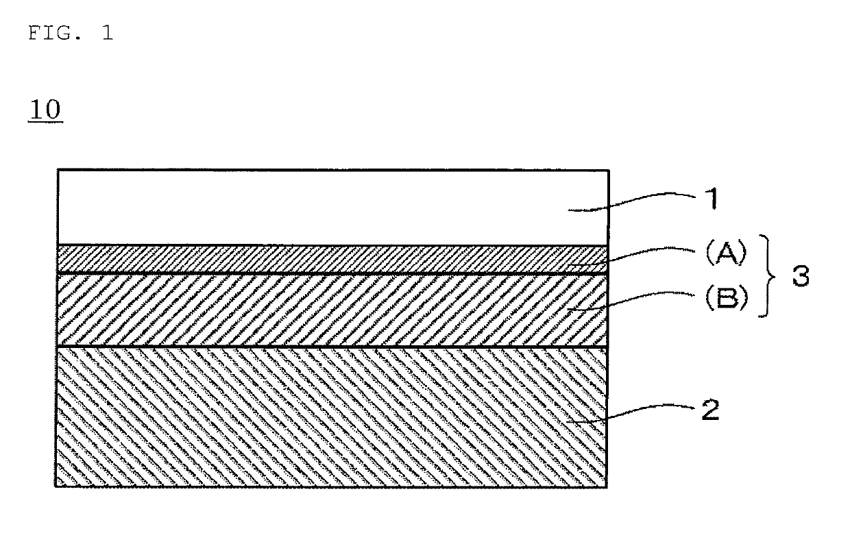 Figure 1

AI summary
The present invention is adhesive material for a wafer processing used for temporarily bonding a supporting substrate to a wafer having a front surface includes a circuit formed thereon and a back surface to be processed, including a first temporary adhesive layer composed of a layer (A) of a silicone-modified styrene base thermoplastic elastomer, and a second temporary adhesive layer composed of a thermosetting polymer layer (B) laminated on the first temporary adhesive layer, wherein the layer (A) is capable of releasably adhering to the front surface of the wafer, and the layer (B) is capable of releasably adhering to the supporting substrate. Thereby, there can be provided a temporary adhesive material for a wafer processing, a wafer processing lamination, and a method for manufacturing a thin wafer using the same, which facilitates temporary adhesion between a supporting substrate and a wafer having a circuit, is highly compatible with steps of forming a TSV and forming a wiring on the back surface of the wafer, allows easy delamination, and is capable of increasing productivity of thin wafers,