

01 Hot Tech and Product Updates
In this report, there is 1 news articles on the latest developments in the field of Semiconductor Epitaxy – Categories. These articles have been analyzed from 2 sides: the impact of technological innovations and their effects on users. From this analysis, we have summarized the following key points:
Tech Innovations
Single-Crystal-Like Germanium Substrate
The development of single-crystal-like germanium substrates is a key innovation that supports the use of flexible substrates while maintaining the desirable properties of single-crystal materials. This substrate is crucial for the epitaxial deposition of high-quality semiconductor films.
Epitaxial Deposition
This technique is central to the innovation discussed in the article. Epitaxial deposition allows for the precise placement of molecules on a substrate, ensuring that the crystallographic orientation is maintained. This is essential for the high-quality semiconductor films needed in advanced electronic devices.
Roll-to-Roll Manufacturing
This manufacturing process, likened to a printing press, is highlighted for its efficiency and cost-effectiveness. Roll-to-roll manufacturing allows for continuous processing of semiconductor materials, which can significantly reduce production costs and increase throughput.
Wide-Bandgap Semiconductors
Wide-bandgap semiconductors are crucial for applications requiring high temperature and power handling capabilities. They are typically more efficient than traditional silicon in these environments. The news article highlights the potential of these materials to replace silicon, indicating a significant shift in the materials used for high-performance electronics.
Flexible Substrates
The use of flexible, single-crystal-like germanium substrates represents a breakthrough in making semiconductors more adaptable to different applications, including potentially wearable electronics. Flexibility in substrates opens up new avenues for electronic devices that can conform to various shapes and surfaces.
Product Effects
Flexibility and Conformability
The flexible nature of the new semiconductor films allows for their use in innovative applications, such as flexible displays, wearable electronics, and medical devices that can conform to the human body.
Increased Power Load Handling
Devices built with these advanced semiconductors can handle increased power loads, making them suitable for more demanding applications, including power electronics and renewable energy systems.
Cost-Effectiveness
The roll-to-roll manufacturing process and the use of more readily available materials like germanium reduce the overall cost of semiconductor production. This makes the technology more accessible and could lead to broader adoption in various industries.
Large Area Coverage
The ability to produce semiconductor films over large areas is beneficial for applications like solar panels and large-area sensors. This capability can lead to more efficient energy capture and improved sensing technologies across extensive areas.
High-Temperature Operation
The use of wide-bandgap semiconductors enables devices to operate effectively at higher temperatures. This capability is critical for applications in harsh environments, such as automotive or industrial electronic systems.
Recommended News
Semiconductor advancement could lead to low-cost, flexible electronic devices
02 Technologies First Made Public
In this section, you will get the latest breakthroughs in four main technical directions of Semiconductor Epitaxy – Categories. These technologies, first made public, represent the cutting-edge innovations and progress in the solar cell industry, showcasing the potential and direction of future developments.
Metal Organic Chemical Vapor Deposition
| Metal Organic Chemical Vapor Deposition | View 2 First Tech |
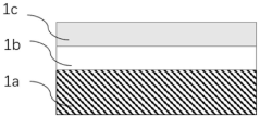
A kind of gallium oxide n-type doping method
Innovation: 1. The method of pulsed indium source and n-type dopant can improve the surface morphology of the gallium oxide film and prevent excessive accumulation of …
Technical Effect: The invention provides an n-type doping method for gallium oxide. By using a pulse method to introduce a reaction source, the surface morphology can be …
Technical Problem: The resistivity of the n-type gallium oxide film is high, the doping concentration cannot be accurately controlled, and the surface morphology of the grown …

A growth method for gallium oxide n-type doping
Abstract: The invention discloses a growth method of n-type doping of gallium oxide and a preparation technology of ε-phase gallium oxide. This solution is proposed to solve the problem of low preparation quality of n-type doping of ε-phase …
Metal Epitaxy
| Metal Epitaxy | View 2 First Tech |
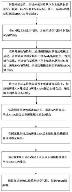
A kind of FBAR resonator preparation method and resonator
Innovation: This patent provides a method for preparing FBAR resonators. The method includes two steps: preparing an epitaxial substrate and etching an air cavity on …
Technical Effect: The invention provides a method for preparing an FBAR resonator by preparing an epitaxial substrate and etching an air cavity on a Si substrate, thereby …
Technical Problem: The existing thin film bulk acoustic resonator (FBAR) preparation method has the following problems: 1. The substrate material used in the existing method …
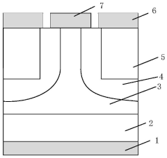
Gallium oxide Schottky diode based on mesa and floating metal ring composite terminals
Innovation: Introducing a composite terminal structure: By introducing a composite terminal structure of mesa and floating metal ring into the device, the voltage resist…
Technical Effect: The invention provides a gallium oxide Schottky diode based on a composite terminal of a mesa and a floating metal ring. By introducing a composite terminal …
Technical Problem: The voltage resistance performance and device reliability of existing gallium oxide devices are weak.
Heteroepitaxy
| Heteroepitaxy | View 2 First Tech |

Innovation: The radio frequency magnetron sputtering method is used to epitaxially grow β-Ga2O3 thin films on diamond substrates. This method has the ability to achieve …
Technical Effect: The invention provides a method for epitaxially growing a β-Ga2O3 thin film on a diamond substrate using a radio frequency magnetron sputtering method, there…
Technical Problem: The low thermal conductivity of β-Ga2O3 limits the power and frequency characteristics of electronic devices, causing power electronic devices manufactured …
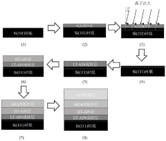
Preparation method of GaN material based on Si substrate with dielectric buffer layer protection
Innovation: First, a Si3N4 buffer layer is deposited on the Si substrate, and then ion implantation is used to form an array of micro-implantation pits on the surface of…
Technical Effect: The present invention deposits a Si3N4 buffer layer on the Si substrate and uses ion implantation to form an array of micro-injection pits on the surface of …
Technical Problem: How to pretreat Si substrate through ion implantation technology to improve the quality of GaN epitaxial layer.
Homoepitaxy
| Homoepitaxy | View 1 First Tech |
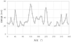
Epitaxial silicon wafer and manufacturing method thereof
Innovation: By growing homogeneous epitaxial layers in stages, the growth process of the epitaxial layer can be better controlled, thereby improving the flatness of the …
Technical Effect: The invention provides an epitaxial silicon wafer and a manufacturing method thereof, which can improve the flatness of the epitaxial silicon wafer.
Technical Problem: Poor flatness of epitaxial silicon wafers may cause out-of-focus, affect the chemical mechanical polishing process, and affect product yield.
| Strained Epitaxy |
03 Technical dynamic report in related fields
This section lists the latest updates from various fields, which will assist you to easily stay informed about the comprehensive progress of the industry and areas you might find interesting.
Semiconductor Epitaxy – Categories
Magnetic Resonance Imaging – Categories
Ultrasound Imaging – Categories
Photovoltaic Cells – Categories

