

01 Hot Tech and Product Updates
In this report, there is 1 news articles on the latest developments in the field of Semiconductor Deposition – Craft. These articles have been analyzed from 2 sides: the impact of technological innovations and their effects on users. From this analysis, we have summarized the following key points:
Tech Innovations
Spatial Atomic Layer Deposition (SALD)
The use of SALD technology by Nfinite Nanotech represents a significant innovation in the field of material science, particularly in the deposition of thin films. Unlike traditional Atomic Layer Deposition (ALD) that requires a vacuum environment, SALD allows for the deposition of atomically precise coatings in open air. This breakthrough not only simplifies the manufacturing process but also makes it more accessible and cost-effective for packaging manufacturers. The ability to integrate this technology into existing production lines without the need for specialized vacuum equipment is a game-changer, potentially leading to broader adoption and innovation in packaging solutions.
Compostable and Recyclable Materials
The focus on using compostable and recyclable materials for the base substrates that are enhanced by the nanocoating aligns with global sustainability goals. By improving the performance of these materials to match that of conventional plastics, Nfinite Nanotech is contributing to the reduction of plastic waste and promoting a circular economy. The fact that the final packaging can be either composted or recycled highlights the commitment to environmental responsibility while addressing consumer and regulatory demands for more sustainable packaging options.
Nanocoating
Nfinite Nanotech has leveraged the potential of nanotechnology to develop an ultra-thin coating that significantly enhances the barrier properties of various materials including paper, compostable biopolymers, and recyclable plastics. This advancement addresses the critical challenge in the packaging industry of finding sustainable yet effective alternatives to fossil-derived plastics. The nanocoating’s ability to block moisture and air extends the usability of greener materials for food packaging, which traditionally could not withstand such environmental factors for extended periods.
Product Effects
Manufacturing Flexibility
The flexibility of the nanocoating to withstand additional manufacturing processes without degradation is crucial for commercial scalability. This allows manufacturers to tailor the application of the nanocoating to specific product needs and production environments, enhancing the adaptability and appeal of this technology in diverse market segments.
Sustainability
The nanocoating’s compostable and recyclable properties ensure that the end products contribute to sustainability. This aligns with increasing regulatory pressures and consumer demand for environmentally friendly products. The ability to dispose of the packaging sustainably or repurpose it without contributing to landfill waste is a significant advantage.
Antimicrobial and UV Resistance
The antimicrobial properties of the nanocoating improve food safety by reducing the risk of microbial growth, which can lead to food spoilage. Additionally, resistance to UV light helps in preserving the integrity and quality of the packaged goods, particularly those sensitive to light exposure. These properties ensure that the food remains safe and of high quality throughout its extended shelf life.
Extended Shelf Life
The primary efficacy of Nfinite’s nanocoating is its ability to extend the shelf life of food products. By providing a robust barrier against moisture and oxygen, the coated materials can preserve food for longer periods, reducing food waste and enhancing the economic viability of using sustainable packaging materials in the food industry.
Recommended News
Eco-friendly nanocoatings for food packaging
02 Technologies First Made Public
In this section, you will get the latest breakthroughs in four main technical directions of Semiconductor Deposition – Craft. These technologies, first made public, represent the cutting-edge innovations and progress in the solar cell industry, showcasing the potential and direction of future developments.
Chemical Vapor Deposition
| Chemical Vapor Deposition | View 29 First Tech |
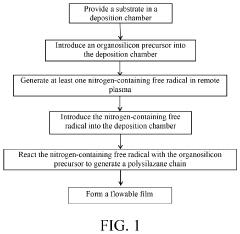
Method for forming high-quality film by CVD process
Abstract: This application relates to a method for forming a high-quality film by a CVD process. Specifically, this application provides a method for depositing a flowable film on a substrate. The method includes: introducing an organosilicon …

Innovation: This patent proposes a chemical vapor phase reaction device for semiconductors and pan-semiconductors based on microvalve mass flow control. The chemical …
Technical Effect: The invention is a chemical gas phase reaction device for semiconductors and pan-semiconductors based on microvalve mass flow control. Its technical effect …
Technical Problem: Traditional sprinkler injectors have the following problems in gas flow control: 1. It is impossible to achieve precise and adjustable mass flow control for …
Metal Organic Chemical Vapor Deposition
| Metal Organic Chemical Vapor Deposition | View 23 First Tech |
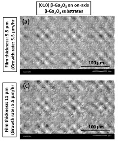
Compositions comprising aluminum and/or gallium oxide on a miscut substrate, and methods of making and use thereof
Innovation: The use of a miscut substrate, which can improve the crystal quality and reduce defects in the deposited layer. The specific composition of the deposited …
Technical Effect: The patent text describes a composition comprising a layer of P-(AlxGai-x)2O3 disposed on a miscut substrate of P-(AlzGai-z)2O3. The composition aims to …
Technical Problem: The technical problem addressed in this patent is the need for compositions and devices with improved properties.
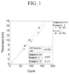
Innovation: The use of a thermally stable metal oxide thin film precursor. The ability of the precursor to be reliably used in a deposition process.
Technical Effect: The patent text describes a metal oxide thin film precursor that is thermally stable and can be used in a deposition process. The precursor is used to form a…
Technical Problem: The current performance of the dielectric layer (metal oxide thin film) for a semiconductor device does not meet the needs of the market.
Physical Vapor Deposition
| Physical Vapor Deposition | View 17 First Tech |
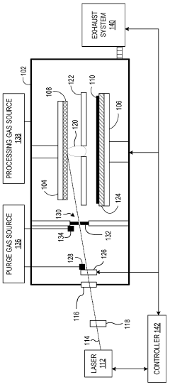
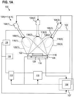
Reducing particle contamination of a laser entrance window in a pulsed laser deposition tool
Innovation: The introduction of a purge gas inlet located between the laser entrance window and the target holder. this inlet is configured to direct a flow of purge …
Technical Effect: The technical efficacy of the patent text is that it describes a pulsed laser deposition (PLD) tool that includes a purge gas inlet located between the …
Technical Problem: The technical issues addressed in this patent text are related to reducing particle contamination on a laser entrance window of a pulsed laser deposition tool.
Devices and methods for sputtering at least two elements
Innovation: The use of a sputtering method to deposit a material layer with a predefined stoichiometry. The ability to control the atomic ratio between at least two …
Technical Effect: The patent technology allows for the generation of a material layer with a predefined atomic ratio between at least two elements.
Technical Problem: The technical issue is that when depositing material layers using sputtering, the stoichiometry of the deposited layer may not be accurately controlled.
Atomic Layer Deposition
| Atomic Layer Deposition | View 15 First Tech |
Innovation: This patent proposes a chemical vapor phase reaction device for semiconductors and pan-semiconductors based on microvalve mass flow control. The chemical …
Technical Effect: The invention is a chemical gas phase reaction device for semiconductors and pan-semiconductors based on microvalve mass flow control. Its technical effect …
Technical Problem: Traditional sprinkler injectors have the following problems in gas flow control: 1. It is impossible to achieve precise and adjustable mass flow control for …
Metal-oxide blocking layers deposited via atomic layer deposition for organic light emitting diodes
Innovation: The use of metal oxide blocking layers in oleds to improve device performance and stability. The specific materials used for the metal oxide blocking layers,…
Technical Effect: The technical efficacy of the patent text is the use of metal oxide blocking layers in organic light emitting diodes (OLEDs) to improve device performance …
Technical Problem: The technical issues addressed in this patent text are related to the performance and stability of organic light emitting diodes (OLEDs). Specifically, the …
| Liquid Phase Deposition | View 1 First Tech |
03 Technical dynamic report in related fields
This section lists the latest updates from various fields, which will assist you to easily stay informed about the comprehensive progress of the industry and areas you might find interesting.
Wafer – Preparation Crafts
Semiconductor Cleaning
Semiconductor Etching – Craft