

01 Hot Tech and Product Updates
In this report, there is 1 news articles on the latest developments in the field of Semiconductor Etching – Craft. These articles have been analyzed from 2 sides: the impact of technological innovations and their effects on users. From this analysis, we have summarized the following key points:
Tech Innovations
Sub-10-micron Micro-bump Structures
Allows for tighter packing of transistors, significantly increasing the density and thereby the performance of semiconductor chips, crucial for high-performance computing tasks.
Vacuum-based Single Wafer Processing
Enhances the reliability of semiconductor devices by reducing oxidation and other defects that can arise during the reflow process, crucial for maintaining high yields in production.
Proprietary Algorithms
Enhance the efficiency and effectiveness of the tuning process in plasma etching, reducing the time and cost associated with semiconductor manufacturing.
Multilevel Pulse States
Facilitates the etching process to accommodate complex and delicate patterns required in modern semiconductor devices, supporting the development of multi-layered semiconductor architectures.
3D Stacking
Enables the integration of higher computing power within a smaller footprint, crucial for AI-driven applications like large language models, enhancing performance and efficiency.
RF-Synchronized Tuning
Provides precise control over plasma characteristics, essential for etching intricate designs on semiconductors without causing damage to the material, thus maintaining functionality and reliability.
Single Wafer Chamber Design
Improves the uniformity and quality of the semiconductor manufacturing process, addressing the challenges posed by smaller geometries in advanced semiconductor designs.
Product Effects
Ultra-Fast Response
Ensures that adjustments in the manufacturing process can be made swiftly and accurately, reducing waste and increasing the efficiency of the production line.
Extended Technology to Sub-10um Pitch
Demonstrates the capability of the technology to keep pace with the rapid advancements in semiconductor miniaturization, essential for the next generation of electronic devices.
Minimized Inter-metallic Compound Zones
Reduces potential points of failure in semiconductor devices, enhancing their durability and lifespan, which is critical for devices requiring high reliability.
Superior Quality and Total Cost of Ownership (CoO)
Indicates that the technology not only improves the performance and reliability of semiconductor components but also reduces the cost associated with their production, making advanced technologies more accessible.
High Throughput and Low CoO
Suggests a streamlined production process that allows for the mass production of high-quality semiconductor devices at a lower cost, crucial for meeting the growing demand in various technology sectors.
Compatibility with IoT Platforms
Allows for the integration of semiconductor devices with smart technologies, facilitating better monitoring and optimization of performance across various applications, enhancing usability and functionality.
Recommended News
YES Delivers Multiple VeroTherm Formic Acid Reflow Systems To Leading Semiconductor Device Customers
Dual drug delivery platforms for bone tissue engineering
02 Technologies First Made Public
In this section, you will get the latest breakthroughs in four main technical directions of Semiconductor Etching – Craft. These technologies, first made public, represent the cutting-edge innovations and progress in the solar cell industry, showcasing the potential and direction of future developments.
Plasma Etching
| Plasma Etching | View 38 First Tech |
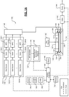
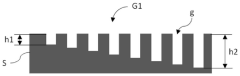
Lower plasma exclusion zone ring for controlling plasma deposition or etching near a substrate notch
Innovation: The use of a lower plasma exclusion zone ring to control plasma deposition or etching near a substrate notch. The design of the ring to optimize plasma …
Technical Effect: The technical efficacy of the patent text is the inclusion of a lower plasma exclusion zone ring for a substrate processing system. This ring helps to …
Technical Problem: The technical issues addressed in this patent text are related to the control of plasma deposition or etching near a substrate notch.
Methods for reducing leakage current
Innovation: The patent solution focuses on reducing leakage current in structures made up of different layers on a semiconductor wafer. The innovation lies in the method…
Technical Effect: The patent technology provides a method for reducing leakage current in semiconductor devices. By optimizing the device structure and material composition, …
Technical Problem: The technical problem addressed in this patent is the reduction of leakage current in semiconductor devices.
Wet Etching
| Wet Etching | View 10 First Tech |
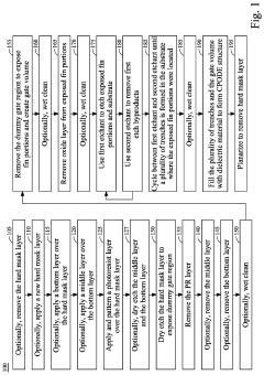
A method for preparing trench power devices
Innovation: By changing the etching method of the gate polysilicon, the concave horn morphology of the original gate polysilicon after etching is avoided, and the …
Technical Effect: By utilizing the photoresist step coverage capability, the gate electrode is formed by etching polysilicon combined with photoresist, thereby avoiding the …
Technical Problem: In the SGT process, the concave horn shape after the gate polysilicon is etched back will cause the electric field to accumulate, increase the IGSSR current,…
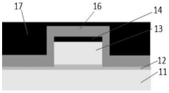
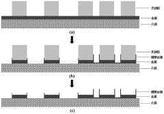
A method of manufacturing a MIM capacitor structure
Innovation: In the original MIM capacitor manufacturing process, by adding a wet etching step, the damaged dielectric layer is eliminated, the leakage path is blocked, a…
Technical Effect: By adding a wet etching step to the existing MIM capacitor manufacturing process, the present invention realizes that the damaged dielectric layer is exclude…
Technical Problem: During the manufacturing process of MIM capacitors, plasma etching can cause damage to the edges of the dielectric layer, which in turn leads to problems …
Ion Beam Sputtering Etching
| Ion Beam Sputtering Etching | View 8 First Tech |
Ion beam etching device and method, baffle mechanism and device for processing gratings
Innovation: Control mechanism configuration. The control mechanism is configured to control the movement of the baffle perpendicularly to the first direction while the …
Technical Effect: The present invention provides an ion beam etching device and method, a baffle mechanism for the ion beam etching device, and a device for processing a …
Technical Problem: In the prior art, the gradient of grating depth requires complex processing techniques to be achieved.
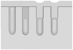
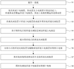
A kind of manufacturing method and manufacturing system of semiconductor device
Innovation: This patent provides a method for manufacturing a semiconductor device, by using a first target gas to etch a metal layer of a target thickness using a mask …
Technical Effect: This patent document relates to a method and manufacturing system for manufacturing semiconductor devices. Its technical effect is to increase the etching …
Technical Problem: When manufacturing semiconductor devices, when the etching process is used for pattern transfer, the dense mask layer pattern results in a high aspect ratio,…
Reactive Ion Etching
| Reactive Ion Etching | View 5 First Tech |
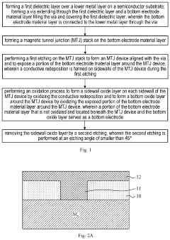
Methods for fabricating magnetoresistive random access memory
Innovation: The use of a sidewall oxide layer to reduce the risk of short-circuit points in the mram device, and the specific oxidation process used to form the sidewall…
Technical Effect: The technical efficacy of the patent text is to provide methods for fabricating a magnetoresistive random access memory (MRAM) device with reduced risk of …
Technical Problem: In advanced process nodes for MRAM devices, the small pitch arrangement of multiple MTJ components on a semiconductor substrate leads to a problem caused by …
Nano-Josephson junction and superconducting device and manufacturing method thereof
Innovation: The invention provides a method for producing nano-Josephson junctions, through which nano-size Josephson junctions can be prepared, thereby improving the in…
Technical Effect: The invention provides a method for manufacturing a nano-Josephson junction, through which a nano-sized Josephson junction can be prepared, thereby improving…
Technical Problem: The current photolithography equipment limits the preparation of smaller-sized Josephson junctions, which severely limits the integrated circuits, work …
03 Technical dynamic report in related fields
This section lists the latest updates from various fields, which will assist you to easily stay informed about the comprehensive progress of the industry and areas you might find interesting.
Wafer – Preparation Crafts
Semiconductor Cleaning
Semiconductor Deposition – Craft
Solid State Battery – Manufacturing Processes