

01 Hot Tech and Product Updates
In this report, there are 3 news articles on the latest developments in the field of Semiconductor Etching – Thin Film Materials. These articles have been analyzed from 2 sides: the impact of technological innovations and their effects on users. From this analysis, we have summarized the following key points:
Tech Innovations
Sub-10-micron Micro-bump Structures
Allows for the creation of extremely fine interconnects between stacked chips, crucial for reducing latency and increasing bandwidth. Enhances the efficiency and speed of memory and logic chip communication, critical for high-performance computing applications.
Vacuum-based Single Wafer Processing
Enhances the cleanliness and precision of solder reflow processes by operating in a controlled vacuum environment. Leads to higher yield rates and reliability in semiconductor production, essential for advanced technology applications.
Multilevel Pulse States
Enables precise control over plasma characteristics during complex etching processes by adjusting to different energy levels. Allows for the fabrication of intricate semiconductor structures, enhancing the functionality and miniaturization of electronic devices.
3D Stacking
Enables denser packaging and integration of chips, crucial for the compact and efficient design of AI accelerators. Directly impacts the performance capabilities of AI systems, particularly those using large language models, by improving processing speed and data handling.
Multilevel Pulse States
Enables precise control over plasma characteristics during complex etching processes by adjusting to different energy levels. Allows for the fabrication of intricate semiconductor structures, enhancing the functionality and miniaturization of electronic devices.
RF-Synchronized Tuning
Allows for real-time adjustments to the impedance matching network, synchronizing with the generator for optimal plasma control. Improves the accuracy and repeatability of semiconductor etching processes, essential for maintaining tight production tolerances.
Single Wafer Chamber Design
Provides tailored environments for individual wafers, improving the consistency and quality of the reflow process. Reduces defects such as bump cracking and collapsed bumps, crucial for maintaining the integrity of micro-scale architectures.
Product Effects
Extended Technology to Sub-10um Pitch
The ability to work with sub-10um pitches opens up possibilities for further miniaturization of semiconductor devices, pushing the boundaries of current technology.
Superior Quality and Total Cost of Ownership (CoO)
Ensures that the manufacturing processes not only yield high-quality results but also remain cost-effective, balancing performance with economic viability.
Minimized Reflected Power
Reducing reflected power in plasma processes leads to more precise etching, crucial for the fabrication of defect-free semiconductor structures.
Enhanced Bone Regeneration
By effectively delivering therapeutic agents directly to the site of injury, these platforms significantly improve the outcomes of bone repair and regeneration, crucial for medical advancements in orthopedics.
High Throughput and Low CoO
Achieving high throughput while maintaining low operational costs is crucial for competitive manufacturing, ensuring high productivity without compromising on cost.
Recommended News
YES Delivers Multiple VeroTherm Formic Acid Reflow Systems To Leading Semiconductor Device Customers
Dual drug delivery platforms for bone tissue engineering
02 Technologies First Made Public
In this section, you will get the latest breakthroughs in four main technical directions of Semiconductor Etching – Thin Film Materials. These technologies, first made public, represent the cutting-edge innovations and progress in the solar cell industry, showcasing the potential and direction of future developments.
Polycrystalline Silicon Film
| Polycrystalline Silicon Film | View 19 First Tech |
Semiconductor structure, solar cell and manufacturing method thereof, photovoltaic module
Innovation: By adjusting the extinction coefficient k of the N-type doped polysilicon layer and the P-type doped polysilicon layer, N-type doped polysilicon layers and …
Technical Effect: The invention provides a solar cell. By adjusting the extinction coefficient k of the N-type doped polysilicon layer and the P-type doped polysilicon layer, …
Technical Problem: The electrode slurry used to make the positive electrode and the negative electrode in existing solar cells usually have different compositions to ensure …

Semiconductor device, manufacturing method thereof and method for removing residual polysilicon
Innovation: By forming a third silicon dioxide layer at the bottom of the trench, and removing the remaining polysilicon layer on the sides of the trench through an etch…
Technical Effect: The present invention provides a method for manufacturing a semiconductor device, which can ensure the flatness of the bottom of the trench and at the same …
Technical Problem: During the formation process of germanium (Ge) epitaxial trenches, how to effectively remove the polysilicon layer at corresponding locations to avoid the …
Silicon Dioxide Film
| Silicon Dioxide Film | View 6 First Tech |
Semiconductor device, manufacturing method thereof and method for removing residual polysilicon
Innovation: By forming a third silicon dioxide layer at the bottom of the trench, and removing the remaining polysilicon layer on the sides of the trench through an etch…
Technical Effect: The present invention provides a method for manufacturing a semiconductor device, which can ensure the flatness of the bottom of the trench and at the same …
Technical Problem: During the formation process of germanium (Ge) epitaxial trenches, how to effectively remove the polysilicon layer at corresponding locations to avoid the …
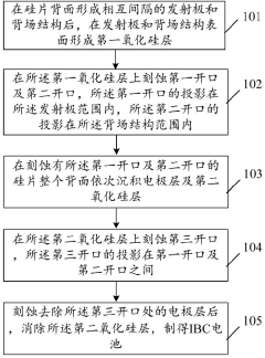
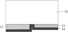
An IBC battery and its preparation method
Innovation: By forming mutually spaced emitter and back field structures on the back of the silicon wafer, forming a first silicon oxide layer on the surface, forming …
Technical Effect: The invention provides a method for preparing an IBC battery. The IBC battery prepared by the method has high efficiency performance.
Technical Problem: Currently, there are technical problems in the preparation of IBC batteries, and it is impossible to efficiently form contact electrodes on the back of IBC …
Silicon Nitride Film
| Silicon Nitride Film | View 6 First Tech |
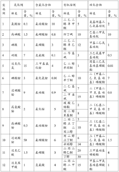
Etching composition and use thereof
Innovation: A specific etching composition is used, which includes an oxidizing agent, a fluorine-containing compound, a silicon compound, an organic solvent, and water….
Technical Effect: The present invention provides an etching composition that can selectively remove silicon germanium and adjust the etching selectivity ratio while avoiding …
Technical Problem: When manufacturing integrated circuits, how to effectively remove silicon germanium and control the etching selectivity while avoiding etching of other …
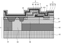
Semiconductor structures and manufacturing methods
Innovation: By using a contact hole etch stop layer including a tensile stress silicon nitride layer, a contact field plate is formed in a field plate contact hole …
Technical Effect: Embodiments of the present disclosure solve the additional problem in the contact field plate process by using a contact hole etch stop layer including a …
Technical Problem: When manufacturing the contact field plate structure in a BCD device, the additional contact field plate process will lead to the introduction of additional …
Metal Films
| Metal Films | View 5 First Tech |
Etch stop for oxide semiconductor devices
Innovation: By introducing an etch stop layer, the etching process of oxide semiconductor devices can be effectively controlled, thereby improving the performance and …
Technical Effect: This patent document relates to an etching stop technology for oxide semiconductor devices, the technical effect of which is to improve the performance and …
Technical Problem: As the size of integrated circuits continues to shrink, the manufacturing of TFT structures faces many challenges, including reductions in film thickness and…

Technical Effect: The invention provides a patterned conductive compensation substrate, a perovskite battery module and a preparation method thereof. By depositing conductive …
Technical Problem: During the preparation process of existing perovskite solar cell modules, there are problems such as inconsistent laser etching depth, chipping and peeling …
03 Technical dynamic report in related fields
This section lists the latest updates from various fields, which will assist you to easily stay informed about the comprehensive progress of the industry and areas you might find interesting.
Lithium Battery – Materials
Sodium-ion Battery – Materials
Solid State Battery – Materials