
Introduction
When designing circuits, choosing the right transistor is crucial for achieving optimal performance and efficiency. Two of the most common options are NMOS vs. PMOS transistors, each offering distinct advantages depending on the application. While NMOS transistors are known for their speed and efficiency, PMOS transistors excel in specific roles that require low power consumption and certain circuit configurations. This article will explore the key differences, benefits, and considerations to help you determine which transistor is the best fit for your circuit design needs.
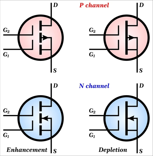
What Are NMOS Transistors
Definition and Principle
- What Are NMOS Transistors? NMOS transistors are widely used in digital and analog circuits for amplifying or switching electronic signals.
- Key Components: They consist of n-type and p-type semiconductor regions. The n-type regions are doped with donor impurities, while the p-type regions are doped with acceptor impurities.
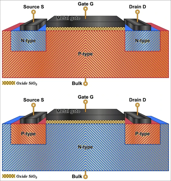
- Basic Structure: The design includes an n-type source and drain on either side of a p-type channel. A gate, separated from the channel by a dielectric material like silicon dioxide, controls the transistor’s operation.
How NMOS Transistors Operate
- Voltage Control: Applying a specific voltage to the gate with respect to the source creates an n-type conduction channel. This channel allows current to flow between the drain and the source.
- Low Voltage Applications: NMOS transistors are ideal for low voltage circuits, offering low resistance and high current capacity. These characteristics make them a popular choice in many modern electronic designs.
What Are PMOS Transistors
Definition and Structure
- Core Components: A PMOS transistor includes three primary regions: the source, drain, and channel. The channel connects the source and drain, serving as the pathway for current flow.
- Gate Control: The gate electrode, insulated from the channel by a gate dielectric, regulates the current flow.
- Charge Carriers: PMOS transistors use holes, or positive charge carriers, for current conduction. This distinguishes them from NMOS transistors, which rely on electrons.
Working Principle
- Voltage-Driven Operation: The PMOS transistor operates based on the voltage applied to the gate relative to the source (VGS).
- Conduction State: When VGS is more negative than the threshold voltage, the channel inverts, allowing holes to flow from the source to the drain. This enables current conduction.
- Cutoff State: When VGS is more positive than the threshold voltage, the channel depletes, and the transistor turns off, stopping current flow.
NMOS vs. PMOS: Key Differences
1. Construction and Principle of Operation
- NMOS Transistors: NMOS devices use electrons as the majority carriers to create an N-type channel between the source and drain. A positive gate voltage relative to the source forms the conduction channel, allowing current to flow.
- PMOS Transistors: PMOS devices rely on holes as the majority carriers to create a P-type channel between the source and drain. A negative gate voltage relative to the source enables current conduction.
2. Switching Speed
- NMOS transistors operate faster than PMOS because electrons move more quickly through silicon than holes. This speed advantage makes NMOS ideal for high-performance applications.
3. Power Consumption and Efficiency
- NMOS Efficiency: NMOS transistors consume less power, particularly at higher frequencies, making them more energy-efficient.
- PMOS Noise Immunity: PMOS devices offer better noise immunity at high frequencies, which can be advantageous in sensitive applications.
4. Voltage Handling and Dropout Characteristics
- Low Dropout Voltage in PMOS: PMOS transistors handle lower dropout voltages effectively, making them suitable for low-power applications.
- Higher Output Power in NMOS: NMOS devices excel in output power and efficiency but may lack the low-power benefits PMOS provides in specific scenarios.
5. Noise Performance
- Lower Noise in PMOS: PMOS transistors exhibit lower flicker noise, which benefits CMOS imagers and low-noise designs.
- Dark Current in NMOS: NMOS devices can show higher dark current levels, which may limit their use in applications like night vision and scientific imaging.
6. Reliability and Sensitivity
- Plasma Damage Concerns: NMOS and PMOS transistors differ in their sensitivity to plasma damage during manufacturing.
- Optimized Fabrication: Techniques like stress memorization dielectrics can enhance NMOS reliability without compromising PMOS performance.
7. Applications
- NMOS Use Cases: NMOS transistors are ideal for high-speed, low-power applications like digital logic circuits and high-performance computing.
- PMOS Use Cases: PMOS devices are better suited for applications requiring low dropout voltage and noise immunity, such as analog circuits and power management systems.
Choosing the Right Transistor for Your Design
Prioritize Switching Speed
- Best for Speed: If your design requires fast operation, NMOS transistors are ideal due to their superior switching speed.
- Applications: Use NMOS in digital logic circuits, processors, and high-performance computing where quick response is critical.
Evaluate Power Efficiency
- Energy-Saving Needs: For energy-efficient designs, NMOS transistors typically consume less power, especially at higher frequencies.
- Noise Considerations: If your application needs better noise immunity, PMOS transistors may perform better, even with slightly higher power consumption.
Assess Voltage Requirements
- Low Power Scenarios: PMOS transistors are excellent for low-power applications because they handle minimal dropout voltage effectively.
- High Power Needs: NMOS transistors often provide better output power and efficiency, making them suitable for high-power systems.
Consider Noise Sensitivity
- Low Noise Solutions: PMOS transistors excel in applications requiring minimal flicker noise, such as CMOS imagers and analog circuits.
- Efficiency Over Noise: For designs where noise is less of a concern, NMOS transistors deliver better overall performance and speed.
Match the Transistor to the Application
- Digital Designs: NMOS transistors are best for high-speed, low-power digital circuits.
- Analog and Power Management: PMOS transistors are more suitable for analog circuits, power management systems, and applications needing higher noise immunity.
To get detailed scientific explanations of NMOS vs. PMOS, try Patsnap Eureka.
