

01 Hot Tech and Product Updates
We have handpicked 3 news articles on the latest developments in the field of Semiconductor Packaging – Typical Technologies. These articles have been analyzed from 2 sides: the impact of technological innovations and their effects on users. From this analysis, we have summarized the following key points:
Tech Innovations
FOWLP (Fan-Out Wafer Level Packaging)
Influence on Technology: FOWLP has been a stepping stone in the evolution of packaging technologies, providing a foundation for the development of FOPLP. It has been utilized in high-performance applications like the iPhone 7’s A10 processor, showcasing its capability for high-density integration and improved electrical performance.
3D Integration
Influence on Technology: 3D integration technology, facilitated by advancements in materials like 2D semiconductors, allows for more compact and efficient integrated circuits. This technology is essential for enhancing chip-level energy efficiency and functionality, meeting the needs of next-generation computing demands.
TGV (Through Glass Vias)
Influence on Technology: The development of TGV technology by companies like YES enhances the capabilities of glass substrates in semiconductor packaging. This technology supports the creation of high aspect ratio vias necessary for advanced 2.5D and 3D packaging, crucial for AI and high-performance computing applications.
Heterogeneous Integration
Influence on Technology: Heterogeneous integration involves the packaging of multiple different types of chips into a single package. This approach is enabled by technologies like FOPLP and FOWLP, allowing for the integration of diverse functionalities and improving overall device performance.
2D Materials (Transition Metal Dichalcogenides, Graphene)
Influence on Technology: 2D materials are pivotal in transcending the limitations of traditional silicon-based technologies. Their unique properties enable ultra-thin, high-performance transistors and the potential for monolithic 3D integration, which could revolutionize information technology and extend Moore’s Law.
AI GPU (Artificial Intelligence Graphics Processing Unit)
Influence on Technology: The transition of AI GPU packaging from 2.5D wafer level to panel level under FOPLP and FOWLP technologies aims to accommodate larger chip sizes and potentially reduce costs. This is crucial for supporting the computational demands of AI applications, including large language models and advanced AI algorithms.
Product Effects
High reliability and quality
The development of technologies like TGV for through glass vias ensures high reliability and quality in semiconductor manufacturing, essential for applications in advanced packaging and AI.
Enhanced performance and functionality
The use of advanced materials like 2D semiconductors and innovative packaging technologies like 3D integration enhances the performance and functionality of semiconductor devices, meeting the increasing demands of modern applications.
Advanced manufacturing capabilities
Innovations in semiconductor packaging, such as the use of FOPLP and the integration of 2D materials, demonstrate advanced manufacturing capabilities that drive the industry forward, enabling the production of more sophisticated and efficient devices.
Improved thermal management
Technologies such as TGV and materials like graphene improve thermal management in semiconductor devices, which is critical for maintaining performance and reliability in high-power and high-performance applications.
Larger packaging sizes
The transition to panel-level packaging allows for larger sizes, which is beneficial for applications requiring larger chips, such as AI GPUs. This can lead to improved performance due to the integration of more functionalities within a single package.
Recommended News
YES Panel-Level Through Glass Via (TGV) Etch Tool Placed in Production
Next-gen semiconductors: 7-year roadmap for 2D materials integration
02 Technologies First Made Public
In this mail, we have filtered out the latest breakthroughs in four main technical directions of Semiconductor Packaging – Typical Technologies. These technologies, first made public, represent the cutting-edge innovations and progress in the solar cell industry, showcasing the potential and direction of future developments.
2.5D/3D Packaging
| 2.5D/3D Packaging | View 8 First Tech |
A three-dimensional stacked structure and its testing method
Innovation: The first test object chain contains different types of test objects, and the distance between test objects at the same level in different chains and the ref…
Technical Effect: This patent text describes a three-dimensional stacked structure and its testing method. By setting a first test structure in the three-dimensional stacked s…
Technical Problem: How to effectively test the impact of the TSV process on surrounding devices in a three-dimensional stacked structure.
Innovation: Provides an integrated architecture data bus to realize data interaction and sharing between various functional modules in shipbuilding industry software The…
Technical Effect: The invention provides basic public services and standardized interfaces, reduces the technical requirements of software producers in the development and int…
Technical Problem: When the functions and scale of shipbuilding industry software increase, there are problems such as poor software integration and serious information islanding.
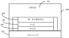
Ball Grid Array (BGA)
| Ball Grid Array (BGA) | View 8 First Tech |
Innovation: The use of a first substrate with a first surface extending in a first direction and a second surface extending in a second direction. this allows for increa…
Technical Effect: The technical efficacy of the patent text is that it describes a semiconductor package that has an increased number of I/O pins. This allows for higher integ…
Technical Problem: The technical issues addressed in this patent text are the warpage of semiconductor packages and the increased risk of short and non-wet defects due to warpage.
Package substrate solder ball layout method and apparatus, and chip and storage medium
Innovation: A new packaging substrate solder ball layout method and device are proposed. Compared with traditional packaging substrate solder ball layout methods and de…
Technical Effect: This patent document relates to a packaging substrate solder ball layout method and device. Its technical effect is to improve the types of power rails and t…
Technical Problem: How to achieve the accuracy of the types of power rails and the maximum current value and allowable voltage drop value of each non-grounded power rail throug…
Flip-Chip Packaging
| Flip-Chip Packaging | View 8 First Tech |
Non-destructive measurement methods, devices, equipment and products for flip chip junction and shell thermal resistance
Innovation: By using the hot plate sensor on the flip chip, the non-destructive measurement of the thermal resistance of the flip chip junction is achieved, which solves…
Technical Effect: The invention provides a method for non-destructively measuring the thermal resistance of a flip-chip chip. By arranging a hot plate sensor on the flip-chip,…
Technical Problem: In related technologies, it is usually impossible to accurately measure the junction-to-case thermal resistance of a flip-chip, and it is impossible to detec…
A mounting bracket for photovoltaic panels
Innovation: By adjusting the position of the photovoltaic panels and the weight of the counterweight, the automatic cleaning function of the photovoltaic panels is realized
Technical Effect: The invention provides a mounting bracket for photovoltaic panels. By adjusting the position of the photovoltaic panel on the rotating block, the area of t…
Technical Problem: The failure rate is high and maintenance is cumbersome;
Multi-Chip Packaging (MCP)
| Multi-Chip Packaging (MCP) | View 6 First Tech |
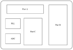
Methods and apparatus to automate a design including routing between dice
Innovation: The methods and apparatus developed to automate the design process, specifically focusing on routing between dice in semiconductor packages. this automation …
Technical Effect: The patent describes a method and apparatus for automating the design of semiconductor packages, including routing between dice. The technical efficacy of th…
Technical Problem: The technical issues addressed in this patent text are related to the increasing complexity of integrated circuitry and the need to automate the design proce…
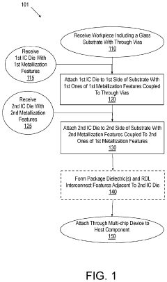
Stacked multichip IC device packages including a glass substrate
Innovation: The development of stacked multichip ic device packages that include a glass substrate. this novel approach addresses the limitations of traditional monolith…
Technical Effect: The patent scheme described in the background technology aims to improve the electrical performance of die packaging architectures. The scheme focuses on red…
Technical Problem: The patent text discusses the challenges in current IC packaging techniques, such as high cost, lower insertion efficiency, and increased z-height, and propo…
| Chiplet Packaging | View 6 First Tech |
| System in Package (SiP) | View 3 First Tech |
| Chip Scale Packaging (CSP) | View 2 First Tech |
03 Technical dynamic report in related fields
This section lists the latest updates from various fields, which will assist you to easily stay informed about the comprehensive progress of the industry and areas you might find interesting.
Internal Combustion Engine – Core Technologies
Magnetic Resonance Imaging – Typical Technologies
Ultrasound Imaging – Typical Technologies
Transmission – Technical Classification
Energy Storage Battery Management System – Core Technology