

01 Hot Tech and Product Updates
In this report, there are 2 news articles on the latest developments in the field of Semiconductor Testing – Method. These articles have been analyzed from 2 sides: the impact of technological innovations and their effects on users. From this analysis, we have summarized the following key points:
Tech Innovations
Micro-Optics Devices
China Wafer’s expertise in micro-optics devices, as mentioned in their product offerings, points to the critical role these components play in enhancing the functionality and performance of electronic devices. Micro-optics are crucial for applications requiring precise light manipulation, such as in security cameras and vehicle electronics, where high-quality imaging is essential.
Precision Measurement Technology
The news release from Optimal Engineering Systems, Inc. about their Dual-axis Yaw Pitch Stages showcases advancements in precision measurement technology. These stages are designed for sub-micron measurement of curves and angles, essential in fields like metrology, robotics, and CNC machines. The integration of high precision rotary stages and goniometers indicates a focus on enhancing the accuracy and reliability of measurements, which is critical in high-precision manufacturing and quality control processes.
Servo Motor and Encoder Technology
The use of Three-Phase Brushless Servo Motors and Quadrature Incremental Optical Encoders in the YP100-45 Series stages by OES highlights significant advancements in servo motor and encoder technology. These components ensure better repeatability, positional accuracy, and higher travel speeds, which are vital for applications requiring precise motion control, such as in automated assembly systems and inspection systems.
Wafer-Level Packaging
China Wafer Level CSP’s decision to build a plant in Malaysia highlights the strategic importance of wafer-level packaging in semiconductor manufacturing. This technology allows for the integration of more functions into smaller form factors, crucial for applications in mobile phones, security monitoring, and vehicle electronics. The investment in Malaysia, a hub with a strong electronics and automotive parts industry, suggests an alignment with technological trends favoring compact, efficient semiconductor components.
Product Effects
Global Market Reach
China Wafer Level CSP’s investment in Malaysia underscores its strategy to enhance its global market reach. By situating the plant in a strategic location known for its robust electronics manufacturing sector, the company aims to tap into the international market more effectively, leveraging local industry and talent bases to serve its predominantly overseas clientele.
Customization and Flexibility
OES’s offering of customizable Dual-axis Yaw Pitch Stages, which can be integrated into both new and existing applications, demonstrates their commitment to providing solutions that meet diverse customer needs. This flexibility is essential for catering to various industries with specific requirements, ranging from animation to aerospace, ensuring that clients receive tailored solutions that fit their unique operational demands.
Increased Production Capacity
The establishment of a new plant by China Wafer Level CSP in Malaysia is a strategic move to increase production capacity. This expansion is not only aimed at scaling up production to meet the growing demand but also at enhancing the company’s ability to serve major clients like Sony and GalaxyCore more efficiently, particularly in overseas markets.
Enhanced Precision and Accuracy
The Dual-axis Yaw Pitch Stages from OES are engineered to provide sub-micron precision in measuring curves and angles. This level of precision is crucial for industries where minute discrepancies can significantly impact the functionality and quality of the final product, such as in semiconductor manufacturing and medical devices.
Recommended News
China Wafer Jumps on Plan to Build USD50 Million Factory in Malaysia
Optimal Engineering Systems releases YP100-45 series dual-axis yaw pitch stages
02 Technologies First Made Public
In this section, you will get the latest breakthroughs in four main technical directions of Semiconductor Testing – Method. These technologies, first made public, represent the cutting-edge innovations and progress in the solar cell industry, showcasing the potential and direction of future developments.
Functional Test
| Functional Test | View 26 First Tech |
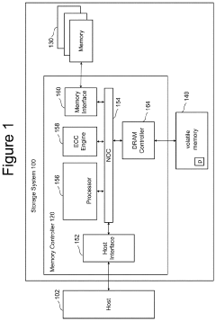
Non-volatile memory with erase depth detection and adaptive adjustment to programming
Innovation: The use of advanced detection techniques to accurately measure the erase depth in non-volatile memory. The implementation of an adaptive adjustment mechanism…
Technical Effect: The patent technology improves the reliability of data storage in non-volatile memory by enhancing the detection and adjustment of erase depth and programming.
Technical Problem: The technical problem is that users of non-volatile memory need to be able to store data reliably so that it can be read back successfully.
Automated application detection and storage savings based on intelligent workload characterization
Innovation: Automated application detection: the patent solution introduces a system and method for automatically determining the performance category of applications …
Technical Effect: The technical efficacy of the patent text is that it describes a system and method for automatically determining and executing modifications at a storage …
Technical Problem: The technical issues addressed in this patent text are related to the performance and efficiency of a storage system. The patent scheme aims to improve the …
Final Test
| Final Test | View 19 First Tech |

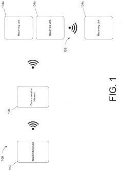
Individual building space differential pressure measurement for ventilation and air quality control
Innovation: Tubeless and wireless design: the system eliminates the need for tubes between the reference and measurement locations, reducing installation complexity and …
Technical Effect: The technical efficacy of the patent text is that it describes a tubeless and wireless self-calibrating system for accurately measuring differential pressure…
Technical Problem: The technical issues addressed in the patent text are related to the measurement and control of ventilation in buildings. The current industry standard for …
A geomagnetic differential vehicle detection method and system based on a single geomagnetic sensor
Innovation: Since the first-order difference measures the relative changes in the magnetic field at the front and back moments, this method can still accurately detect …
Technical Effect: The present invention provides a geomagnetic differential vehicle detection method based on a single geomagnetic sensor. By utilizing the first-order …
Technical Problem: Existing vehicle detection methods have the following problems: 1. When relying on environmental magnetic fields for vehicle detection, magnetic field drift …
Probe Test
| Probe Test | View 13 First Tech |
Probe card for memory chip testing
Abstract: The application discloses a probe card for memory chip testing, which includes: a base covered with an insulating film, a printed circuit board arranged on the upper surface of the base, a ceramic plate assembly arranged on the upper …
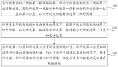
A hot spot defect detection method and equipment
Technical Effect: The invention provides a hot spot defect detection method and equipment, which determines whether the solar cell has hot spots by abutting both sides of the …
Technical Problem: Existing hot spot defect detection methods have many detection errors, resulting in low reliability of hot spot defect detection.
Visual Test
| Visual Test | View 12 First Tech |
Individual building space differential pressure measurement for ventilation and air quality control
Innovation: Tubeless and wireless design: the system eliminates the need for tubes between the reference and measurement locations, reducing installation complexity and …
Technical Effect: The technical efficacy of the patent text is that it describes a tubeless and wireless self-calibrating system for accurately measuring differential pressure…
Technical Problem: The technical issues addressed in the patent text are related to the measurement and control of ventilation in buildings. The current industry standard for …
A steady-state visual evoked potential screen flicker frequency detection device and system
Innovation: A photoelectric sensor is used to detect light changes on the screen, and the collected optical signals are converted into electrical signals and sent to the…
Technical Effect: The invention proposes a device for detecting steady-state visual evoked potential screen flicker frequency, which detects light changes on the screen …
Technical Problem: When traditional brain-computer interface equipment detects the flicker frequency of screen color blocks, there is interference from various factors such as …
| Leak Test | View 7 First Tech |
| Burn-in Test | View 2 First Tech |