

01 Hot Tech and Product Updates
In this report, there are 5 news articles on the latest developments in the field of Semiconductor Packaging – Key Modules. These articles have been analyzed from 2 sides: the impact of technological innovations and their effects on users. From this analysis, we have summarized the following key points:
Tech Innovations
Quantum Computing and Semiconductor-Based Qubits
Quantum computing represents a significant leap in processing power, capable of handling complex computations unimaginable for classical computers. This technology could transform industries by enabling new capabilities in drug discovery, financial modeling, and secure communications.
High-Speed Data Transmission
The need for high-speed data handling capabilities is critical in an era of 5G and IoT. Semiconductor packaging technologies that support faster data transmission are pivotal in enhancing user experience and device performance, impacting telecommunications and data-dependent applications like streaming and gaming.
Miniaturization and Integration
This trend is crucial as devices become more compact while consumer demand for functionality increases. Semiconductor substrates that support this trend are vital for the next generation of mobile and automotive technologies, influencing sectors from consumer electronics to transportation.
2.5D and 3D Packaging Technologies
These advanced packaging solutions address the thermal and electrical challenges of modern ICs, facilitating the development of more powerful and efficient devices. They are particularly influential in computing and network systems, where performance and energy efficiency are paramount.
Metal-Organic Chemical Vapor Deposition (MOCVD)
MOCVD technology’s ability to mass-produce quantum dot lasers economically is a game-changer for the telecommunications industry. It supports the deployment of more cost-effective and efficient optical communication systems, crucial for data center operations and internet infrastructure.
Product Effects
Increased Functionality
Devices that incorporate more functions within compact form factors are more versatile and attractive to consumers, driving sales and expanding the potential uses of technology in daily life.
Cost Reduction
Lower production costs enable manufacturers to offer more competitive pricing or invest in additional innovations, benefiting consumers and stimulating market growth.
Enhanced Computational Speed
Devices equipped with advanced semiconductor technologies deliver superior performance, meeting the demands for faster and more efficient processing in applications ranging from mobile phones to enterprise servers.
Energy Efficiency
Energy-efficient technologies not only reduce operational costs but also appeal to environmentally conscious consumers, aligning with global sustainability goals.
Scalability and Manufacturability
The ability to scale production efficiently ensures that emerging technologies can meet the growing global demand, facilitating broader adoption and standardization in the industry.
Recommended News
Global Semiconductor Package Substrates in Mobile Devices
Semiconductor-Based Qubits: Pioneering Quantum Computing with Advanced Quantum Semiconductors
Bump Pitch Transformers Will Revolutionize Advanced Packaging
Siemens introduces multiphysics cockpit for 3D IC design and verification
Researchers develop technology to mass produce quantum dot lasers for optical communications
02 Technologies First Made Public
In this section, you will get the latest breakthroughs in four main technical directions of Semiconductor Packaging – Key Modules. These technologies, first made public, represent the cutting-edge innovations and progress in the solar cell industry, showcasing the potential and direction of future developments.
Lead, Lead Frame
| Lead, Lead Frame | View 24 First Tech |
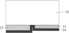
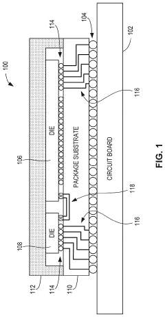
Hall Sensor Using Face Down Structure with Through Substrate Vias
Innovation: The novel design of a hall sensor using a face-down structure with through substrate vias (tsvs). this design allows for a more compact and efficient hall …
Technical Effect: The technical efficacy of this patent is the design of a semiconductor package for a Hall-effect sensor. This design allows for a more compact and efficient …
Technical Problem: The technical issue addressed in the patent text is the need to improve the size and efficiency of Hall effect sensors by utilizing a semiconductor package …
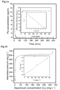
Materials and Method for Trapping Lead Leakage in Perovskite Solar Cells
Innovation: The use of a specific combination of materials for the lead trapping layer. this combination of materials has been found to be highly effective in preventing…
Technical Effect: The technical efficacy of the patent text is the development of a lead trapping layer for solar cell devices. This layer is designed to prevent lead leakage …
Technical Problem: The technical issue addressed in this patent is the potential lead leakage from perovskite solar cells, which can be harmful to the environment and human …
Packaging Structure
| Packaging Structure | View 20 First Tech |
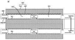
Sensing system, chip package structure, sequencing slide, and sequencing method
Innovation: The innovation of this patented solution is mainly reflected in the design of the sensing system and chip packaging structure. The sensing system adopts a …
Technical Effect: This patent text describes a sensing system, chip packaging structure, sequencing slide and sequencing method. Its technical effect is to increase sequencing…
Technical Problem: Traditional sequencing systems have shortcomings such as serious optical interference, complex lens structure, low sequencing quality, and low sequencing …
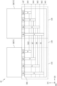
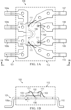
Interposer devices and semiconductor packaging structures
Innovation: The patent proposes an interposer device for passing multiple circuit signals in a semiconductor package The interposer device includes two bump areas, a …
Technical Effect: The interposer device and semiconductor packaging structure of this patent document can maintain a regular arrangement of signal lines and shielding lines …
Technical Problem: In 2.5D interposer packaging technology, how to bury through holes in the interposer device to realize the connection between signal lines of different layer…
Substrate
| Substrate | View 12 First Tech |
Innovation: The combination of a heat sink, a fan, and a coolant in a single cooling system. The use of a coolant circulated through channels in the heat sink, enhancing…
Technical Effect: The patent technology provides a cooling system for electronic devices, which can effectively dissipate heat and ensure the normal operation of the device.
Technical Problem: The technical problem is how to effectively dissipate heat from integrated circuit (IC) chips and/or semiconductor dies in electronic devices during operation.
Hall Sensor Using Face Down Structure with Through Substrate Vias
Innovation: The novel design of a hall sensor using a face-down structure with through substrate vias (tsvs). this design allows for a more compact and efficient hall …
Technical Effect: The technical efficacy of this patent is the design of a semiconductor package for a Hall-effect sensor. This design allows for a more compact and efficient …
Technical Problem: The technical issue addressed in the patent text is the need to improve the size and efficiency of Hall effect sensors by utilizing a semiconductor package …
03 Technical dynamic report in related fields
This section lists the latest updates from various fields, which will assist you to easily stay informed about the comprehensive progress of the industry and areas you might find interesting.
Ultrasound Imaging – Product Components
Transmission System – Components
Power Converter – Product Component
Electric Vehicle Motor – Design and Manufacturing
Powertrain – Product Component