

01 Hot Tech and Product Updates
In this report, there are 5 news articles on the latest developments in the field of Semiconductor Cleaning. These articles have been analyzed from 2 sides: the impact of technological innovations and their effects on users. From this analysis, we have summarized the following key points:
Tech Innovations in Semiconductor Cleaning
Van der Waals (vdW) Contacts
The research highlighted in Nature Communications introduces an all-stacking technique for fabricating 2D electrical devices. This method optimizes the interface contact between 2D materials and metal electrodes using vdW forces, which significantly enhances the electrical performance by reducing defects and improving the metal-semiconductor interface.
Silicon-Perovskite Tandem Solar Cells
LONGi Green Energy Technology’s breakthrough in achieving a 30.1% efficiency for silicon-perovskite tandem solar cells represents a significant leap in photovoltaic technology. This development not only pushes the efficiency boundaries but also underscores the commercial viability of this next-generation solar technology.
Complementary FETs (CFETs)
Imec’s development of monolithic CMOS CFET devices integrates n- and pMOS structures vertically, reducing the standard cell track heights and improving performance without degradation. This innovation is set to revolutionize logic technology, particularly in advanced semiconductor device architectures.
Graphene Field Effect Transistor (gFET)
Archer Materials has successfully fabricated gFET designs on a six-inch wafer, demonstrating the capability to produce multiple chips with consistent electronic performance. This advancement in gFET technology is crucial for applications in quantum technology and medical diagnostics, where stability and sensitivity are paramount.
Gallium Nitride (GaN) Power Products
Renesas’s acquisition and subsequent focus on GaN-based power products highlight the growing importance of wide bandgap semiconductor materials in power electronics. GaN technology offers superior performance in terms of efficiency, thermal management, and overall power handling capabilities.
Product Effects
Innovative Fabrication Techniques
The all-stacking technique for 2D devices and the advanced CFET integration process represent significant technological innovations that enhance the fabrication process, leading to better device performance and efficiency.
Enhanced Electrical Performance
Improvements in electrical performance are evident in the reduced off-state current and decreased subthreshold swing in 2D devices using vdW contacts, as well as the high on-off ratios in silicon-perovskite tandem solar cells and CFETs, which are critical for low-power and high-efficiency applications.
High Efficiency in Energy Conversion
The silicon-perovskite tandem solar cells developed by LONGi exhibit a record-breaking efficiency, highlighting the potential for high-performance energy conversion systems.
Scalability and Industrial Application
The ability to fabricate devices on a wafer-scale as demonstrated in the gFET and CFET technologies, as well as the vdW contact method, shows promise for large-scale industrial applications, making the transition from lab to market more feasible.
Stability and Consistency in Device Performance
Both the gFETs produced by Archer and the 2D devices using vdW contacts demonstrate enhanced stability and consistency, crucial for reliable application in technology and industrial sectors.
Recommended News
Archer Biochip gFET Design Fabricated on a Six-inch Wafer by Graphenea’s Foundry
Engineers integrate wafer-scale 2D materials and metal electrodes with van der Waals contacts
Imec produces first electrically functional CMOS CFET
Renesas offers GaN power transistors after Transphorm deal
02 Technologies First Made Public
In this mail, we have filtered out the latest breakthroughs in four main technical directions of Semiconductor Cleaning. These technologies, first made public, represent the cutting-edge innovations and progress in the solar cell industry, showcasing the potential and direction of future developments.
Spray Cleaning
| Spray Cleaning | View 13 First Tech |
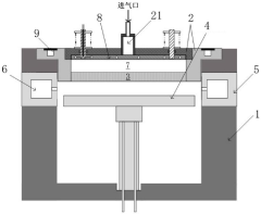
Innovation: The innovation of this patented solution is mainly reflected in the design of the sprinkler head heating device. In traditional vapor deposition equipment, …
Technical Effect: The invention provides a shower head heating device, vapor deposition equipment and a shower head temperature control method, which solves the technical …
Technical Problem: The shower head heating device solves the problems of shower head cleaning and temperature control in vapor deposition equipment.
Abstract: The present invention relates to a fluid injection device, and more specifically, to a fluid injection device for cleaning the surface of a sensor. A fluid injection device according to the present invention includes a flexible hose …
Ultrasonic Cleaning
| Ultrasonic Cleaning | View 8 First Tech |
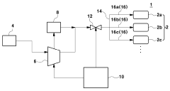
Silicon wafer grinding and cleaning device and silicon wafer grinding and cleaning method
Abstract: The invention discloses a solar silicon wafer grinding device and a silicon wafer grinding method, which include a sandblasting mechanism, an ultrasonic mechanism, an acid leaching spray mechanism, a spray rinsing mechanism and a drying …
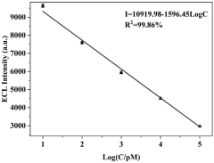
An electrochemical biosensor for detecting miR-139b and its preparation method and application
Innovation: For example, based on electrochemiluminescence technology, other advanced nanomaterials and biotechnology can be further combined to improve the performance …
Technical Effect: The present invention provides an electrochemical biosensor for detecting miR-139b. The sensor has high electrochemical luminescence response and high …
Technical Problem: Cu NCs have low quantum yield in solution and poor stability in dilute solutions, limiting their practical applications.
Plasma Cleaning
| Plasma Cleaning | View 5 First Tech |
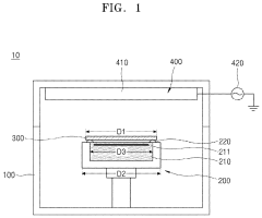
Cover wafer and method of cleaning substrate processing apparatus including the same
Abstract: A method of cleaning a substrate processing apparatus that provides a processing space for accommodating a process wafer and includes a substrate support including an internal electrode, the method includes disposing a cover wafer on an …

Innovation: By introducing periodic nanofold structures, the specific surface area of the SERS substrate can be increased, thereby enhancing the SERS effect.
Technical Effect: In the SERS substrate of the present invention, the technology of combining the template method and the surface stretch wrinkle method is used to construct …
Technical Problem: When the wrinkle structure is introduced into the existing polydimethylsiloxane (PDMS) substrate through stretch wrinkle technology, due to the regulatory …
Wet Cleaning
| Wet Cleaning | View 3 First Tech |
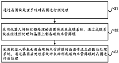
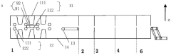
A fully automatic method and device for preparing carbon nanotube films
Innovation: The invention provides a method and device for fully automatic preparation of carbon nanotube films, which realizes fully automatic preparation of carbon …
Technical Effect: The invention provides a method and device for fully automatic preparation of carbon nanotube films, which can realize fully automatic preparation of carbon …
Technical Problem: At present, carbon nanotubes are mainly prepared through pulling method, printing method, patterning method, etc. in the existing technology. However, in the…
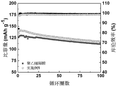
Preparation method of modified polar polyolefin porous separator and its products and applications
Innovation: By modifying the separator, the growth of lithium dendrites is inhibited, which improves the electrochemical performance and safety of the battery.
Technical Effect: The invention provides a method for preparing a modified polar polyolefin porous separator. By modifying the separator, the problem of poor affinity between …
Technical Problem: Existing lithium-ion battery separators have the following problems: 1. Poor wettability with the electrolyte, resulting in low ionic conductivity; 2. Low …
| Ozone Cleaning | View 1 First Tech |
| Dry Cleaning | View 1 First Tech |
03 Technical dynamic report in related fields
This section lists the latest updates from various fields, which will assist you to easily stay informed about the comprehensive progress of the industry and areas you might find interesting.
Wafer – Preparation Crafts
Semiconductor Deposition – Craft
Semiconductor Etching – Craft