01 Hot Tech and Product Updates
In this report, there are 5 news articles on the latest developments in the field of Wafer – Preparation Crafts. These articles have been analyzed from the effects on users of the technological innovations in this field. From this analysis, we have summarized the following key points:
Product Effects
All-Stacking Technique for 2D Electrical Devices (Nature Communications Study)
Developed a novel all-stacking technique that optimizes the interface contact between 2D materials and metal electrodes, crucial for improving the performance of 2D electrical devices. Demonstrated devices exhibited more than 95% reduction in off-state current and a 50% decrease in subthreshold swing, with a high on-off ratio. Achieved a device yield of 98.4% in wafer-scale manufacturing, showing excellent consistency and stability. Analysis: This technique addresses critical challenges in the fabrication of 2D electronic devices, offering a path towards reliable, high-performance, and scalable applications. The high yield and consistency are particularly promising for industrial applications.
Imec’s Complementary FETs (CFETs)
Introduced a novel CFET architecture with potential to reduce standard cell track heights significantly, enhancing the density and performance of integrated circuits. Demonstrated functional monolithic CMOS CFET devices with innovative process modules like MDI and stacked contacts. Analysis: Imec’s advancements in CFET technology could lead to substantial improvements in microprocessor performance and efficiency. However, the complexity of the new integration techniques and their adaptation to existing manufacturing processes pose challenges for immediate industry adoption.
Renesas’ GaN-based Power Products
Acquisition of technology for GaN-based power products aimed at meeting the demand for wide bandgap semiconductor products. Introduced devices capable of being switched using conventional silicon drivers, which could facilitate easier integration into existing systems. Analysis: While promising for specific applications in power electronics, the impact and efficacy of Renesas’ GaN products are less demonstrated in comparison to the other technologies listed. The real test will be in market adoption and performance in diverse applications.In summary, the technologies from LONGi and the all-stacking technique for 2D electrical devices stand out for their demonstrated efficacy and potential impact on their respective industries. Archer’s gFETs and Imec’s CFETs show promising advancements, though their broader industry impact remains more speculative at this stage. Renesas’ GaN-based products hold potential but require further validation in market applications.
Archer Materials (Biochip gFETs)
Successfully fabricated graphene field effect transistors (gFETs) on a six-inch wafer, a first for the company, with each chip containing 8 gFET devices. Demonstrated electronic performance and stability within expected parameters, crucial for applications in quantum technology and medical diagnostics. Analysis: While this represents a significant step forward for Archer in scaling up their gFET technology, the real-world application and mass production readiness are yet to be fully demonstrated compared to the more established technologies like those from LONGi and the 2D electrical device team.
Recommended News
Archer Biochip gFET Design Fabricated on a Six-inch Wafer by Graphenea’s Foundry
Engineers integrate wafer-scale 2D materials and metal electrodes with van der Waals contacts
Imec produces first electrically functional CMOS CFET
Renesas offers GaN power transistors after Transphorm deal
02 Technologies First Made Public
In this mail, we have filtered out the latest breakthroughs in four main technical directions of Wafer – Preparation Crafts. These technologies, first made public, represent the cutting-edge innovations and progress in the solar cell industry, showcasing the potential and direction of future developments.
Wafer Lapping, Grinding, Polishing
| Wafer Lapping, Grinding, Polishing | View 42 First Tech |
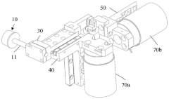
A connection component for a turret-type crystal bonding device
Abstract: The invention discloses a connection assembly for a turret-type die-bonding device. The connection assembly includes a third connection unit (50) and a base plate (60); the base plate (60) is fixedly arranged relative to the ground and …
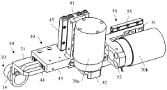
Connection structure unit for turret type die bonding device
Innovation: This patent provides a connection structural unit for a turret-type die-bonding device. This connection structure unit can realize the connection between …
Technical Effect: The connection structural unit provided by the invention can realize the connection between the voice coil motor and the bonding head, so that the voice …
Technical Problem: In a turret-type die-bonding device, how to design and improve the connection component between the second motor and the bonding head so that the second …
Wafer Cutting, Dicing, Slicing
| Wafer Cutting, Dicing, Slicing | View 28 First Tech |
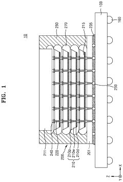
Semiconductor chip, semiconductor package, and wafer dicing method
Innovation: Technical problem:the technical issues addressed in this patent text are related to the manufacturing process of semiconductor devices. specifically, the …
Technical Effect: The technical efficacy of the patent scheme is to increase the yield of semiconductor devices by providing a semiconductor chip, a semiconductor package, and…
Technical Problem: The patent text discusses a semiconductor chip, semiconductor package, and wafer dicing method that aim to increase the yield of semiconductor devices by …
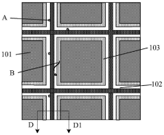
Semiconductor structure and formation method thereof, chip formation method
Innovation: By forming grooves in the dicing lane area and filling them with buffer layer materials, damage to the wafer structure during the cutting process can be …
Technical Effect: The invention provides a method for forming a semiconductor structure. By forming grooves in the dicing track area of the wafer and forming a buffer layer …
Technical Problem: Existing wafer cutting methods have certain limitations, which will have a certain impact on product performance or yield.
Wafer Inspection
| Wafer Inspection | View 25 First Tech |
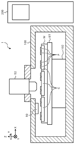
Inspection device and inspection method
Abstract: Provided are an inspection device and an inspection method capable of performing a visual inspection of a wafer accurately and at high speed. An inspection device (1, 1A, 1B) comprises: a camera (50) that captures an image of an object …
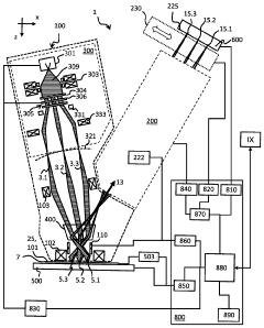
Multi-beam charged particle microscope design with detection system for fast charge compensation
Innovation: The use of a multi-aperture plate to generate a bundle of primary charged particle beamlets. The parallel scanning of an object to be inspected with a …
Technical Effect: The patent describes a multi-beam charged particle microscope that improves imaging contrast. It also includes a method for inspecting semiconductor features…
Technical Problem: The technical issues addressed in this patent text are related to the improvement of imaging contrast in a multi-beam charged particle microscope, as well as…
Wafer Stacking
| Wafer Stacking | View 6 First Tech |
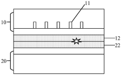
Wafer bonding structure and stacked back-illuminated image sensor, and formation method
Innovation: By introducing a metal shielding layer in the dicing lane area of the first wafer, the first metal layer and the second metal layer can be effectively …
Technical Effect: The technical effect of this patent text is to provide a wafer bonding structure and formation method that can increase the process window causing bonding …
Technical Problem: After the wafers are bonded, when processing the back of the top wafer, due to the different optical properties of the metal and dielectric at the bonding …
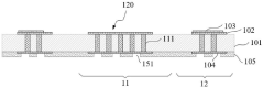
A Ka-band transceiver component and its preparation method
Innovation: It adopts the design of chip stack and RF connector. By stacking multiple chip units together, the integration of components can be improved and the size of…
Technical Effect: The invention provides a Ka-band transceiver component, which achieves high performance, low cost and miniaturization through the design of a chip stack and …
Technical Problem: Existing transceiver components have problems such as low integration and large size.
| Wafer Orientation | View 2 First Tech |
| Wafer Chamfering | View 1 First Tech |
03 Technical dynamic report in related fields
This section lists the latest updates from various fields, which will assist you to easily stay informed about the comprehensive progress of the industry and areas you might find interesting.
Semiconductor Cleaning
Semiconductor Deposition – Craft
Semiconductor Etching – Craft