
Introduction
This article outlines the key steps in semiconductor manufacturing, providing a detailed and expert-level breakdown of each stage. We’ll walk through the complexities and innovations involved, offering insights for a comprehensive understanding.
Step 1: Wafer Preparation and Cleaning
The process begins with producing high-purity silicon. The Czochralski method grows silicon into single-crystal ingots. These ingots are sliced into thin wafers and polished for a smooth, defect-free surface. Chemical-mechanical polishing (CMP) removes any remaining imperfections, ensuring the wafer is ready for further steps.
Step 2: Oxidation
During oxidation, a thin silicon dioxide layer forms on the wafer’s surface. This insulating layer protects the wafer throughout the remaining processing steps. A uniform and high-quality oxide layer is essential to the device’s overall performance. Even minor imperfections in this layer can impact functionality and efficiency.
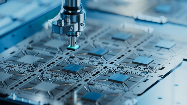
Step 3: Photolithography
Photolithography transfers detailed circuit patterns onto the wafer. First, a photoresist material coats the wafer. Ultraviolet light exposes the wafer through a mask with the desired pattern. The light hardens the photoresist, while developers remove the unexposed parts, revealing the silicon dioxide layer beneath.
Step 4: Etching
Etching removes exposed silicon dioxide and other materials to create precise circuit patterns. Wet chemical or dry plasma etching techniques are applied. Accuracy in etching is crucial for defining fine features. This precision ensures that each semiconductor component operates as designed.

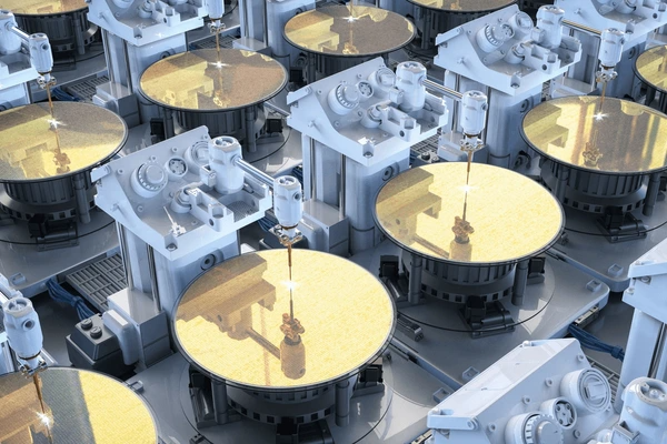
Step 5: Thin Film Deposition
Thin films of materials like silicon nitride, polysilicon, and metals are deposited onto the wafer. Techniques such as chemical vapor deposition (CVD), physical vapor deposition (PVD), and atomic layer deposition (ALD) control film thickness and properties. These layers are essential for the device’s functionality.
Step 6: Ion Implantation
Ion implantation modifies the silicon wafer’s electrical properties by introducing dopants. High-energy ions accelerate and implant into the wafer, forming n-type or p-type regions. This step creates the active regions in transistors and other devices. It ensures the wafer has the correct conductivity for operation.
Step 7: Metallization
Metallization deposits metal layers to establish electrical connections between components. Aluminum or copper is commonly used for interconnects. Photolithography and etching define these interconnect structures. This process ensures efficient electrical paths between all components.
Step 8: Electrical Testing
After processing, devices undergo electrical testing. Electrical signals probe the devices to verify their functionality. Defective units are discarded, ensuring only functional devices proceed to the next phase.
Step 9: Packaging
Packaging protects semiconductor devices and prepares them for integration into systems. Devices are cut from the wafer, mounted on lead frames or substrates, and encapsulated in protective materials. Advanced methods like flip-chip and wafer-level packaging improve performance while reducing size.
Conclusion: The Future of Semiconductor Manufacturing
Technological Innovations
- Scaling Challenges and Solutions: As devices shrink below 100 nm, new issues like line edge roughness and reliability emerge. Advanced techniques and materials, such as SiC and GaN, address these challenges.
- Data-Driven Manufacturing: Data-driven methods, like statistical process control (SPC) and data mining, are key to improving stability and yield. These tools enable real-time monitoring and proactive decision-making, boosting productivity and reducing cycle times.
- 3D Packaging and Fusion Technologies: 3D packaging and fusion technologies, like OneDRAM and OneNAND, address the limits of traditional planar designs. These innovations provide higher integration densities and improved performance for next-gen applications.
Market and Business Model Transformations
- Geographical Redistribution: The semiconductor industry will see manufacturing centers shift to regions with favorable economic and political conditions. This change will impact the global supply chain and the roles of industry leaders.
- Fablite and Fabless Models: The high cost of state-of-the-art fabrication facilities is pushing companies to adopt fablite or fabless models. This shift encourages collaboration between design and manufacturing entities, optimizing resources and reducing time-to-market.
- Industry Consolidation: The industry is consolidating as companies merge to pool resources and expertise. This trend helps manage rising R&D costs and stay competitive in a market of low chip prices and rapid advancements.
Sustainable Manufacturing Practices
- Clean Energy Integration: Photovoltaic (PV) systems and large-scale PV module manufacturing play a crucial role in the clean energy economy. Semiconductor technologies, especially those using wide band gap materials, enable efficient DC power generation.
- Environmental Impact Reduction: Reducing the environmental footprint of semiconductor manufacturing includes developing processes that lower waste and energy use. For example, improved vacuum leak detection enhances yield and minimizes rework.
Future Research and Development Directions
- Advanced Materials and Processes: Research into new materials and fabrication processes will push the boundaries of semiconductor performance. This includes exploring alternative substrates, innovative deposition techniques, and advanced lithography methods.
- Collaborative R&D Efforts: Joint programs between companies, research institutions, and government agencies are crucial for tackling the challenges of next-gen semiconductor technologies. These collaborations speed up breakthroughs and ensure the industry’s long-term growth.
To get detailed scientific explanations of Semiconductor Manufacturing, try Patsnap Eureka.
