Indium Tin Oxide (ITO) is one of the most widely used materials in modern electronic and optoelectronic industries. Its unique ability to combine high electrical conductivity with excellent optical transparency has made it a fundamental component in many everyday technologies, including touch screens, LCD displays, solar panels, and smart windows. However, while ITO is a highly valuable material, it also presents several technical and economic challenges that continue to drive global research toward better alternatives.
This article explains what ITO material is, explores its structure and properties, highlights its major benefits in technology, and examines the challenges it faces in future applications.
What Is ITO Material?
Curious about the structure or real-world applications of ITO material? Eureka Technical Q&A connects you with materials science experts who can explain its unique properties, benefits in electronics, and challenges in manufacturing—helping you better understand how indium tin oxide is shaping modern technology and innovation.
Indium Tin Oxide (ITO) is a mixed oxide ceramic composed mainly of indium oxide (In₂O₃) and tin oxide (SnO₂). The typical ratio used in ITO films is approximately 90% indium oxide to 10% tin oxide by weight. This material belongs to a class of transparent conductive oxides (TCOs), meaning it can transmit visible light while conducting electricity — a rare and valuable property combination.
In practical use, ITO is typically applied as a thin film coating on glass, plastic, or other surfaces using techniques such as sputtering, evaporation, or chemical vapor deposition. These films are incredibly thin, usually ranging from 10 nm to 200 nm in thickness, allowing for both transparency and conductivity in various electronic devices.
Structure and Properties of ITO Material
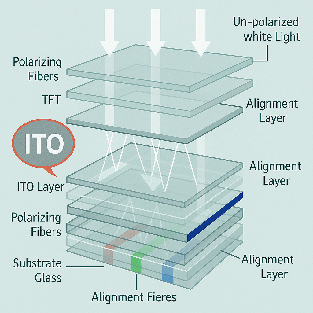
At the atomic level, Indium Tin Oxide has a cubic crystal structure, inherited mainly from indium oxide’s bixbyite phase. The inclusion of tin atoms into the indium oxide lattice results in additional free electrons. These free electrons are responsible for the electrical conductivity of ITO.
The dual-functionality of Indium Tin Oxide — as a transparent material and a conductor — arises from its wide bandgap and the presence of free carriers within its structure. The wide bandgap (over 3 eV) prevents absorption of visible light, maintaining transparency, while the extra electrons provided by tin doping enable electrical conduction.
Key Properties of ITO:
- High optical transparency in the visible light range (400–700 nm)
- Electrical conductivity comparable to metals in thin-film form
- Reflectivity in infrared regions
- Adjustable transparency and conductivity based on film thickness and processing conditions
- Wide bandgap semiconductor behavior
Benefits of ITO in Modern Technology
The widespread use of ITO is primarily due to its ability to perform as both a transparent material and a conductor — a rare feature that makes it invaluable for the production of touch-sensitive screens, energy devices, and display technologies.
Optical Transparency with Electrical Conductivity
Indium Tin Oxide allows visible light to pass through while providing excellent electrical conductivity. This balance is essential for touch panels, smartphone screens, interactive displays, and solar cells, where both clarity and functionality are required.
Compatibility with Thin-Film Manufacturing
ITO films can be deposited using standard industrial methods such as sputtering, which makes integration into existing manufacturing processes straightforward and cost-effective at scale.
Tunability of Properties
Manufacturers can adjust the conductivity and transparency of Indium Tin Oxide films by modifying factors like doping levels, film thickness, and deposition conditions. This tunability offers versatility for various design needs.
Wide Range of Applications
ITO’s unique characteristics have led to its integration in a broad range of technologies, including:
- Touchscreen panels
- LCD and OLED displays
- Solar cells and photovoltaic devices
- Smart glass and smart windows
- Transparent antennas
- LED lighting systems
- Flexible electronics (to a limited extent)
Application Cases
| Product/Project | Technical Outcomes | Application Scenarios |
|---|---|---|
| ITO Thin Films Samsung Electronics Co., Ltd. | Achieves high near-IR transparency and excellent conductivity through low-energy sputter deposition process. | Photovoltaic devices requiring both high transparency and conductivity. |
| ITO Nanowires The Boeing Co. | Enhances electrical conductivity of nanowires through electrospinning and heat treatment with specific molar ratios. | Advanced applications requiring high-conductivity nanoscale materials. |
| Nano-scale ITO Powders Evonik Operations GmbH | Produces high conductivity and transparency ITO powders with reduced indium content through controlled synthesis. | Various applications requiring cost-effective, high-performance TCO materials. |
| ITO Particles FUJIFILM Corp. | Efficiently produces ITO particles with stable near-infrared absorption and low Abbe numbers through optimized synthesis process. | Optical materials requiring specific light absorption and refractive properties. |
| ITO Coatings Ming Chi University of Technology | Enables cost-effective and efficient large-scale production of high-quality ITO coatings for complex shapes through electroplating and annealing. | Applications requiring ITO coatings on complex-shaped surfaces. |
Technological Challenges and Limitations of ITO
Despite its advantages, ITO also comes with significant drawbacks that limit its use in certain next-generation applications. These challenges have created growing interest in finding alternative materials that can offer similar or superior performance.
High Cost of Indium
One of the primary challenges with Indium Tin Oxide is the scarcity and expense of indium. Indium is a rare metal primarily sourced as a byproduct of zinc mining, and its limited availability makes the price of Indium Tin Oxide susceptible to market fluctuations.
Brittleness of ITO Films
ITO is inherently brittle, especially when applied as a thin film. This brittleness makes it prone to cracking under mechanical stress, limiting its use in flexible displays or foldable electronic devices.
Limited Flexibility
As industries move toward wearable electronics and flexible displays, ITO’s inability to bend or stretch without damage poses a significant technological limitation.
Environmental and Supply Risks
Mining and refining indium raise environmental concerns, while its concentrated supply in specific regions poses a geopolitical risk for industries dependent on Indium Tin Oxide.
Processing and Temperature Constraints
ITO films often require high-temperature processing to achieve optimal conductivity and transparency, restricting their application to temperature-resistant substrates like glass and limiting their use on flexible plastics.
Future of ITO and Alternative Materials
Due to these limitations, there is a strong research push toward developing alternative transparent conductive materials that could complement or even replace ITO in certain applications.
Promising ITO Alternatives Include:
- Graphene: Extremely strong and flexible, but expensive to produce at scale.
- Silver Nanowires: Highly conductive and flexible, but suffer from surface roughness and oxidation.
- Carbon Nanotubes: Flexible with good conductivity, but challenges remain in uniform film formation.
- Conductive Polymers: Low-cost and flexible but lower conductivity compared to ITO.
- Metal Mesh Films: Offering both flexibility and conductivity but visible patterns can reduce transparency.
While none of these materials currently offer a perfect replacement for Indium Tin Oxide across all applications, hybrid approaches and material engineering may allow industries to overcome ITO’s limitations in specific use cases.
Conclusion
Indium Tin Oxide (ITO) has been a vital material in the development of modern display and optoelectronic technologies. Its rare combination of transparency and electrical conductivity has enabled the rise of touchscreens, high-resolution displays, solar panels, and smart windows.
However, challenges related to cost, brittleness, and supply constraints have spurred global research efforts into alternative materials. While Indium Tin Oxide continues to dominate in many industrial applications, the future of transparent conductors may soon expand to include new, more flexible, and sustainable materials.
The evolution of display technology, wearable electronics, and renewable energy solutions will likely depend on the successful advancement of ITO alternatives or next-generation hybrid materials that overcome its current challenges.
FAQs
ITO is composed of about 90% indium oxide (In₂O₃) and 10% tin oxide (SnO₂).
The wide bandgap of indium oxide ensures transparency, while tin doping introduces free electrons, enabling electrical conductivity.
Indium Tin Oxide is widely used in touchscreen panels, displays, solar cells, smart windows, LEDs, and transparent electronics.
High cost, brittleness, limited flexibility, environmental concerns, and dependence on rare indium resources.
Yes, alternatives like graphene, silver nanowires, carbon nanotubes, and conductive polymers are under active development for flexible and cost-sensitive applications.
To get detailed scientific explanations of Indium Tin Oxide, try Patsnap Eureka.