According to IDC’s Worldwide Semiconductor Supply Chain Tracking Intelligence latest report, the global semiconductor market, following a recovery in 2024, is expected to experience steady growth in 2025. The broadly defined Foundry 2.0 market— encompassing foundry, non-memory IDM, OSAT, and photomask making—is projected to reach a market size of $298 billion in 2025, with year-over-year growth of 11%, signaling a transition from a recovery phase in 2024 to a growth phase in 2025. Over the long term, the compound annual growth rate (CAGR) from 2024 to 2029 is projected to reach 10%. This growth is catalyzed by the continuous rise in AI demand and a gradual recovery in non-AI demand.
The global production timeline for 2nm semiconductor process nodes in 2025
1.TSMC (Taiwan Semiconductor Manufacturing Company) – N2 Process
·Mass Production Timeline: TSMC plans to begin mass production of its 2nm (N2) process by the end of 2025. It has already secured orders for Apple’s A20 chips, expected to power the iPhone 18 Pro series.
·Technical Highlights: N2 will be the world’s first node to adopt gate-all-around (GAA) nanosheet transistors, delivering a 15% performance improvement and 30% power reduction. It supports integration of up to 12 stacks of HBM4 on a 100×100 mm package substrate.
2.Samsung – SF2 Series
·Mass Production Timeline: Samsung is targeting mass production of its 2nm GAA (gate-all-around) process in 2025.
·Technical Highlights: Utilizing GAA transistor architecture, it achieves a transistor density of 333 million per mm². Multiple variants are being introduced for different applications: SF2P for mobile, SF2X/SF2Z for AI computing, and SF2A for automotive. The SF2Z version incorporates backside power delivery (BSPDN), improving signal transmission efficiency by 20%.
3.Intel – 18A Process
·Mass Production Timeline: Intel’s 18A process technology is on track for high-volume production in the second half of 2025.
·Technical Highlights: With an effective node size of 1.8nm, it features RibbonFET (GAA architecture) and PowerVia backside power delivery. Gate length is reduced to 6nm, with silicon layer thickness as low as 1.7nm.
4.Rapidus (Japan) – 2nm GAA
·Mass Production Timeline: Rapidus began trial production of its 2nm GAA process in July 2025, with full-scale mass production planned for 2027.
·Technical Highlights:
a.Leapfrogs from 40nm directly to 2nm by leveraging IBM’s GAA technology and EUV lithography support from IMEC.
b.Employs a monolithic wafer processing strategy combined with AI-driven yield optimization.
c.Focuses on application-specific markets such as AI and autonomous driving, strategically avoiding direct competition with TSMC.
Latest breakthroughs in semiconductor HBM4 memory technology in 2025
·SK hynix:
Began shipping 12‑layer HBM4 samples in Q1 2025, the first globally. These deliver over 2 TB/s bandwidth per stack (≈60% faster than HBM3E) with a 36 GB capacity via advanced MR‑MUF packaging. Mass production is targeted for H2 2025.
·Micron:
Started shipping 36 GB 12‑high HBM4 samples built on its 1‑β DRAM process in mid‑2025. Offers speeds over 2 TB/s per stack and 20% better power efficiency versus HBM3E. Full-scale production expected in early 2026.
·Samsung:
Fast‑tracking HBM4 development; trial production underway, aiming for mass production by late‑2025. Plans include eight‑ to sixteen‑die stacks using hybrid bonding.
·JEDEC Standardization:
JESD270‑4 HBM4 standard formally released in April 2025, specifying a 2048‑bit interface, support for up to 16‑die stacks (64 GB), and target data rates of 8 Gb/s per pin (≈2 TB/s).
Latest advancements in high-density packaging and heterogeneous integration in semiconductors in 2025
1. High-Density Packaging & HBM4 Support
·Hanmi Semiconductor has introduced the TC BONDER 4, a dedicated bonding tool tailored for HBM4 production. It enables stacking up to 16 layers, raising DRAM per‑stack capacity from 24 Gb to 32 Gb, boosting speed by 60% while cutting power to 70% of HBM3E levels.
·TSMC CoWoS: In 2025, TSMC's CoWoS (Chip-on-Wafer-on-Substrate) packaging capacity will double to 660,000 wafers. It integrates liquid-cooled microchannel technology, achieving a power density of 2.5 W/mm²—three times that of traditional air cooling. The platform supports 12 HBM4 stacks with 6.4 GT/s bandwidth, effectively addressing thermal bottlenecks in AI chips.
·Intel SLT Technology: Intel's Selective Layer Transfer (SLT) packaging boosts throughput by 100× and enables hybrid bonding of ultra-thin dies, offering a flexible architecture optimized for AI processors.
·JCET XDFOI™: JCET’s XDFOI™ 2.5D packaging—covered by Chinese patent CN222421962U—enhances thermal dissipation efficiency by 20%, advancing high-performance AI packaging solutions.
·Industry players including Samsung, and SK Hynix are rapidly scaling CoWoS and 2.5D/3D IC platforms to match rising AI-driven HBM4 demand, doubling packaging volumes by 2025.
2. Co‑Packaged Optics (CPO) & Photonic Integration
·TSMC to Validate 1.6T Optical Engine in 2025: TSMC will validate its 1.6 Tbps optical engine in 2025, leveraging SoIC-X chip stacking technology. This approach is expected to reduce optical module costs by 40% and address the "memory wall" bottleneck in AI servers by significantly enhancing data bandwidth and integration efficiency.
Materials and Device Innovation: The Rise of Fourth-Generation Semiconductors
1.Wide Bandgap Material Industrialization:
·Silicon Carbide (SiC): Accelerated transition to 8-inch substrate capacity (ST, ROHM, United Nova Technology to commence mass production in 2025), with costs reduced by 30%.
·Gallium Oxide (Ga₂O₃): FLOSFIA (Japan) to start mass production in 2025; breakdown field strength is three times that of SiC, with costs only one-fifth of silicon-based substrates.
·Two-Dimensional Materials: Intel developing 2D GAA transistors (gate length of 30 nm); molybdenum disulfide (MoS₂)-based processors reduce power consumption by 90%.
2.Interconnect Technology Revolution:
·Subtractive Ruthenium Interconnects: Intel replacing copper interconnects; air-gap technology reduces line-to-line capacitance by 25%, addressing resistivity surge challenges below 2 nm nodes.
AI-Driven Design and Manufacturing Revolution
1.AI-EDA Integration:
·Synopsys, Inc. and NVIDIA launch an AI design platform, shortening verification cycles by 50% with yield prediction errors under 1%.
·Empyrean Technology patents up 36.1% in 2024, achieving breakthroughs in 3 nm physical verification algorithms.
2.Smart Manufacturing and Predictive Maintenance:
·TSMC’s 2 nm production lines achieve 99.9% defect detection accuracy via AI machine vision, reducing downtime by 30%.
·Aitomatic’s open-source large model SemiKong improves first-tapeout yield rates.
Future Technology High Grounds and Challenges
Quantum Computing Industrialization: IBM plans to launch its 1,386-qubit Kookaburra processor in 2025; China’s Zuchongzhi 3.0 (105-qubit) processor has achieved breakthroughs in quantum error correction.
RISC-V Ecosystem Expansion: By 2025, global shipments of RISC-V cores are expected to reach 80 billion; Alibaba’s Xuantie C930 server CPU has entered mass production, challenging the Arm ecosystem.
Lithography Technology Localization: While ASML dominates EUV lithography, China is advancing via DUV multiple patterning (SMIC’s 5nm yield at 35%) and securing patents for SSMB-EUV light sources, opening alternative paths.
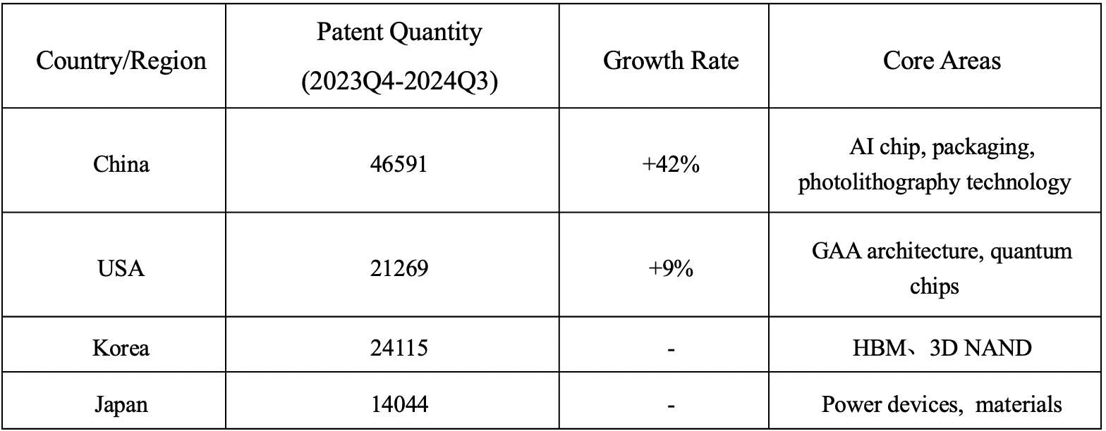
Global Semiconductor Competition—The “Tri-Polar” Landscape:
·United States: Leads in GAA architecture and AI chip design (highest patent quality density).
·East Asia: Taiwan and South Korea lead in advanced nodes and memory (TSMC 2nm, SK Hynix HBM4); China is rapidly increasing patent filings and packaging innovations.
·Europe: Focused on automotive-grade semiconductors (Infineon holds 40% market share in SiC).
Future Directions:
·Material substitution (e.g., gallium oxide, 2D materials) to reduce reliance on silicon.
·Chiplet-based heterogeneous integration to bypass process node limitations (already applied in Horizon Robotics’ J6).
·AI–manufacturing integration to shorten R&D cycles (e.g., TSMC’s cuLitho computational lithography platform).
Infuse Insights into Chip R&D with PatSnap Eureka
Whether you're exploring novel transistor architectures, monitoring global IP filings in advanced packaging, or optimizing your semiconductor innovation roadmap—Patsnap Eureka empowers you with AI-driven insights tailored to the pace and complexity of modern chip development.
Patsnap Eureka, our intelligent AI assistant built for R&D professionals in high-tech sectors, empowers you with real-time expert-level analysis, technology roadmap exploration, and strategic mapping of core patents—all within a seamless, user-friendly interface.
👉 Join the new era of semiconductor R&D. Try Patsnap Eureka today and experience the future of innovation intelligence.