

Achieve Optimal VLSI Chip Yield Using DFM Techniques
MAR 7, 20269 MIN READ
Generate Your Research Report Instantly with AI Agent
Patsnap Eureka helps you evaluate technical feasibility & market potential.
VLSI DFM Background and Yield Optimization Goals
Very Large Scale Integration (VLSI) technology has evolved dramatically since its inception in the 1970s, transforming from simple integrated circuits to complex systems-on-chip containing billions of transistors. The continuous scaling of semiconductor devices, following Moore's Law, has enabled unprecedented computational capabilities while simultaneously introducing significant manufacturing challenges that directly impact chip yield.
Design for Manufacturing (DFM) emerged as a critical discipline in the 1990s when traditional design approaches began encountering systematic yield limitations. As feature sizes shrunk below 180nm, manufacturing variability became increasingly problematic, necessitating a paradigm shift from post-design manufacturing optimization to manufacturing-aware design methodologies. DFM represents the integration of manufacturing knowledge into the design process, ensuring that circuit layouts are inherently manufacturable and robust against process variations.
The evolution of DFM techniques has been driven by the relentless pursuit of higher transistor density and improved performance. Early DFM focused primarily on design rule compliance and basic lithographic considerations. However, as technology nodes advanced to 65nm, 45nm, and beyond, DFM expanded to encompass comprehensive process variation modeling, advanced lithography effects, and systematic defect mitigation strategies.
Contemporary VLSI manufacturing faces unprecedented challenges including extreme ultraviolet lithography complexities, multi-patterning requirements, and three-dimensional device architectures. These technological advances demand sophisticated DFM approaches that address not only traditional yield detractors but also emerging failure mechanisms such as stress-induced defects, electromigration in narrow interconnects, and quantum effects in ultra-scaled devices.
The primary objective of implementing DFM techniques in VLSI design is to achieve optimal chip yield through proactive manufacturing consideration during the design phase. This encompasses minimizing systematic yield loss through layout optimization, reducing random defect susceptibility via redundancy and spacing strategies, and ensuring process robustness across manufacturing variations. Additionally, DFM aims to accelerate time-to-market by reducing design-manufacturing iterations and enabling first-silicon success rates.
Modern yield optimization goals extend beyond traditional parametric and functional yield metrics to include reliability, power efficiency, and performance consistency across process corners. The ultimate target is achieving economically viable manufacturing yields while maintaining competitive performance characteristics and meeting stringent reliability requirements for diverse application domains ranging from consumer electronics to automotive and aerospace systems.
Market Demand for High-Yield VLSI Manufacturing
The global semiconductor industry faces unprecedented pressure to maximize manufacturing yields as chip complexity continues to escalate and production costs soar. Advanced process nodes below 10nm present significant manufacturing challenges, where even minor defects can render entire wafers unusable. This economic reality has created substantial market demand for sophisticated Design for Manufacturing techniques that can optimize VLSI chip yield from the earliest design stages.
Market drivers stem from multiple converging factors. The proliferation of artificial intelligence, 5G communications, and Internet of Things applications demands high-performance semiconductors with stringent quality requirements. Automotive electronics, particularly for autonomous vehicles, require near-zero defect rates, making yield optimization critical for market viability. Consumer electronics manufacturers face intense price competition, making manufacturing efficiency a key differentiator.
The financial implications of yield optimization are substantial. Leading-edge fabrication facilities represent investments exceeding tens of billions of dollars, making every percentage point of yield improvement economically significant. Poor yields directly translate to higher per-unit costs, reduced profit margins, and potential supply chain disruptions. Companies that achieve superior yields gain competitive advantages through lower production costs and more reliable product delivery.
Foundry services represent a particularly dynamic market segment driving DFM adoption. Major foundries compete intensively on yield performance, offering comprehensive DFM rule sets and optimization services to attract customers. This competition has accelerated the development of advanced DFM methodologies and tools, creating a robust ecosystem of specialized software vendors and consulting services.
Emerging applications in quantum computing, neuromorphic processors, and advanced sensor technologies present new yield challenges that traditional manufacturing approaches cannot adequately address. These specialized markets demand innovative DFM solutions tailored to unique device architectures and performance requirements.
The market demand extends beyond traditional semiconductor companies to include system integrators, electronic design automation tool vendors, and manufacturing equipment suppliers. This broad ecosystem reflects the comprehensive nature of yield optimization challenges and the substantial economic opportunities for companies that can deliver effective DFM solutions across the entire semiconductor value chain.
Current DFM Implementation Status and Yield Challenges
The current implementation of Design for Manufacturing (DFM) techniques in VLSI chip production presents a complex landscape of varying adoption levels and persistent yield challenges across the semiconductor industry. While leading foundries have integrated sophisticated DFM methodologies into their design flows, the implementation depth and effectiveness vary significantly between different technology nodes and manufacturing facilities.
Advanced semiconductor manufacturers have deployed comprehensive DFM rule sets that encompass lithography-aware design rules, chemical mechanical polishing (CMP) optimization guidelines, and metal fill insertion strategies. These implementations typically achieve yield improvements of 15-25% compared to traditional design approaches. However, the complexity of modern process technologies, particularly at 7nm and below, has introduced new categories of yield detractors that existing DFM solutions struggle to address effectively.
Lithographic yield challenges remain the most significant obstacle in current DFM implementations. Despite extensive use of optical proximity correction (OPC) and resolution enhancement techniques (RET), pattern fidelity issues continue to impact yield, especially for critical dimension uniformity and overlay accuracy. The transition to extreme ultraviolet (EUV) lithography has introduced additional complexities, including stochastic effects and mask defectivity concerns that current DFM methodologies inadequately address.
Manufacturing variability represents another critical challenge area where current DFM implementations show limitations. Process variations in parameters such as gate length, threshold voltage, and interconnect resistance create systematic yield losses that traditional corner-based design approaches cannot fully mitigate. The increasing impact of random dopant fluctuations and line edge roughness at advanced nodes further compounds these challenges.
Thermal and mechanical stress-induced failures have emerged as significant yield detractors that existing DFM frameworks inadequately address. Current implementations often lack comprehensive stress-aware design rules, leading to reliability issues that manifest as early-life failures or reduced operational lifetimes. The integration of through-silicon vias (TSVs) in 3D integrated circuits has introduced additional mechanical stress considerations that conventional DFM approaches do not sufficiently cover.
Design rule checking (DRC) and layout versus schematic (LVS) verification tools, while sophisticated, still exhibit gaps in capturing complex manufacturing interactions. Multi-patterning decomposition conflicts, particularly in self-aligned double patterning (SADP) and self-aligned quadruple patterning (SAQP) processes, frequently escape current DFM verification flows, resulting in manufacturing failures discovered only during production.
The economic impact of these yield challenges is substantial, with industry estimates suggesting that inadequate DFM implementation can result in 20-40% yield loss for complex system-on-chip designs at advanced nodes. This translates to significant revenue impact and extended time-to-market for new products, highlighting the urgent need for more comprehensive and effective DFM solutions.
Existing DFM Solutions for Yield Enhancement
01 Defect detection and testing methods for yield improvement
Various testing and inspection techniques are employed during VLSI chip manufacturing to detect defects early in the production process. These methods include electrical testing, optical inspection, and automated defect classification systems that identify problematic areas on wafers. By implementing comprehensive testing protocols at multiple stages of fabrication, manufacturers can identify yield-limiting defects and take corrective actions to improve overall chip yield.- Defect detection and testing methods for yield improvement: Various testing and inspection techniques are employed to detect defects in VLSI chips during manufacturing. These methods include electrical testing, optical inspection, and automated defect classification systems that identify faulty chips early in the production process. By implementing comprehensive testing protocols at multiple stages of fabrication, manufacturers can isolate defective units and improve overall chip yield through better quality control and process monitoring.
- Redundancy and repair techniques for functional yield enhancement: Redundancy schemes incorporate spare circuit elements such as memory cells, rows, columns, or functional blocks that can replace defective components identified during testing. Laser repair, fuse programming, and other reconfiguration methods enable defective chips to be salvaged by activating redundant elements. These techniques significantly increase functional yield by allowing chips with minor defects to be repaired and sold rather than discarded.
- Process optimization and statistical process control: Manufacturing yield is improved through careful optimization of fabrication processes including lithography, etching, deposition, and doping steps. Statistical process control methods monitor critical parameters and identify process variations that affect yield. By analyzing yield data and correlating it with process parameters, manufacturers can adjust processing conditions to minimize defects and maximize the number of functional chips per wafer.
- Design for manufacturability and yield-aware design: Chip designs are optimized to improve manufacturability by considering fabrication constraints and common defect mechanisms. This includes techniques such as design rule checking, critical area analysis, and layout modifications that reduce sensitivity to manufacturing variations. Yield-aware design methodologies incorporate statistical models of defects and process variations during the design phase, enabling designers to create layouts that are more robust to manufacturing imperfections.
- Wafer-level and die-level yield modeling and prediction: Mathematical models and simulation tools are used to predict and analyze chip yield based on defect density, critical area, and other manufacturing parameters. These models help identify yield-limiting factors and guide improvement efforts. Yield prediction techniques enable manufacturers to estimate production outcomes, optimize manufacturing strategies, and make informed decisions about process changes before committing to full-scale production.
02 Redundancy and fault-tolerant design techniques
Incorporating redundant circuits and fault-tolerant architectures into chip designs allows defective components to be bypassed or replaced with functional alternatives. This approach includes spare rows and columns in memory arrays, redundant logic blocks, and programmable interconnects that can be reconfigured to avoid defective areas. These design strategies significantly increase the probability that chips with minor defects can still function properly, thereby improving manufacturing yield.Expand Specific Solutions03 Process control and optimization methods
Advanced process control techniques monitor and adjust manufacturing parameters in real-time to maintain optimal conditions throughout fabrication. Statistical process control, feedback mechanisms, and adaptive algorithms help minimize process variations that lead to defects. By maintaining tight control over critical parameters such as temperature, pressure, chemical concentrations, and exposure times, manufacturers can reduce defect density and increase chip yield.Expand Specific Solutions04 Yield prediction and modeling techniques
Mathematical models and simulation tools are used to predict chip yield based on defect distributions, process parameters, and design characteristics. These predictive models help identify yield-limiting factors before full-scale production and enable optimization of both design and manufacturing processes. Machine learning and statistical analysis techniques are increasingly applied to historical manufacturing data to improve yield forecasting accuracy and guide process improvements.Expand Specific Solutions05 Layout design and manufacturing-aware design optimization
Design-for-manufacturability techniques optimize chip layouts to reduce susceptibility to manufacturing defects and process variations. This includes careful placement of critical circuits away from chip edges, optimization of feature sizes and spacing to improve lithographic margins, and design rule checking that accounts for manufacturing limitations. By considering manufacturing constraints during the design phase, designers can create layouts that are more robust to process variations and achieve higher yields.Expand Specific Solutions
Key Players in VLSI DFM and Foundry Industry
The VLSI chip yield optimization using DFM techniques represents a mature technology domain within the rapidly evolving semiconductor industry. The market demonstrates substantial scale, driven by increasing demand for advanced chips across automotive, mobile, and AI applications. Technology maturity varies significantly among key players: foundry leaders like Taiwan Semiconductor Manufacturing Co. and Samsung Electronics have achieved advanced DFM implementation capabilities, while equipment providers such as Applied Materials and Synopsys offer sophisticated design automation tools. Memory specialists including Micron Technology focus on yield optimization for specific applications. Emerging players like Shanghai Tianshu Zhixin and established companies such as Huawei, AMD, and Google are actively developing proprietary DFM solutions, indicating strong competitive dynamics and continued innovation in this critical semiconductor manufacturing area.
Taiwan Semiconductor Manufacturing Co., Ltd.
Technical Solution: TSMC implements comprehensive DFM techniques including advanced optical proximity correction (OPC), resolution enhancement techniques (RET), and design rule checking (DRC) optimization. Their DFM approach integrates lithography-friendly design rules, systematic yield analysis, and process-aware design optimization to achieve industry-leading yield rates exceeding 95% for advanced nodes. TSMC's DFM methodology includes hotspot detection and repair, critical dimension uniformity optimization, and advanced pattern matching algorithms that identify potential yield detractors early in the design phase.
Strengths: Industry-leading foundry experience with proven high-volume manufacturing capabilities and extensive process knowledge. Weaknesses: High dependency on EUV lithography equipment and significant capital investment requirements for advanced node development.
Samsung Electronics Co., Ltd.
Technical Solution: Samsung employs sophisticated DFM strategies combining machine learning-based yield prediction models with traditional design optimization techniques. Their approach includes advanced process variation modeling, systematic defect density reduction through design pattern optimization, and comprehensive design-process co-optimization. Samsung's DFM framework incorporates real-time fab data feedback loops, enabling continuous improvement of design rules and manufacturing processes. They utilize advanced computational lithography and multi-patterning techniques to achieve optimal yield for sub-7nm processes while maintaining cost-effectiveness through design standardization.
Strengths: Integrated device manufacturer with strong memory and logic capabilities, enabling comprehensive DFM optimization across product lines. Weaknesses: Intense competition with TSMC in advanced foundry services and challenges in EUV yield ramp-up.
Core DFM Patents and Yield Optimization Innovations
Content based yield prediction of VLSI designs
PatentInactiveUS7661081B2
Innovation
- A system and method that categorizes and analyzes sub-circuits within VLSI designs to compute their yield contribution, combining layout-based prediction methods with sub-circuit identification techniques such as pattern recognition and name matching, allowing for more accurate yield estimation by applying circuit-specific models based on physical dimensions.


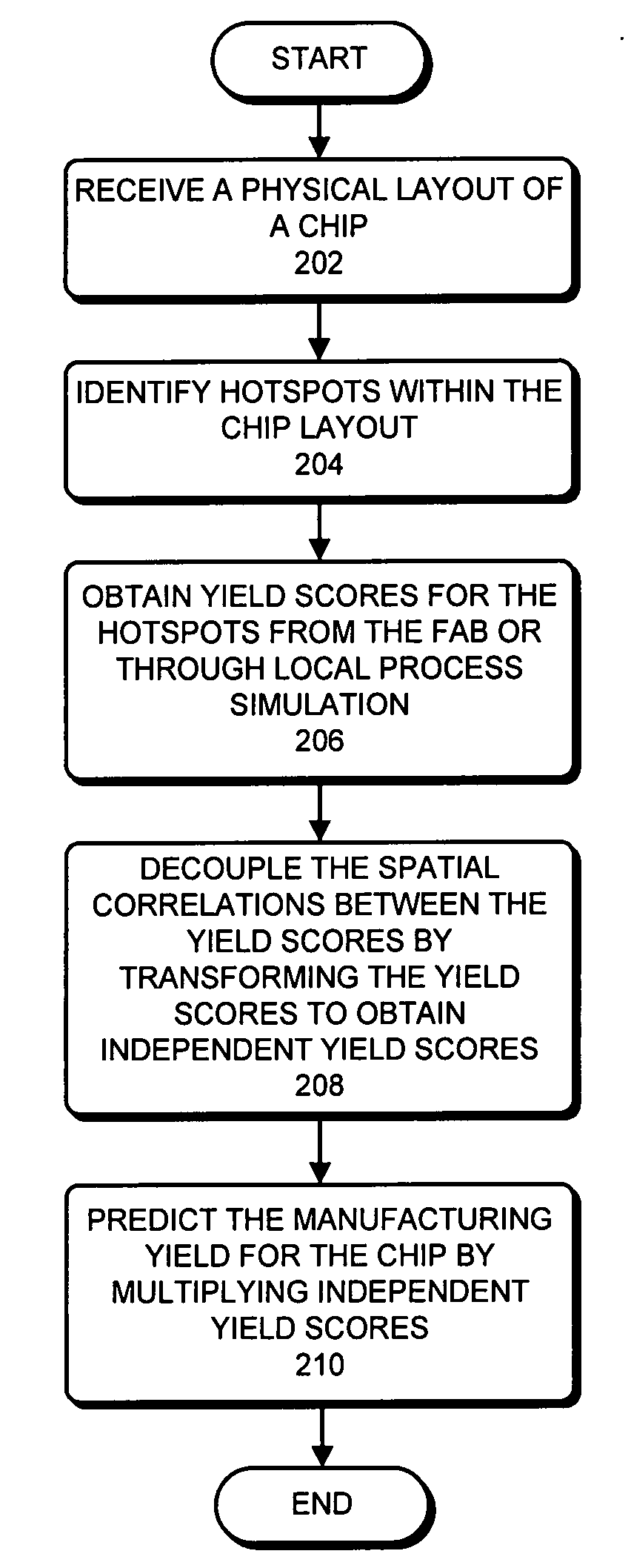
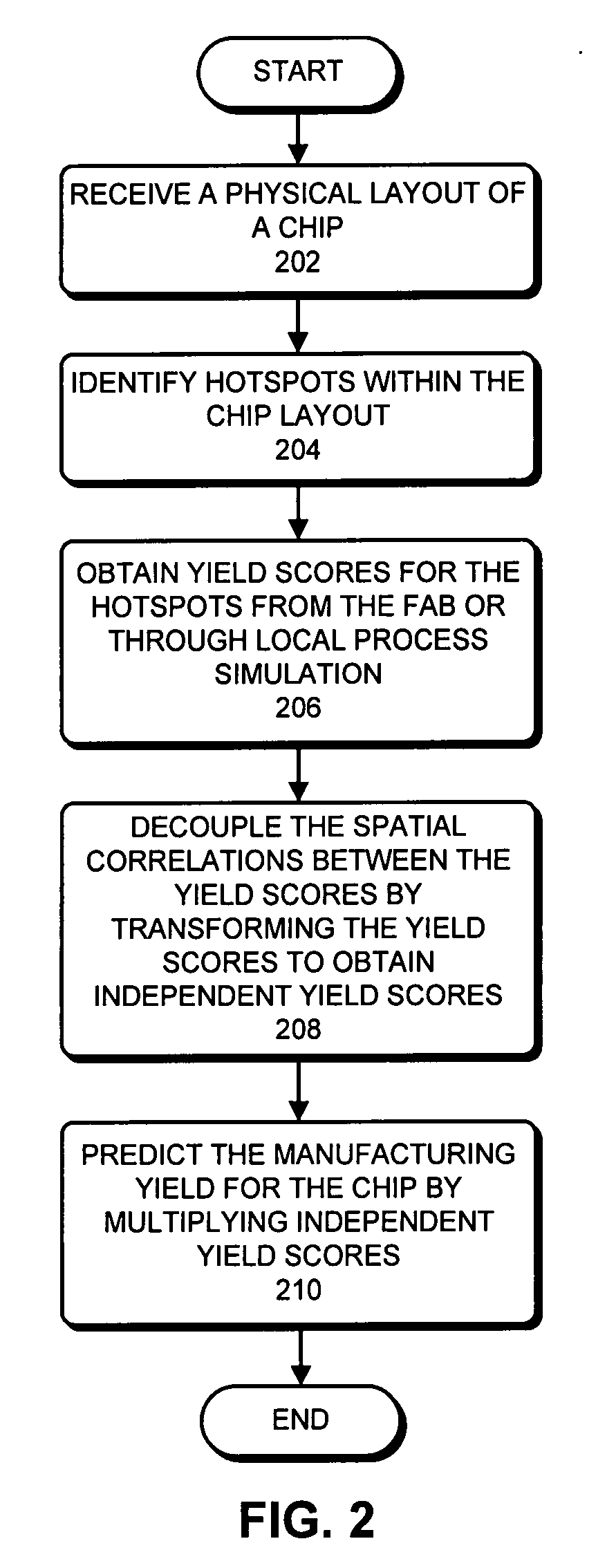
Predicting IC manufacturing yield based on hotspots
PatentActiveUS20080295046A1
Innovation
- A system that identifies hotspots in a chip layout by receiving hotspot definitions and performing local process simulations to generate yield-indicative-variable values, then applies transformations to yield scores to decouple spatial correlations, allowing for accurate prediction of manufacturing yield by multiplying independent transformed scores.

Advanced Process Node Manufacturing Standards
Advanced process node manufacturing standards represent the cornerstone of modern semiconductor fabrication, establishing critical benchmarks for achieving optimal VLSI chip yield through sophisticated Design for Manufacturing (DFM) techniques. These standards encompass comprehensive specifications that govern every aspect of manufacturing processes at cutting-edge technology nodes, typically ranging from 7nm to 3nm and beyond.
The evolution of manufacturing standards has been driven by the relentless pursuit of Moore's Law scaling, necessitating unprecedented precision in lithographic processes, material deposition, and etching techniques. Contemporary standards mandate extremely tight tolerances for critical dimensions, with variations measured in angstroms rather than nanometers. These specifications directly impact DFM implementation strategies, requiring designers to incorporate manufacturing constraints early in the design phase.
Process control standards have become increasingly sophisticated, incorporating real-time monitoring systems and advanced statistical process control methodologies. These frameworks establish acceptable ranges for key parameters such as line width roughness, overlay accuracy, and defect density thresholds. The integration of machine learning algorithms into process monitoring has enabled predictive maintenance and adaptive process optimization, significantly enhancing yield outcomes.
Material purity and handling standards have reached extraordinary levels of stringency, with contamination limits measured in parts per trillion for critical process chemicals. Clean room classifications have evolved to accommodate the extreme sensitivity of advanced nodes, with particle count specifications that exceed traditional ISO standards. These environmental controls are essential for maintaining the integrity of DFM-optimized designs throughout the manufacturing flow.
Metrology and inspection standards have advanced to support in-line monitoring of increasingly complex three-dimensional structures. Advanced techniques including high-resolution scanning electron microscopy, atomic force microscopy, and X-ray scattering methods are now standardized for process qualification and yield optimization. These measurement capabilities enable precise feedback loops that support continuous improvement in DFM methodologies.
The standardization of design rule checking and manufacturing rule compliance has become more sophisticated, incorporating probabilistic models that account for process variations and their impact on yield. These standards provide the foundation for implementing effective DFM techniques that maximize manufacturing success rates while maintaining design performance objectives.
Cost-Benefit Analysis of DFM Implementation
The implementation of Design for Manufacturing (DFM) techniques in VLSI chip production requires substantial upfront investment but delivers significant long-term financial returns through improved yield rates and reduced manufacturing costs. Initial capital expenditure typically includes advanced process simulation software, enhanced metrology equipment, and specialized training programs for engineering teams. These investments generally range from $2-5 million for mid-scale semiconductor facilities, with larger fabs requiring proportionally higher investments.
The primary cost drivers encompass software licensing for DFM tools, hardware upgrades for manufacturing equipment, and personnel training expenses. Additional costs include extended design cycle times during initial implementation phases and potential production delays as teams adapt to new methodologies. However, these short-term expenses are offset by substantial operational savings within 12-18 months of full implementation.
Quantifiable benefits emerge through dramatic yield improvements, with industry data showing 15-25% yield increases following comprehensive DFM adoption. For a typical 300mm wafer fab producing 1000 wafers monthly, this translates to approximately $3-8 million annual savings, depending on chip complexity and market value. Reduced rework costs contribute an additional 10-15% savings in manufacturing expenses.
Secondary benefits include shortened time-to-market cycles, improved product reliability, and enhanced competitive positioning. DFM implementation reduces design iterations by 30-40%, accelerating product launches and capturing market opportunities more effectively. The improved manufacturing predictability also enables better capacity planning and inventory management.
Return on investment calculations consistently demonstrate positive outcomes within 18-24 months for most semiconductor manufacturers. The cumulative financial impact over five years typically yields 300-500% ROI, making DFM implementation one of the most cost-effective manufacturing optimization strategies available to the semiconductor industry.
Unlock deeper insights with Patsnap Eureka Quick Research — get a full tech report to explore trends and direct your research. Try now!
Generate Your Research Report Instantly with AI Agent
Supercharge your innovation with Patsnap Eureka AI Agent Platform!