Achieve Zero Jitter with VLSI Clock Distribution Networks
MAR 7, 20269 MIN READ
Generate Your Research Report Instantly with AI Agent
PatSnap Eureka helps you evaluate technical feasibility & market potential.
VLSI Clock Jitter Challenges and Zero-Jitter Goals
VLSI clock distribution networks face unprecedented challenges as semiconductor technology advances toward nanometer scales and multi-gigahertz operating frequencies. Clock jitter, defined as the temporal variation of clock signal edges from their ideal positions, has emerged as one of the most critical performance-limiting factors in modern integrated circuits. This phenomenon manifests in various forms including period jitter, cycle-to-cycle jitter, and phase jitter, each contributing to timing uncertainties that can compromise circuit functionality and system reliability.
The evolution of VLSI technology has fundamentally transformed the nature of clock distribution challenges. Early integrated circuits operating at modest frequencies could tolerate significant timing variations without performance degradation. However, contemporary processors, high-speed memory interfaces, and communication systems demand timing precision measured in picoseconds or even femtoseconds. Process variations, supply voltage fluctuations, temperature gradients, and electromagnetic interference collectively contribute to jitter accumulation across complex clock trees spanning entire chip areas.
Traditional clock distribution architectures struggle to maintain timing integrity as design complexity increases exponentially. Multi-core processors with billions of transistors require synchronized operation across diverse functional blocks, each with unique power consumption patterns and thermal characteristics. The resulting dynamic variations in clock propagation delay create systematic and random jitter components that degrade overall system performance and increase power consumption through timing margin penalties.
Zero-jitter clock distribution represents the theoretical ideal where clock signals arrive at all destination points with perfect temporal precision, eliminating timing uncertainties that constrain system performance. This ambitious goal encompasses multiple technical objectives including minimizing clock skew variations, reducing supply-induced jitter, compensating for process and temperature variations, and maintaining signal integrity across global interconnects.
Achieving zero-jitter performance requires revolutionary approaches to clock generation, distribution, and compensation mechanisms. Advanced phase-locked loops with enhanced noise rejection, adaptive clock deskewing circuits, and real-time jitter monitoring systems form the foundation of next-generation solutions. Additionally, novel circuit topologies such as distributed clock generation, mesh-based distribution networks, and active jitter cancellation techniques promise significant improvements over conventional tree-based architectures.
The pursuit of zero-jitter clock distribution drives innovation across multiple technological domains, from advanced semiconductor processes optimized for timing precision to sophisticated electronic design automation tools capable of predicting and mitigating jitter sources during the design phase.
Market Demand for High-Performance Clock Distribution
The semiconductor industry's relentless pursuit of higher performance and lower power consumption has created an unprecedented demand for ultra-precise clock distribution systems. Modern processors, graphics processing units, and system-on-chip designs operate at frequencies exceeding several gigahertz, where even picosecond-level timing variations can cause catastrophic system failures. This stringent requirement has positioned zero-jitter clock distribution as a critical enabling technology for next-generation electronic systems.
High-frequency computing applications represent the largest market segment driving demand for advanced clock distribution networks. Data centers processing artificial intelligence workloads require synchronized operations across thousands of processing cores, where timing inconsistencies directly translate to computational errors and reduced throughput. Similarly, high-performance computing clusters used in scientific research and financial modeling depend on precise clock synchronization to maintain data integrity across distributed processing elements.
The telecommunications infrastructure sector has emerged as another significant demand driver, particularly with the global deployment of 5G networks and the anticipated transition to 6G technologies. Base station equipment, network processors, and optical communication systems require clock distribution networks capable of maintaining phase coherence across multiple signal processing chains. Any jitter introduction at the clock level propagates through the entire signal path, degrading communication quality and reducing network capacity.
Automotive electronics present a rapidly expanding market opportunity, especially with the proliferation of autonomous driving systems and advanced driver assistance technologies. Modern vehicles integrate dozens of electronic control units that must operate in perfect synchronization for safety-critical functions. The automotive industry's shift toward centralized computing architectures further amplifies the need for robust clock distribution solutions that can maintain timing accuracy across harsh operating environments.
Consumer electronics manufacturers face increasing pressure to deliver higher performance while reducing power consumption and form factor. Mobile processors, gaming consoles, and high-resolution display controllers all benefit from jitter-free clock distribution, which enables higher operating frequencies without compromising system stability. The market demand extends beyond traditional silicon-based solutions to include emerging technologies such as quantum processors and neuromorphic computing systems, where timing precision requirements are even more stringent.
The aerospace and defense sectors contribute additional market demand, driven by radar systems, satellite communications, and electronic warfare applications that require exceptional timing accuracy for mission-critical operations.
Current Jitter Issues in VLSI Clock Networks
Clock jitter represents one of the most critical performance bottlenecks in modern VLSI systems, manifesting as temporal variations in clock signal transitions that deviate from their ideal timing positions. In high-performance processors operating at multi-gigahertz frequencies, even picosecond-level jitter can significantly degrade system performance and reliability. The problem becomes increasingly severe as semiconductor technology scales down to advanced nodes below 7nm, where process variations and environmental factors amplify timing uncertainties.
Process-induced jitter emerges as a primary concern in contemporary VLSI designs. Manufacturing variations in transistor dimensions, threshold voltages, and interconnect geometries create systematic and random timing deviations across different regions of the chip. These variations are particularly pronounced in clock distribution networks spanning large die areas, where local process corners can vary significantly. The resulting clock skew and jitter directly impact setup and hold timing margins, forcing designers to adopt conservative timing constraints that limit overall system performance.
Power supply noise represents another major contributor to clock jitter in modern integrated circuits. Dynamic switching activities create voltage fluctuations on power distribution networks, which directly modulate clock buffer delays and transition times. As supply voltages continue to scale down with each technology generation, the relative impact of power supply noise on timing becomes more pronounced. Clock distribution networks, being among the highest activity circuits on chip, are particularly susceptible to supply-induced jitter effects.
Thermal variations across the die introduce additional timing uncertainties that compound jitter issues. Non-uniform power dissipation creates temperature gradients that affect transistor performance and interconnect resistance. Clock buffers operating at different temperatures exhibit varying propagation delays, contributing to both systematic skew and random jitter. The situation is exacerbated in high-performance processors where thermal hotspots can create localized timing variations exceeding several picoseconds.
Electromagnetic interference and substrate coupling present growing challenges in densely integrated systems. High-frequency switching activities in adjacent circuits couple through substrate and interconnect parasitics, injecting noise into sensitive clock distribution paths. This coupling becomes more severe as integration density increases and isolation structures become less effective at advanced technology nodes.
The cumulative effect of these jitter sources creates a complex timing environment where traditional clock distribution strategies struggle to maintain acceptable performance margins. Current industry practices often resort to over-designing clock networks with excessive buffering and conservative timing margins, resulting in increased power consumption and area overhead while still failing to achieve optimal jitter performance.
Existing Clock Jitter Reduction Solutions
01 Clock distribution network architecture design for jitter reduction
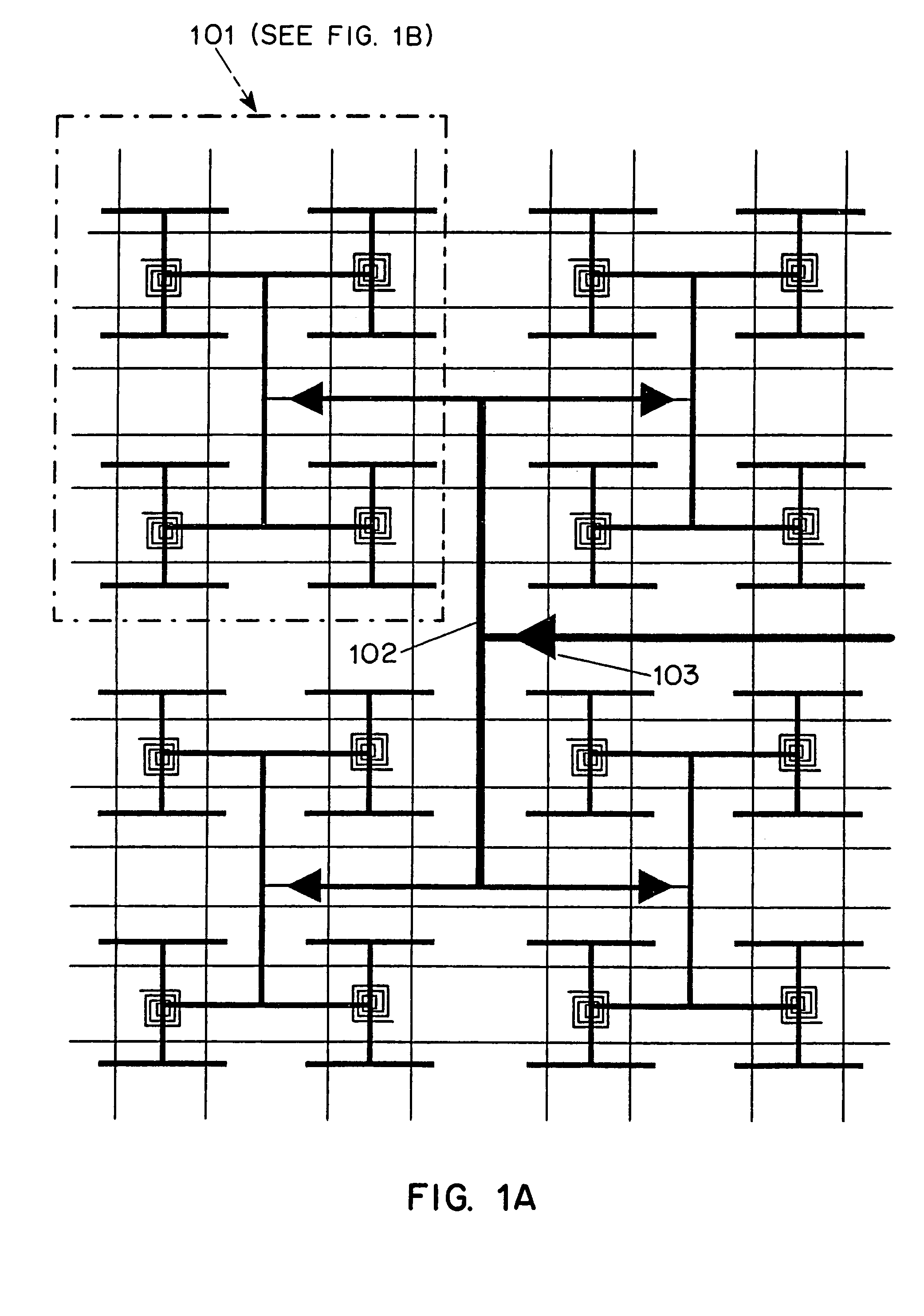
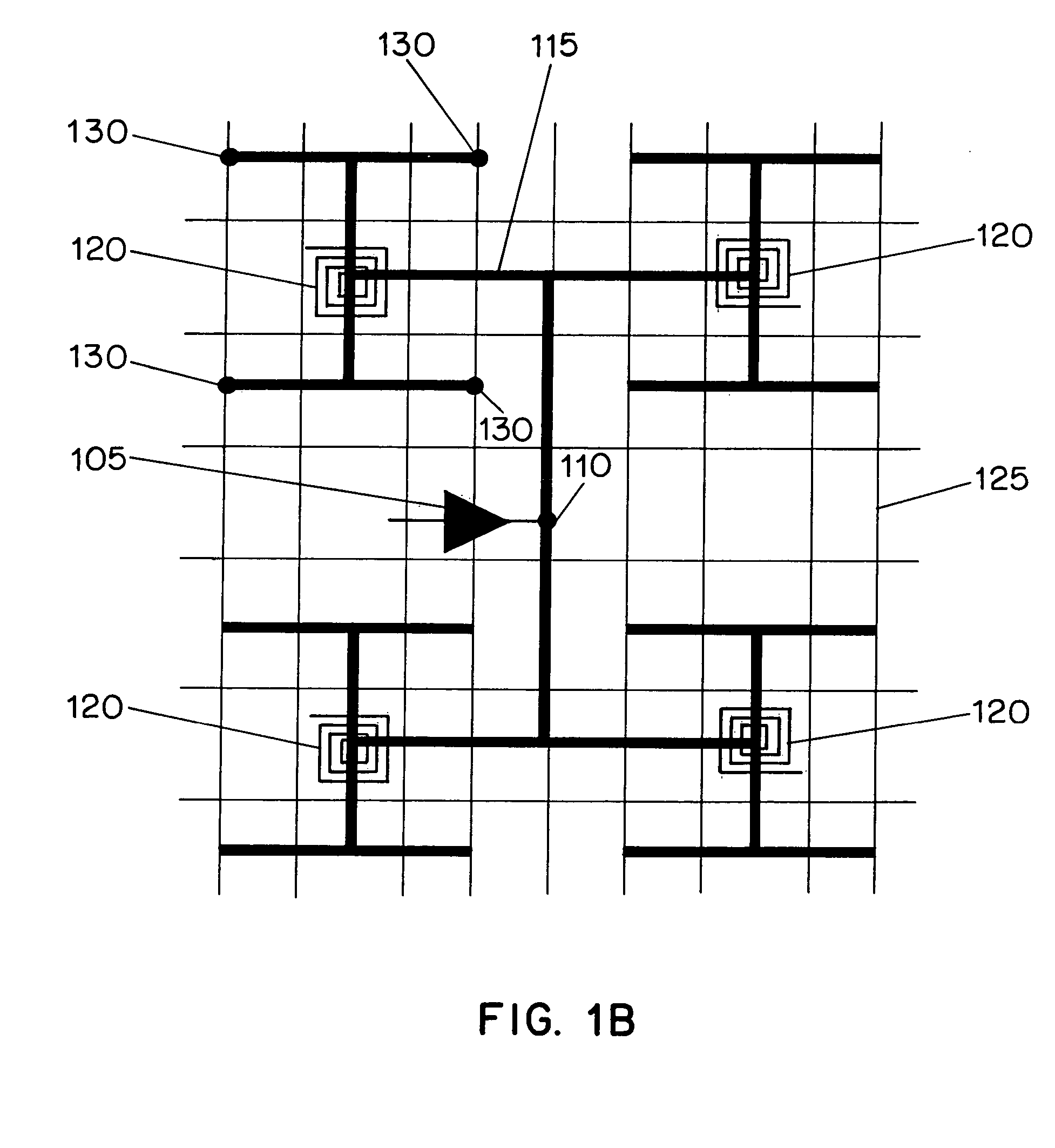
Various clock distribution network architectures can be designed to minimize jitter in VLSI systems. These architectures include tree-based structures, mesh networks, and hybrid topologies that balance signal propagation delays and reduce timing variations. The design considerations include buffer placement, wire routing strategies, and hierarchical distribution schemes to ensure uniform clock signal delivery across the chip while minimizing jitter accumulation.- Clock distribution network architecture design for jitter reduction: Various clock distribution network architectures can be designed to minimize jitter in VLSI systems. These architectures include tree-based structures, mesh networks, and hybrid topologies that balance signal propagation delays and reduce timing variations. The design focuses on optimizing the physical layout and routing of clock signals to ensure uniform distribution across the chip while minimizing skew and jitter. Advanced techniques involve careful buffer placement, wire sizing, and impedance matching to maintain signal integrity throughout the distribution network.
- Phase-locked loop (PLL) and delay-locked loop (DLL) circuits for jitter compensation: Phase-locked loops and delay-locked loops are essential circuits used to generate stable clock signals and compensate for jitter in clock distribution networks. These circuits can track and correct phase variations, providing clean clock signals with reduced jitter. The implementation includes feedback mechanisms that continuously adjust the clock phase to maintain synchronization and minimize timing errors. Advanced PLL and DLL designs incorporate jitter filtering capabilities and adaptive control algorithms to handle various sources of jitter in the system.
- Clock buffer and driver circuits with jitter mitigation: Specialized clock buffer and driver circuits are designed to amplify and distribute clock signals while minimizing the introduction of additional jitter. These circuits employ techniques such as differential signaling, controlled slew rates, and noise isolation to maintain signal quality. The buffer designs focus on reducing power supply noise sensitivity and improving common-mode rejection to prevent jitter accumulation through the distribution network. Advanced implementations include adaptive biasing and compensation circuits that adjust to process, voltage, and temperature variations.
- Jitter measurement and monitoring techniques: Various techniques and circuits are employed to measure and monitor jitter in clock distribution networks. These methods include time-to-digital converters, phase detectors, and statistical analysis circuits that can quantify different types of jitter including random jitter and deterministic jitter. The monitoring systems provide real-time feedback about clock signal quality and can trigger corrective actions when jitter exceeds acceptable thresholds. Advanced implementations integrate on-chip measurement capabilities that enable continuous monitoring during normal operation without disrupting system functionality.
- Power supply noise reduction for jitter minimization: Power supply noise is a significant contributor to jitter in clock distribution networks, and various techniques are employed to reduce its impact. These include dedicated power distribution networks for clock circuits, on-chip voltage regulators, and decoupling capacitor strategies. The designs focus on isolating sensitive clock circuits from noisy digital logic and providing clean, stable power supplies. Advanced implementations incorporate active noise cancellation, supply-independent biasing techniques, and shielding structures to minimize the coupling of power supply variations into clock signals.
02 Phase-locked loop (PLL) and delay-locked loop (DLL) circuits for jitter compensation
PLL and DLL circuits are widely used in clock distribution networks to compensate for jitter and maintain clock signal integrity. These circuits can lock onto reference clock signals and generate stable output clocks with reduced phase noise and timing variations. Advanced PLL and DLL designs incorporate jitter filtering mechanisms, adaptive bandwidth control, and multi-phase generation capabilities to improve overall system timing performance.Expand Specific Solutions03 Clock buffer and driver circuits with jitter mitigation
Specialized clock buffer and driver circuits are designed to minimize jitter introduction during signal amplification and distribution. These circuits employ techniques such as differential signaling, controlled slew rates, and noise-immune circuit topologies. The buffer designs focus on maintaining signal integrity while driving large capacitive loads across the clock distribution network, reducing both deterministic and random jitter components.Expand Specific Solutions04 Jitter measurement and monitoring techniques in clock networks
Various measurement and monitoring techniques are employed to detect and quantify jitter in clock distribution networks. These include time-to-digital converters, phase detectors, and built-in self-test circuits that can measure both cycle-to-cycle jitter and long-term jitter accumulation. Real-time monitoring capabilities enable adaptive compensation and provide feedback for dynamic jitter correction mechanisms.Expand Specific Solutions05 Adaptive and programmable clock distribution systems for jitter control
Adaptive clock distribution systems incorporate programmable elements and feedback mechanisms to dynamically adjust clock parameters and minimize jitter. These systems can modify delay elements, adjust buffer strengths, and reconfigure distribution paths based on operating conditions and measured jitter characteristics. The programmability allows for post-fabrication tuning and compensation of process variations that contribute to jitter.Expand Specific Solutions
Key Players in VLSI Clock Design Industry
The VLSI clock distribution network market for achieving zero jitter represents a mature yet rapidly evolving sector driven by increasing demands for high-performance computing and 5G infrastructure. The industry is experiencing significant growth with market leaders like Intel, Samsung Electronics, and Texas Instruments leveraging advanced semiconductor manufacturing capabilities to develop sophisticated clock management solutions. Technology maturity varies significantly across players, with established giants such as IBM, Micron Technology, and Renesas Electronics demonstrating proven expertise in precision timing circuits, while emerging companies like Socionext and specialized firms like IDT focus on innovative jitter reduction techniques. The competitive landscape includes both horizontal integration from major semiconductor manufacturers and vertical specialization from companies like Lattice Semiconductor and Advantest, creating a dynamic ecosystem where traditional timing solutions are being enhanced with AI-driven optimization and advanced process nodes to meet stringent jitter requirements.
Intel Corp.
Technical Solution: Intel employs advanced clock distribution architectures including H-tree and mesh topologies with precise buffer insertion and wire sizing optimization. Their approach utilizes clock gating techniques and dynamic voltage frequency scaling to minimize jitter propagation. Intel's processors implement multi-level clock distribution networks with dedicated phase-locked loops (PLLs) and delay-locked loops (DLLs) for each clock domain. They use statistical timing analysis and Monte Carlo simulations to predict and compensate for process variations that contribute to clock jitter. Additionally, Intel incorporates adaptive clock distribution circuits that can dynamically adjust to temperature and voltage variations in real-time.
Strengths: Industry-leading fabrication technology, extensive R&D resources, proven track record in high-performance processors. Weaknesses: High power consumption in complex clock networks, significant design complexity requiring specialized expertise.
International Business Machines Corp.
Technical Solution: IBM develops advanced clock distribution methodologies for high-performance computing systems using resonant clocking techniques and adiabatic switching to minimize power consumption and jitter. Their approach includes the implementation of rotary traveling wave oscillators and distributed amplification schemes for global clock distribution. IBM's Power processors utilize multi-phase clocking with precise phase relationships maintained through active phase interpolation circuits. They employ machine learning algorithms for predictive jitter compensation and implement adaptive clock mesh sizing based on workload characteristics. IBM also pioneers the use of optical clock distribution for inter-chip communication in large-scale systems, reducing electromagnetic interference and achieving unprecedented timing precision.
Strengths: Cutting-edge research capabilities, expertise in high-performance computing, innovative optical solutions. Weaknesses: Limited commercial availability of advanced technologies, high implementation complexity and cost.
Core Innovations in Zero-Jitter Clock Networks
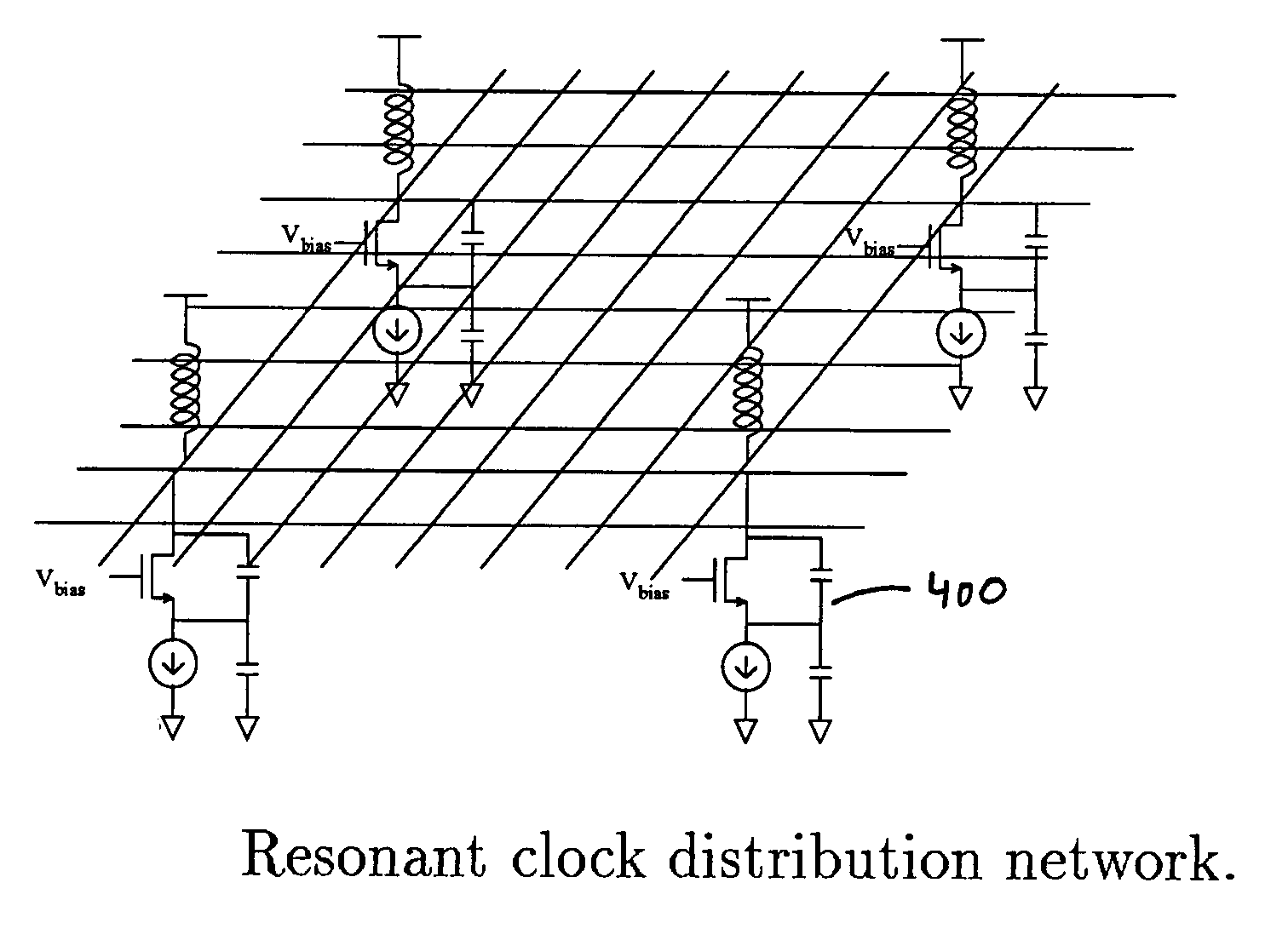
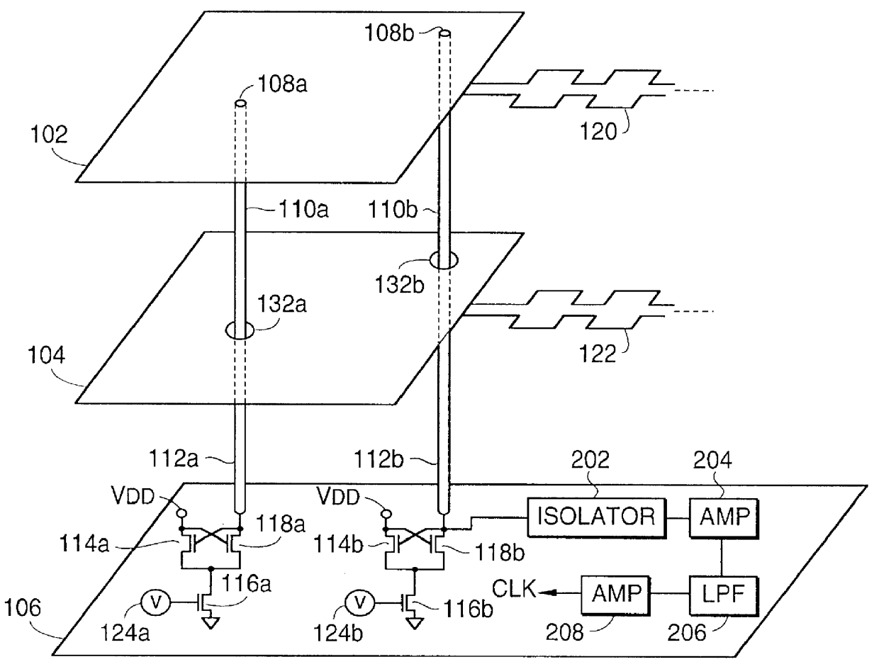
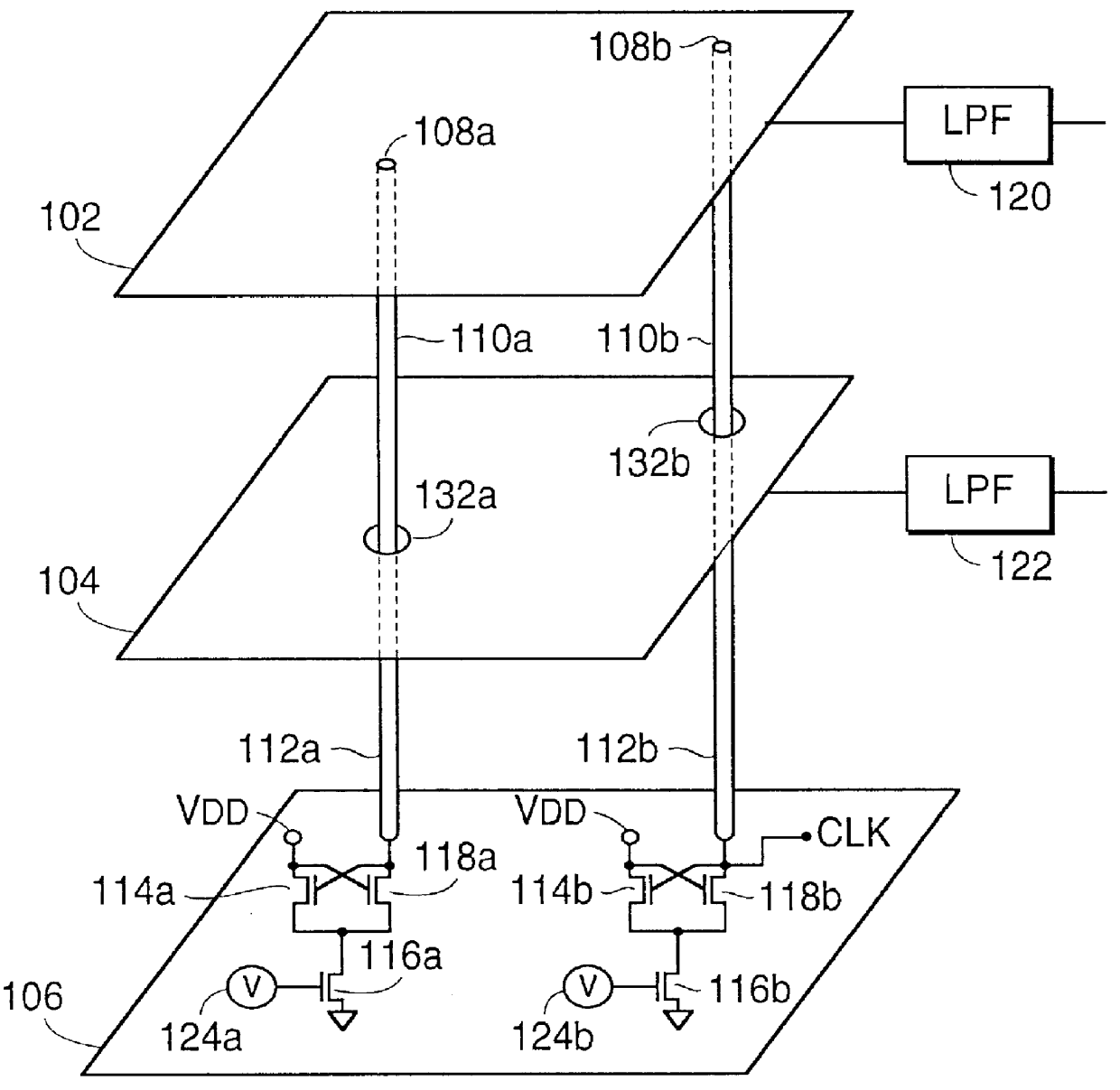
Resonant clock distribution for very large scale integrated circuits
PatentInactiveUS7015765B2
Innovation
- A capacitive clock distribution circuit with spiral inductors is used, which resonates with the clock circuit capacitance at the operating frequency, forming a resonant circuit that minimizes power consumption and reduces skew and jitter by distributing inductance throughout the grid and optimizing Q factor through selective capacitor switching.

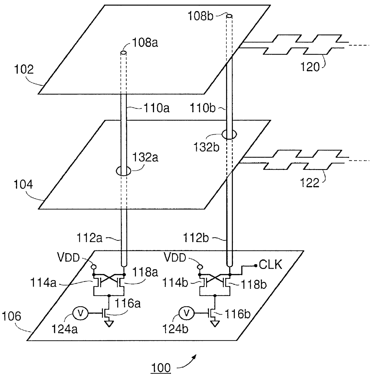
Method and apparatus for synchronized clock distribution
PatentInactiveUS6057724A
Innovation
- A distributed clock generator using a parallel plate microstrip patch resonator that produces a synchronized clock signal available at multiple points without propagation delay, eliminating the need for an external clock generator and allowing access on the interior surface of the resonator, thereby reducing clock skew.

Power Consumption Optimization in Clock Networks
Power consumption has emerged as a critical design constraint in modern VLSI clock distribution networks, particularly as semiconductor technology scales to nanometer dimensions. The relationship between power optimization and jitter performance creates a complex design space where traditional low-power techniques may inadvertently compromise timing precision. Clock networks typically consume 20-40% of total chip power in high-performance processors, making power reduction essential for thermal management and battery life extension in mobile applications.
Dynamic power consumption in clock networks stems primarily from the switching activity of clock buffers and the capacitive loading of interconnects. The power dissipated follows the relationship P = α × C × V² × f, where α represents activity factor, C denotes capacitance, V is supply voltage, and f indicates frequency. Minimizing these parameters while maintaining signal integrity requires sophisticated design methodologies that balance power efficiency with jitter constraints.
Supply voltage scaling represents the most effective power reduction technique, offering quadratic power savings. However, reduced voltage margins increase sensitivity to process variations and noise, potentially degrading jitter performance. Advanced power management strategies employ multiple voltage domains within clock networks, utilizing higher voltages for critical timing paths while applying aggressive scaling to non-critical branches.
Clock gating techniques provide substantial dynamic power savings by selectively disabling clock signals to inactive circuit blocks. Modern implementations utilize fine-grained gating at the register level, achieving power reductions of 50-70% in typical workloads. The challenge lies in implementing gating logic that introduces minimal skew and jitter while maintaining rapid enable/disable transitions.
Buffer sizing optimization plays a crucial role in power-jitter trade-offs. Oversized buffers consume excessive power while undersized buffers may introduce timing violations under process variations. Machine learning algorithms increasingly guide optimal buffer selection, considering statistical variations and power constraints simultaneously.
Emerging techniques include resonant clocking, which recovers energy from clock network capacitance, and near-threshold voltage operation combined with adaptive body biasing. These approaches promise significant power reductions while maintaining acceptable jitter levels through careful circuit design and real-time compensation mechanisms.
Thermal Management for Clock Distribution Systems
Thermal effects represent one of the most critical challenges in achieving zero jitter performance in VLSI clock distribution networks. As semiconductor devices continue to scale down and operating frequencies increase, power density within integrated circuits has grown exponentially, leading to significant thermal gradients across the chip surface. These temperature variations directly impact clock signal integrity through multiple mechanisms, creating substantial obstacles to maintaining precise timing synchronization.
Temperature fluctuations cause variations in transistor switching speeds, interconnect resistance, and propagation delays throughout the clock distribution tree. Even modest temperature differences of 10-15°C across a chip can result in timing skews of several picoseconds, which becomes increasingly problematic as target jitter specifications approach sub-picosecond levels. The relationship between temperature and delay is particularly pronounced in modern FinFET technologies, where threshold voltage sensitivity to temperature changes is amplified.
Effective thermal management strategies must address both steady-state temperature gradients and transient thermal effects. Steady-state management involves optimizing heat dissipation through advanced packaging solutions, thermal interface materials, and heat sink designs. Dynamic thermal management requires real-time monitoring and adaptive control mechanisms that can respond to rapid temperature changes caused by varying workloads and power consumption patterns.
Advanced thermal-aware clock distribution architectures incorporate temperature sensors strategically placed throughout the chip to provide feedback for adaptive timing control. These systems employ programmable delay elements and phase-locked loops that can compensate for thermally-induced timing variations in real-time. Additionally, thermal-aware floor planning techniques distribute heat-generating components more evenly, reducing peak temperatures and minimizing thermal gradients that contribute to clock jitter.
Emerging solutions include active thermal management using on-chip cooling mechanisms and predictive thermal modeling that anticipates temperature changes based on workload patterns. These approaches enable proactive compensation rather than reactive correction, significantly improving the overall thermal stability of clock distribution systems and supporting the achievement of zero jitter performance targets in next-generation VLSI designs.
Unlock deeper insights with PatSnap Eureka Quick Research — get a full tech report to explore trends and direct your research. Try now!
Generate Your Research Report Instantly with AI Agent
Supercharge your innovation with PatSnap Eureka AI Agent Platform!