

Atomic Layer Etching of 2D Materials for Nanoelectronics Applications
SEP 28, 20259 MIN READ
Generate Your Research Report Instantly with AI Agent
PatSnap Eureka helps you evaluate technical feasibility & market potential.
2D Materials ALE Technology Background and Objectives
Two-dimensional (2D) materials have emerged as promising candidates for next-generation nanoelectronics due to their unique physical properties, atomic thinness, and potential for extreme device scaling. Since the isolation of graphene in 2004, the family of 2D materials has expanded to include transition metal dichalcogenides (TMDs), hexagonal boron nitride (h-BN), black phosphorus, and MXenes, among others. These materials exhibit diverse electronic properties ranging from metallic to semiconducting and insulating behaviors, enabling a wide spectrum of applications in electronics, optoelectronics, and quantum computing.
Atomic Layer Etching (ALE) represents a critical fabrication technique for precisely manipulating 2D materials at the atomic scale. Unlike conventional etching methods that often cause significant damage to delicate 2D structures, ALE offers angstrom-level precision through self-limiting surface reactions. This technology has evolved from its initial applications in silicon processing to address the unique challenges presented by 2D materials, where even minor structural defects can dramatically alter electronic properties.
The historical development of ALE for 2D materials has been driven by the increasing demand for miniaturization in semiconductor devices and the limitations of traditional top-down fabrication approaches. Early attempts at processing 2D materials relied on adapted techniques from silicon technology, which often resulted in performance degradation due to lattice damage, edge roughness, and contamination. The evolution toward ALE methodologies began around 2015, with significant advancements occurring in the past five years as researchers recognized the need for more precise processing techniques.
Current ALE approaches for 2D materials typically involve cyclic processes with separate steps for surface modification and material removal. These techniques utilize carefully selected chemistries that interact selectively with specific atomic layers without disrupting underlying structures. Recent innovations include plasma-enhanced ALE, thermal ALE, and hybrid approaches that combine multiple mechanisms to achieve optimal results for different 2D material systems.
The primary objectives of advancing ALE technology for 2D materials include achieving atomic precision in lateral and vertical dimensions, minimizing process-induced defects, ensuring high selectivity between different 2D materials in heterostructures, and developing scalable processes compatible with industrial semiconductor manufacturing. Additionally, there is a growing focus on developing in-situ monitoring techniques to provide real-time feedback during the etching process.
Looking forward, the technology trajectory points toward integration of ALE with other atomic-scale fabrication methods such as Atomic Layer Deposition (ALD) to enable seamless processing of complex 2D material-based devices. The ultimate goal is to establish a comprehensive atomic-scale manufacturing paradigm that can fully harness the extraordinary properties of 2D materials for practical nanoelectronic applications, potentially enabling beyond-CMOS computing architectures.
Atomic Layer Etching (ALE) represents a critical fabrication technique for precisely manipulating 2D materials at the atomic scale. Unlike conventional etching methods that often cause significant damage to delicate 2D structures, ALE offers angstrom-level precision through self-limiting surface reactions. This technology has evolved from its initial applications in silicon processing to address the unique challenges presented by 2D materials, where even minor structural defects can dramatically alter electronic properties.
The historical development of ALE for 2D materials has been driven by the increasing demand for miniaturization in semiconductor devices and the limitations of traditional top-down fabrication approaches. Early attempts at processing 2D materials relied on adapted techniques from silicon technology, which often resulted in performance degradation due to lattice damage, edge roughness, and contamination. The evolution toward ALE methodologies began around 2015, with significant advancements occurring in the past five years as researchers recognized the need for more precise processing techniques.
Current ALE approaches for 2D materials typically involve cyclic processes with separate steps for surface modification and material removal. These techniques utilize carefully selected chemistries that interact selectively with specific atomic layers without disrupting underlying structures. Recent innovations include plasma-enhanced ALE, thermal ALE, and hybrid approaches that combine multiple mechanisms to achieve optimal results for different 2D material systems.
The primary objectives of advancing ALE technology for 2D materials include achieving atomic precision in lateral and vertical dimensions, minimizing process-induced defects, ensuring high selectivity between different 2D materials in heterostructures, and developing scalable processes compatible with industrial semiconductor manufacturing. Additionally, there is a growing focus on developing in-situ monitoring techniques to provide real-time feedback during the etching process.
Looking forward, the technology trajectory points toward integration of ALE with other atomic-scale fabrication methods such as Atomic Layer Deposition (ALD) to enable seamless processing of complex 2D material-based devices. The ultimate goal is to establish a comprehensive atomic-scale manufacturing paradigm that can fully harness the extraordinary properties of 2D materials for practical nanoelectronic applications, potentially enabling beyond-CMOS computing architectures.
Market Analysis for 2D Nanoelectronics Applications
The global market for 2D materials in nanoelectronics is experiencing unprecedented growth, driven by the increasing demand for smaller, faster, and more energy-efficient electronic devices. The market value for 2D materials in electronics applications reached approximately $12 million in 2022 and is projected to grow at a CAGR of 36% through 2030, potentially reaching $180 million by the end of the decade. This remarkable growth trajectory is primarily fueled by the unique properties of 2D materials that enable breakthrough performance in next-generation electronic devices.
The semiconductor industry's continuous push toward miniaturization, following Moore's Law, has created significant market opportunities for atomic layer etching (ALE) of 2D materials. Traditional silicon-based technologies are approaching their physical limits, creating a substantial market gap that 2D materials are positioned to fill. Market research indicates that over 70% of semiconductor manufacturers are actively investigating 2D materials for future product roadmaps.
Consumer electronics represents the largest current application segment, accounting for approximately 45% of the 2D nanoelectronics market. This is followed by telecommunications (25%), automotive electronics (15%), and healthcare devices (10%). The remaining 5% is distributed across various emerging applications. The demand for flexible electronics alone is expected to create a $40 million opportunity for 2D materials by 2028.
Geographically, North America leads the market with 38% share, followed by East Asia (particularly South Korea, Japan, and Taiwan) with 35%, Europe with 20%, and the rest of the world accounting for 7%. China is demonstrating the fastest growth rate, with investments in 2D materials research increasing by 42% annually over the past three years.
Key market drivers include the growing demand for flexible and wearable electronics, increasing investment in quantum computing research, and the expansion of IoT devices requiring ultra-low power consumption. The transition to 5G and future 6G technologies is also creating significant demand for high-frequency electronic components where 2D materials excel.
Market challenges include high production costs, with current manufacturing expenses for 2D material-based devices approximately 3-5 times higher than traditional silicon alternatives. Scalability remains another significant barrier, as most production methods are still limited to laboratory scales. Additionally, the market faces standardization issues, with competing material systems and processing techniques creating fragmentation.
The competitive landscape features both established semiconductor giants and specialized startups. Major players like Samsung, Intel, and TSMC have dedicated R&D divisions for 2D materials, while venture capital funding for 2D materials startups has reached $850 million in 2022 alone, a 65% increase from the previous year.
The semiconductor industry's continuous push toward miniaturization, following Moore's Law, has created significant market opportunities for atomic layer etching (ALE) of 2D materials. Traditional silicon-based technologies are approaching their physical limits, creating a substantial market gap that 2D materials are positioned to fill. Market research indicates that over 70% of semiconductor manufacturers are actively investigating 2D materials for future product roadmaps.
Consumer electronics represents the largest current application segment, accounting for approximately 45% of the 2D nanoelectronics market. This is followed by telecommunications (25%), automotive electronics (15%), and healthcare devices (10%). The remaining 5% is distributed across various emerging applications. The demand for flexible electronics alone is expected to create a $40 million opportunity for 2D materials by 2028.
Geographically, North America leads the market with 38% share, followed by East Asia (particularly South Korea, Japan, and Taiwan) with 35%, Europe with 20%, and the rest of the world accounting for 7%. China is demonstrating the fastest growth rate, with investments in 2D materials research increasing by 42% annually over the past three years.
Key market drivers include the growing demand for flexible and wearable electronics, increasing investment in quantum computing research, and the expansion of IoT devices requiring ultra-low power consumption. The transition to 5G and future 6G technologies is also creating significant demand for high-frequency electronic components where 2D materials excel.
Market challenges include high production costs, with current manufacturing expenses for 2D material-based devices approximately 3-5 times higher than traditional silicon alternatives. Scalability remains another significant barrier, as most production methods are still limited to laboratory scales. Additionally, the market faces standardization issues, with competing material systems and processing techniques creating fragmentation.
The competitive landscape features both established semiconductor giants and specialized startups. Major players like Samsung, Intel, and TSMC have dedicated R&D divisions for 2D materials, while venture capital funding for 2D materials startups has reached $850 million in 2022 alone, a 65% increase from the previous year.
Current ALE Challenges for 2D Materials
Despite significant advancements in Atomic Layer Etching (ALE) technology, several critical challenges persist when applying this technique to 2D materials for nanoelectronics applications. The atomically thin nature of 2D materials presents unique difficulties that conventional ALE processes struggle to address effectively.
One primary challenge is achieving precise layer-by-layer etching without damaging the underlying layers. Unlike bulk materials, 2D materials have extremely limited thickness tolerance, where even minor over-etching can completely destroy the functional layer. This requires unprecedented control over etch selectivity and uniformity that pushes current ALE technology to its limits.
The diverse chemical properties across different 2D materials further complicate the development of universal ALE processes. Materials like graphene, transition metal dichalcogenides (TMDs), and hexagonal boron nitride (h-BN) each require specific chemistry for effective etching. Current ALE techniques often lack the versatility to address this diversity without significant process modifications.
Interface management presents another significant hurdle. Many nanoelectronic applications utilize heterostructures of different 2D materials, and selectively etching one material without affecting adjacent layers remains extremely difficult. The weak van der Waals forces between layers create unique etch dynamics not encountered in traditional semiconductor processing.
Plasma-based ALE approaches face particular difficulties with 2D materials due to their susceptibility to plasma-induced damage. Even low-energy plasmas can introduce defects that dramatically alter the electronic properties of these materials. While thermal ALE offers a potential alternative, it currently lacks the precision required for nanoscale device fabrication in many 2D material systems.
Metrology and in-situ monitoring represent additional challenges. The atomically thin nature of 2D materials makes real-time process monitoring extremely difficult, limiting feedback control during etching. Current analytical techniques often cannot provide the necessary spatial and temporal resolution to effectively monitor the ALE process for 2D materials.
Scalability remains a significant barrier to industrial implementation. Laboratory-scale ALE processes for 2D materials typically involve slow processing rates and small sample sizes. Translating these processes to wafer-scale production while maintaining atomic-level precision presents substantial engineering challenges that have yet to be fully addressed.
Edge effects and anisotropic etching behavior further complicate ALE of 2D materials. The unique edge chemistry of 2D materials can lead to preferential etching along specific crystallographic directions, making it difficult to achieve the precise geometries required for advanced nanoelectronic devices.
One primary challenge is achieving precise layer-by-layer etching without damaging the underlying layers. Unlike bulk materials, 2D materials have extremely limited thickness tolerance, where even minor over-etching can completely destroy the functional layer. This requires unprecedented control over etch selectivity and uniformity that pushes current ALE technology to its limits.
The diverse chemical properties across different 2D materials further complicate the development of universal ALE processes. Materials like graphene, transition metal dichalcogenides (TMDs), and hexagonal boron nitride (h-BN) each require specific chemistry for effective etching. Current ALE techniques often lack the versatility to address this diversity without significant process modifications.
Interface management presents another significant hurdle. Many nanoelectronic applications utilize heterostructures of different 2D materials, and selectively etching one material without affecting adjacent layers remains extremely difficult. The weak van der Waals forces between layers create unique etch dynamics not encountered in traditional semiconductor processing.
Plasma-based ALE approaches face particular difficulties with 2D materials due to their susceptibility to plasma-induced damage. Even low-energy plasmas can introduce defects that dramatically alter the electronic properties of these materials. While thermal ALE offers a potential alternative, it currently lacks the precision required for nanoscale device fabrication in many 2D material systems.
Metrology and in-situ monitoring represent additional challenges. The atomically thin nature of 2D materials makes real-time process monitoring extremely difficult, limiting feedback control during etching. Current analytical techniques often cannot provide the necessary spatial and temporal resolution to effectively monitor the ALE process for 2D materials.
Scalability remains a significant barrier to industrial implementation. Laboratory-scale ALE processes for 2D materials typically involve slow processing rates and small sample sizes. Translating these processes to wafer-scale production while maintaining atomic-level precision presents substantial engineering challenges that have yet to be fully addressed.
Edge effects and anisotropic etching behavior further complicate ALE of 2D materials. The unique edge chemistry of 2D materials can lead to preferential etching along specific crystallographic directions, making it difficult to achieve the precise geometries required for advanced nanoelectronic devices.
Current ALE Process Solutions for 2D Materials
01 Atomic layer etching techniques for 2D materials
Atomic layer etching (ALE) techniques specifically designed for 2D materials involve precise removal of atomic layers with controlled selectivity. These techniques utilize cyclic processes of adsorption and removal steps to achieve atomic-level precision in etching. The methods enable manipulation of 2D material thickness with minimal damage to the underlying structure, which is crucial for maintaining the unique electronic and optical properties of these materials.- Plasma-based atomic layer etching techniques for 2D materials: Plasma-based atomic layer etching (ALE) techniques are used for precise removal of 2D material layers. These methods typically involve sequential exposure to reactive plasma species and purge steps to achieve controlled, layer-by-layer etching. The plasma parameters can be optimized to ensure selective etching of specific 2D materials while minimizing damage to underlying layers. This approach allows for nanoscale precision in fabricating devices based on 2D materials such as graphene, transition metal dichalcogenides, and other layered structures.
- Chemical vapor-based atomic layer etching for 2D materials: Chemical vapor-based atomic layer etching utilizes sequential exposure to reactive gases to achieve precise layer removal in 2D materials. This technique involves cycles of adsorption of reactive species followed by removal reactions, allowing for atomic-level control of the etching process. The method is particularly useful for sensitive 2D materials where plasma damage must be avoided. By carefully selecting reactive gases and process conditions, highly selective etching can be achieved while preserving the unique properties of the remaining 2D material layers.
- Thermal cycling methods for atomic layer etching of 2D materials: Thermal cycling methods involve alternating between heating and cooling cycles to facilitate controlled etching of 2D materials at the atomic scale. This approach relies on temperature-dependent reactions that allow for selective removal of atoms from the surface of 2D materials. The thermal energy provided during heating phases activates specific chemical reactions, while cooling phases help control the reaction rate and extent. This method is particularly valuable for temperature-sensitive 2D materials where maintaining structural integrity during processing is critical.
- Selective etching techniques for heterogeneous 2D material structures: Selective etching techniques are designed to target specific layers or components within heterogeneous 2D material structures. These methods exploit differences in chemical reactivity between various 2D materials to achieve high selectivity. By carefully selecting etchants and process conditions, it's possible to remove one type of 2D material while leaving others intact. This approach is crucial for fabricating complex heterostructures and devices that incorporate multiple types of 2D materials with different functionalities.
- Equipment and apparatus innovations for atomic layer etching of 2D materials: Specialized equipment and apparatus have been developed specifically for atomic layer etching of 2D materials. These innovations include custom reaction chambers, precise gas delivery systems, and advanced in-situ monitoring capabilities. The equipment is designed to provide the controlled environment necessary for atomic-precision etching, with features that enable precise timing of reactant exposure, uniform distribution of reactive species, and real-time process monitoring. These technological advances have been crucial in overcoming the challenges associated with processing atomically thin 2D materials.
02 Plasma-assisted atomic layer etching of 2D materials
Plasma-assisted atomic layer etching employs low-energy plasma to enhance the etching process of 2D materials. This approach combines chemical reactions with physical sputtering to achieve controlled layer-by-layer removal. The plasma parameters, including power, pressure, and gas composition, are carefully optimized to minimize damage while maintaining etching efficiency. This technique is particularly effective for materials like graphene, MoS2, and other transition metal dichalcogenides.Expand Specific Solutions03 Chemical vapor-based atomic layer etching methods
Chemical vapor-based atomic layer etching utilizes specific gas-phase reactants to selectively remove atomic layers from 2D materials. This approach relies on surface-limited reactions that occur in sequential steps, allowing for precise control over the etching depth. The process typically involves adsorption of reactive species, followed by a purge step and subsequent removal reaction. These methods offer high selectivity and can be performed at lower temperatures compared to traditional etching techniques.Expand Specific Solutions04 Equipment and apparatus for atomic layer etching of 2D materials
Specialized equipment and apparatus have been developed for atomic layer etching of 2D materials. These systems incorporate precise gas delivery mechanisms, temperature control, and in-situ monitoring capabilities to ensure accurate layer-by-layer removal. The equipment often features multiple chambers for different process steps, allowing for contamination-free transitions between etching cycles. Advanced reactor designs enable uniform etching across large substrate areas, which is essential for industrial applications.Expand Specific Solutions05 Integration of atomic layer etching in 2D material device fabrication
Atomic layer etching techniques are being integrated into the fabrication processes of devices based on 2D materials. This integration enables the creation of complex heterostructures, precise patterning, and controlled functionalization of 2D materials. The etching processes are designed to be compatible with other fabrication steps, such as deposition and lithography. This approach allows for the development of advanced electronic, optoelectronic, and sensing devices with enhanced performance characteristics.Expand Specific Solutions
Key Industry Players in ALE and 2D Nanoelectronics
The atomic layer etching (ALE) of 2D materials for nanoelectronics is in its early growth phase, with a rapidly expanding market projected to reach significant scale as 2D materials become critical for next-generation nanoelectronics. The competitive landscape is dominated by established semiconductor equipment manufacturers like Tokyo Electron, Lam Research, and Applied Materials, who possess advanced ALE technology platforms. Academic institutions including Jilin University, Caltech, and Yale University are driving fundamental research, while Samsung Electronics and BASF contribute materials expertise. The technology is approaching commercial maturity with key players focusing on precision control at atomic scales, selective etching processes, and integration with existing semiconductor manufacturing workflows to enable practical applications in future nanoelectronic devices.
Tokyo Electron Ltd.
Technical Solution: Tokyo Electron (TEL) has developed advanced Atomic Layer Etching (ALE) technology specifically optimized for 2D materials processing. Their approach utilizes a cyclic process with separate modification and removal steps that provides atomic-level precision control. TEL's ALE platform incorporates plasma-enhanced modification phases where the surface of 2D materials (like graphene, MoS2, and WSe2) is carefully activated, followed by selective removal steps using precisely controlled reactive gases. Their system achieves etch rates of approximately 0.2-0.3 Å per cycle while maintaining the crystalline structure and electronic properties of the remaining 2D material layers. TEL has integrated in-situ metrology tools that provide real-time feedback on layer thickness and surface quality, enabling closed-loop process control for enhanced repeatability across 300mm wafers. This technology has demonstrated damage-free etching with less than 1nm roughness on processed 2D material surfaces.
Strengths: Exceptional precision with atomic-level control, minimal damage to remaining layers, excellent uniformity across large wafers, and integrated metrology for real-time process monitoring. Weaknesses: Relatively slow etch rates compared to conventional methods, complex process parameter optimization required for different 2D materials, and higher cost of ownership compared to traditional etching equipment.
Lam Research Corp.
Technical Solution: Lam Research has pioneered a directional Atomic Layer Etching (ALE) technology specifically engineered for 2D materials nanoelectronics applications. Their approach combines precisely controlled plasma pulses with specialized chemistry cycles to achieve layer-by-layer removal of 2D materials while preserving the underlying layers' integrity. Lam's proprietary ALE process utilizes a sequential adsorption-reaction methodology where carefully selected precursors first modify the top atomic layer of materials like graphene or transition metal dichalcogenides (TMDs), followed by a selective removal step. Their system incorporates advanced RF power delivery systems that enable independent control of ion energy and flux, allowing for directional etching with minimal lateral damage. This technology has demonstrated sub-nanometer precision with etch rates controllable to approximately 0.1-0.2 nm per cycle, making it ideal for fabricating next-generation 2D material-based transistors, sensors, and quantum devices. Lam's ALE tools also feature sophisticated endpoint detection capabilities that can identify the completion of single atomic layer removal with high accuracy.
Strengths: Superior directional etching capability with minimal lateral spread, excellent damage control preserving electronic properties, and advanced process monitoring for precise endpoint detection. Weaknesses: Higher cost implementation compared to conventional etching techniques, relatively complex process integration requirements, and slower throughput than traditional etching methods which impacts manufacturing economics.
Critical Patents and Research in 2D Material ALE
Oxidation based atomic layer etching
PatentPendingUS20250232982A1
Innovation
- An atomic layer etching process involving cyclic oxidation, deposition of a protective layer, and selective etching is employed to form controlled openings in semiconductor materials, using non-corrosive precursors and etchants in a capacitively coupled plasma chamber, allowing for precise control of etch depth and sidewall profiles.


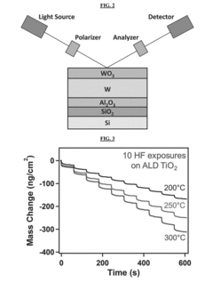
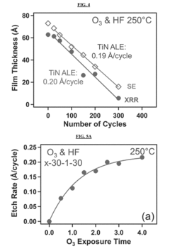
Atomic layer etching processes using sequential, self-limiting thermal reactions comprising oxidation and fluorination
PatentActiveUS10208383B2
Innovation
- A method involving sequential thermal reactions where a metal substrate is oxidized to form a self-passivating metal oxide layer, followed by fluorination to create a volatile metal fluoride, allowing for controlled atomic layer etching through the removal of these layers.


Material Compatibility and Integration Strategies
The integration of Atomic Layer Etching (ALE) with 2D materials presents unique challenges and opportunities that require careful consideration of material compatibility. Different 2D materials, including graphene, transition metal dichalcogenides (TMDs), and hexagonal boron nitride (h-BN), exhibit varying responses to ALE processes, necessitating tailored approaches for each material class.
For graphene-based nanoelectronics, ALE processes must preserve the exceptional electronic properties while achieving precise edge definition. Fluorine-based ALE chemistry has shown promising results, maintaining graphene's carrier mobility while enabling controlled layer removal. However, integration with conventional CMOS processes requires careful management of potential metal contamination and interfacial defects.
TMDs such as MoS2 and WSe2 demonstrate different etching behaviors compared to graphene due to their distinct chemical bonding characteristics. Hydrogen and halogen-based ALE processes have been developed specifically for these materials, but challenges remain in achieving uniform etching across wafer-scale areas. The integration strategy must account for the sensitivity of TMDs to oxygen and moisture exposure during transfer between process chambers.
Heterostructure integration presents additional complexity, as the ALE process optimized for one 2D material may damage adjacent layers in a vertical stack. Recent advances in selective ALE techniques utilize material-specific reaction pathways, enabling preferential etching of targeted layers while preserving others. This selectivity is crucial for fabricating complex 3D nanoelectronic architectures based on 2D material combinations.
The substrate choice significantly impacts ALE performance and subsequent device integration. Silicon, silicon dioxide, and hexagonal boron nitride substrates each present different interface dynamics during the etching process. Research indicates that h-BN substrates offer superior preservation of 2D material properties during ALE but introduce additional integration challenges with traditional semiconductor manufacturing lines.
Temperature management during ALE represents another critical integration consideration. While lower temperatures generally improve etching precision, they may limit reaction kinetics. Conversely, higher temperatures enhance reaction rates but risk damaging temperature-sensitive 2D materials or inducing unwanted diffusion at interfaces. Advanced thermal management strategies, including pulsed heating approaches, are being developed to optimize this trade-off.
Encapsulation techniques have emerged as effective strategies for protecting 2D materials during subsequent processing steps after ALE. Atomic layer deposition of dielectric materials immediately following the etching process can passivate reactive edges and prevent ambient degradation, though careful selection of encapsulation materials is required to avoid introducing strain or electronic perturbations.
For graphene-based nanoelectronics, ALE processes must preserve the exceptional electronic properties while achieving precise edge definition. Fluorine-based ALE chemistry has shown promising results, maintaining graphene's carrier mobility while enabling controlled layer removal. However, integration with conventional CMOS processes requires careful management of potential metal contamination and interfacial defects.
TMDs such as MoS2 and WSe2 demonstrate different etching behaviors compared to graphene due to their distinct chemical bonding characteristics. Hydrogen and halogen-based ALE processes have been developed specifically for these materials, but challenges remain in achieving uniform etching across wafer-scale areas. The integration strategy must account for the sensitivity of TMDs to oxygen and moisture exposure during transfer between process chambers.
Heterostructure integration presents additional complexity, as the ALE process optimized for one 2D material may damage adjacent layers in a vertical stack. Recent advances in selective ALE techniques utilize material-specific reaction pathways, enabling preferential etching of targeted layers while preserving others. This selectivity is crucial for fabricating complex 3D nanoelectronic architectures based on 2D material combinations.
The substrate choice significantly impacts ALE performance and subsequent device integration. Silicon, silicon dioxide, and hexagonal boron nitride substrates each present different interface dynamics during the etching process. Research indicates that h-BN substrates offer superior preservation of 2D material properties during ALE but introduce additional integration challenges with traditional semiconductor manufacturing lines.
Temperature management during ALE represents another critical integration consideration. While lower temperatures generally improve etching precision, they may limit reaction kinetics. Conversely, higher temperatures enhance reaction rates but risk damaging temperature-sensitive 2D materials or inducing unwanted diffusion at interfaces. Advanced thermal management strategies, including pulsed heating approaches, are being developed to optimize this trade-off.
Encapsulation techniques have emerged as effective strategies for protecting 2D materials during subsequent processing steps after ALE. Atomic layer deposition of dielectric materials immediately following the etching process can passivate reactive edges and prevent ambient degradation, though careful selection of encapsulation materials is required to avoid introducing strain or electronic perturbations.
Environmental Impact and Sustainability Considerations
The environmental impact of Atomic Layer Etching (ALE) for 2D materials represents a critical consideration as this technology advances toward widespread implementation in nanoelectronics. Compared to conventional etching processes, ALE demonstrates significant environmental advantages through its precise material removal capabilities. By eliminating only atomic layers with exceptional selectivity, ALE substantially reduces chemical waste generation and hazardous byproducts that typically result from traditional etching methods.
Energy efficiency constitutes another key environmental benefit of ALE processes. The technique's room-temperature operation capability for many 2D materials significantly decreases the energy requirements compared to high-temperature plasma etching processes. This reduced energy footprint directly translates to lower carbon emissions throughout the manufacturing lifecycle, aligning with global sustainability initiatives in semiconductor fabrication.
Chemical usage optimization represents a fundamental sustainability advantage of ALE. The process employs precisely controlled chemical reactions that require substantially smaller quantities of reactive gases and precursors. This reduction in chemical consumption not only decreases environmental contamination risks but also minimizes the extraction and processing demands for these specialized materials, many of which involve energy-intensive production methods.
Water conservation emerges as an additional environmental benefit, as ALE processes typically require less water for rinsing and cleaning steps compared to conventional wet etching techniques. This aspect becomes increasingly important considering the semiconductor industry's historically high water consumption rates and growing concerns about global water scarcity.
End-of-life considerations for 2D material-based nanoelectronics also warrant attention. The atomic precision of ALE potentially enables more effective material separation during recycling processes, facilitating the recovery of valuable elements from discarded electronic devices. This capability could significantly contribute to circular economy principles within the electronics industry.
Despite these advantages, several environmental challenges persist. The specialized gases used in certain ALE processes, particularly fluorine-containing compounds, may exhibit high global warming potential. Additionally, while individual ALE processes consume less energy, the cumulative energy requirements for multiple ALE cycles in manufacturing settings require careful assessment to ensure genuine sustainability benefits.
Future research directions should prioritize developing completely halogen-free ALE processes, implementing closed-loop chemical recycling systems, and establishing comprehensive lifecycle assessment methodologies specifically tailored for 2D material nanoelectronics. These efforts will ensure that environmental sustainability remains central to technological advancement in this rapidly evolving field.
Energy efficiency constitutes another key environmental benefit of ALE processes. The technique's room-temperature operation capability for many 2D materials significantly decreases the energy requirements compared to high-temperature plasma etching processes. This reduced energy footprint directly translates to lower carbon emissions throughout the manufacturing lifecycle, aligning with global sustainability initiatives in semiconductor fabrication.
Chemical usage optimization represents a fundamental sustainability advantage of ALE. The process employs precisely controlled chemical reactions that require substantially smaller quantities of reactive gases and precursors. This reduction in chemical consumption not only decreases environmental contamination risks but also minimizes the extraction and processing demands for these specialized materials, many of which involve energy-intensive production methods.
Water conservation emerges as an additional environmental benefit, as ALE processes typically require less water for rinsing and cleaning steps compared to conventional wet etching techniques. This aspect becomes increasingly important considering the semiconductor industry's historically high water consumption rates and growing concerns about global water scarcity.
End-of-life considerations for 2D material-based nanoelectronics also warrant attention. The atomic precision of ALE potentially enables more effective material separation during recycling processes, facilitating the recovery of valuable elements from discarded electronic devices. This capability could significantly contribute to circular economy principles within the electronics industry.
Despite these advantages, several environmental challenges persist. The specialized gases used in certain ALE processes, particularly fluorine-containing compounds, may exhibit high global warming potential. Additionally, while individual ALE processes consume less energy, the cumulative energy requirements for multiple ALE cycles in manufacturing settings require careful assessment to ensure genuine sustainability benefits.
Future research directions should prioritize developing completely halogen-free ALE processes, implementing closed-loop chemical recycling systems, and establishing comprehensive lifecycle assessment methodologies specifically tailored for 2D material nanoelectronics. These efforts will ensure that environmental sustainability remains central to technological advancement in this rapidly evolving field.
Unlock deeper insights with PatSnap Eureka Quick Research — get a full tech report to explore trends and direct your research. Try now!
Generate Your Research Report Instantly with AI Agent
Supercharge your innovation with PatSnap Eureka AI Agent Platform!