

Calibrate Assembly Processes for Substrate-Like PCBs
APR 22, 20269 MIN READ
Generate Your Research Report Instantly with AI Agent
Patsnap Eureka helps you evaluate technical feasibility & market potential.
Substrate-Like PCB Assembly Calibration Background and Objectives
Substrate-like PCBs represent a critical evolution in electronic packaging technology, bridging the gap between traditional printed circuit boards and advanced semiconductor substrates. These components feature ultra-fine pitch interconnects, typically ranging from 40 to 100 micrometers, and incorporate advanced materials such as low-loss dielectrics and embedded components. The manufacturing complexity of substrate-like PCBs demands unprecedented precision in assembly processes, particularly in component placement, soldering, and interconnection formation.
The assembly of substrate-like PCBs presents unique challenges due to their hybrid nature, combining characteristics of both PCB and IC substrate technologies. Traditional PCB assembly processes often prove inadequate for handling the microscopic features and tight tolerances required. The substrate-like architecture typically incorporates multiple layers with varying thermal expansion coefficients, creating assembly complexities that require specialized calibration approaches to ensure reliable interconnections and prevent warpage-induced failures.
Historical development in this field has been driven by the semiconductor industry's relentless pursuit of miniaturization and performance enhancement. The transition from wire bonding to flip-chip technologies, followed by the emergence of 2.5D and 3D packaging architectures, has necessitated the development of substrate-like PCB solutions. These platforms enable high-density interconnections while maintaining cost-effectiveness compared to pure semiconductor substrates.
Current assembly calibration challenges stem from the multi-scale nature of substrate-like PCBs, where macro-level board handling must coexist with micro-level precision requirements. Thermal management during assembly becomes critical due to the presence of sensitive embedded components and the risk of delamination between dissimilar materials. Additionally, the optical inspection and measurement systems used in traditional PCB assembly often lack the resolution required for substrate-like features.
The primary objective of developing robust calibration processes for substrate-like PCB assembly is to achieve consistent, high-yield manufacturing while maintaining the performance advantages these platforms offer. This includes establishing precise placement accuracy for ultra-fine pitch components, optimizing reflow profiles for complex material stacks, and implementing real-time process monitoring capabilities. The calibration framework must address both equipment-level precision and process-level repeatability to ensure scalable manufacturing solutions.
Success in this domain requires integration of advanced metrology systems, adaptive process control algorithms, and comprehensive understanding of material behavior under assembly conditions. The ultimate goal is to enable reliable mass production of substrate-like PCBs that meet the stringent requirements of next-generation electronic systems while maintaining economic viability for widespread adoption across various application domains.
Market Demand for High-Precision Substrate-Like PCB Assembly
The global electronics industry is experiencing unprecedented demand for high-precision substrate-like PCB assembly solutions, driven by the rapid advancement of miniaturization technologies and the proliferation of high-performance electronic devices. This market segment encompasses applications in smartphones, tablets, wearable devices, automotive electronics, and advanced computing systems where traditional PCB technologies cannot meet the stringent requirements for density, performance, and reliability.
Consumer electronics manufacturers are increasingly adopting substrate-like PCB technologies to achieve thinner form factors and enhanced electrical performance in their flagship products. The smartphone industry, in particular, has become a primary driver of this demand as manufacturers compete to deliver devices with improved processing power, extended battery life, and advanced camera systems within increasingly compact designs. These requirements necessitate assembly processes capable of handling ultra-fine pitch components and achieving exceptional placement accuracy.
The automotive sector represents another significant growth area, with the transition toward electric vehicles and autonomous driving systems creating substantial demand for high-precision electronic assemblies. Advanced driver assistance systems, battery management units, and infotainment systems require substrate-like PCBs that can operate reliably under harsh environmental conditions while maintaining precise electrical characteristics. This has led to increased investment in calibrated assembly processes that can ensure consistent quality and performance.
Data center and high-performance computing applications are driving demand for substrate-like PCBs capable of supporting high-speed signal transmission and thermal management. Server processors, graphics processing units, and networking equipment require assembly processes with exceptional precision to maintain signal integrity and prevent performance degradation. The growing adoption of artificial intelligence and machine learning technologies has further intensified these requirements.
Medical device manufacturers are increasingly recognizing the value of substrate-like PCB assembly for developing next-generation diagnostic and therapeutic equipment. Portable medical devices, implantable systems, and advanced imaging equipment require the miniaturization and reliability benefits that properly calibrated assembly processes can deliver. Regulatory requirements in this sector also emphasize the importance of consistent, validated manufacturing processes.
The aerospace and defense industries continue to demand high-precision assembly solutions for mission-critical applications where failure is not acceptable. Satellite systems, avionics, and military communication equipment require substrate-like PCBs assembled with processes that can guarantee long-term reliability under extreme operating conditions.
Market research indicates that the demand for calibrated assembly processes is being driven not only by the need for higher precision but also by the requirement for improved process control and traceability. Manufacturers are seeking solutions that can provide real-time monitoring, adaptive correction capabilities, and comprehensive documentation to meet quality standards and regulatory requirements across various industries.
Current Challenges in Substrate-Like PCB Assembly Calibration
Substrate-like PCBs present unique calibration challenges due to their ultra-thin profiles and high-density interconnect structures. Traditional calibration methods designed for conventional PCBs often prove inadequate when dealing with substrates that typically measure between 50-200 micrometers in thickness. The reduced structural rigidity creates significant warpage and dimensional instability during assembly processes, making it extremely difficult to maintain consistent positioning accuracy across the entire substrate surface.
Thermal management during assembly calibration represents another critical challenge. Substrate-like PCBs exhibit different thermal expansion coefficients compared to standard PCBs, leading to unpredictable dimensional changes during reflow processes. The calibration systems must account for these thermal variations, but current methodologies lack the precision required to compensate for the minute thermal-induced displacements that can cause assembly failures in high-density applications.
Component placement accuracy becomes exponentially more challenging with substrate-like PCBs due to their fine-pitch requirements. Traditional vision systems struggle to maintain the sub-micron precision needed for accurate component alignment on these ultra-thin substrates. The optical properties of substrate materials can interfere with standard fiducial recognition algorithms, leading to calibration errors that propagate throughout the assembly process.
Process repeatability poses significant obstacles in substrate-like PCB assembly calibration. The inherent flexibility of these thin substrates means that mechanical handling during calibration can introduce variations that are difficult to predict and compensate for. Standard calibration fixtures designed for rigid PCBs cannot adequately support substrate-like boards without causing deformation, which directly impacts the accuracy of calibration measurements.
Multi-layer registration accuracy presents additional complexity in calibration procedures. Substrate-like PCBs often feature multiple thin layers with critical interlayer alignment requirements. Calibration systems must verify not only surface-level positioning but also ensure proper registration between internal layers, which requires advanced measurement techniques that exceed the capabilities of conventional calibration equipment.
Environmental sensitivity further complicates calibration efforts. Substrate-like PCBs are highly susceptible to humidity and temperature fluctuations during the calibration process. These environmental factors can cause dimensional changes that occur faster than traditional calibration cycles can accommodate, necessitating real-time compensation mechanisms that current systems typically lack.
Existing Calibration Solutions for Substrate-Like PCB Assembly
01 Automated optical inspection and calibration systems for PCB assembly
Advanced optical inspection systems are employed to detect and calibrate component placement accuracy during PCB assembly processes. These systems utilize high-resolution cameras and image processing algorithms to identify misalignments, measure component positions, and provide feedback for real-time calibration adjustments. The automated inspection ensures precise component placement and reduces assembly defects.- Automated optical inspection and calibration systems for PCB assembly: Advanced optical inspection systems are employed to detect and calibrate component placement accuracy during PCB assembly processes. These systems utilize high-resolution cameras and image processing algorithms to identify misalignments, measure component positions, and provide feedback for real-time calibration adjustments. The automated inspection ensures precise component placement and reduces assembly defects.
- Vision-based alignment and positioning calibration methods: Vision-based calibration techniques use pattern recognition and fiducial marks on substrates to establish accurate reference coordinates for component placement. These methods involve capturing images of alignment marks, calculating position offsets, and adjusting placement equipment parameters accordingly. The calibration process compensates for mechanical variations and thermal expansion effects in the assembly line.
- Multi-point measurement and coordinate transformation for assembly calibration: Calibration approaches utilizing multiple measurement points across the substrate surface to establish coordinate transformation matrices. These techniques measure reference positions at various locations, calculate transformation parameters, and apply corrections to compensate for substrate warpage, rotation, and scaling errors. The multi-point calibration improves placement accuracy across the entire assembly area.
- Real-time feedback control and adaptive calibration systems: Dynamic calibration systems that continuously monitor assembly parameters and adjust equipment settings in real-time. These systems collect data from sensors during the assembly process, analyze deviations from target values, and automatically update calibration parameters to maintain optimal accuracy. The adaptive approach compensates for environmental changes and equipment drift during production.
- Substrate warpage compensation and height calibration techniques: Specialized calibration methods addressing substrate flatness variations and height differences in PCB assembly. These techniques measure substrate surface topology, calculate height profiles, and adjust component placement head positions accordingly. The compensation mechanisms ensure consistent component-to-substrate contact and solder joint quality despite substrate warpage or thickness variations.
02 Calibration methods using reference substrates and fiducial marks
Reference substrates with known patterns and fiducial marks are utilized to calibrate PCB assembly equipment. The system recognizes these reference points to establish coordinate systems and compensate for positioning errors. This calibration approach enables accurate alignment between the assembly machine's coordinate system and the actual substrate position, improving placement precision across different substrate types.Expand Specific Solutions03 Vision-based alignment and positioning correction systems
Vision-based systems capture images of substrates and components to determine their actual positions and orientations. Through pattern recognition and coordinate transformation algorithms, these systems calculate positioning deviations and generate correction parameters. The calibration data is then applied to adjust pick-and-place operations, ensuring accurate component mounting even when substrate positioning varies.Expand Specific Solutions04 Multi-point calibration and coordinate transformation techniques
Multi-point calibration methods establish mathematical relationships between machine coordinates and substrate coordinates by measuring multiple reference points. These techniques employ coordinate transformation matrices to compensate for linear and rotational offsets, scaling errors, and substrate warpage. The calibration process enhances positioning accuracy across the entire working area of the assembly system.Expand Specific Solutions05 Real-time feedback and adaptive calibration during assembly
Real-time monitoring systems continuously track assembly parameters and component placement results during production. Based on detected deviations, adaptive calibration algorithms automatically adjust machine parameters to maintain optimal accuracy. This dynamic calibration approach compensates for thermal drift, mechanical wear, and other time-varying factors that affect assembly precision.Expand Specific Solutions
Key Players in Substrate-Like PCB Manufacturing Industry
The substrate-like PCB assembly calibration market represents a mature technology sector experiencing steady growth driven by increasing demand for high-density interconnect solutions in consumer electronics, automotive, and telecommunications applications. The competitive landscape is dominated by established Asian manufacturers including Samsung Electro-Mechanics, SK Hynix, and LG Display, who leverage advanced manufacturing capabilities and vertical integration strategies. Technology maturity varies significantly across market segments, with companies like Texas Instruments, Intel, and Applied Materials leading in semiconductor integration and precision manufacturing equipment, while specialized firms such as Shengyi Electronics and i3 Electronics focus on advanced PCB fabrication techniques. The market demonstrates strong consolidation around key players who possess both manufacturing scale and R&D capabilities necessary for next-generation substrate technologies.
Samsung Electro-Mechanics Co., Ltd.
Technical Solution: Samsung Electro-Mechanics has developed advanced calibration methodologies for substrate-like PCB assembly processes, focusing on high-density interconnect (HDI) technology and embedded component substrates. Their approach integrates automated optical inspection (AOI) systems with real-time process monitoring to ensure precise component placement and solder joint quality. The company employs statistical process control (SPC) methods combined with machine learning algorithms to continuously optimize assembly parameters such as pick-and-place accuracy, reflow temperature profiles, and via filling processes. Their calibration framework includes comprehensive thermal management solutions and advanced materials characterization to handle the complex thermal expansion coefficients inherent in substrate-like PCB structures.
Strengths: Industry-leading HDI technology expertise, comprehensive thermal management solutions, advanced AOI integration. Weaknesses: High implementation costs, complex setup requirements for smaller manufacturers.
Texas Instruments Incorporated
Technical Solution: Texas Instruments has developed sophisticated calibration protocols specifically designed for substrate-like PCB assembly processes used in their semiconductor packaging operations. Their methodology incorporates precision measurement systems that monitor critical parameters including component placement accuracy, solder paste volume control, and thermal profile optimization during reflow processes. The calibration framework utilizes advanced metrology tools combined with statistical analysis software to establish process windows and control limits. TI's approach emphasizes real-time feedback control systems that automatically adjust assembly parameters based on continuous monitoring of key quality indicators such as joint strength, electrical continuity, and thermal performance characteristics.
Strengths: Robust statistical analysis capabilities, real-time feedback control systems, extensive semiconductor packaging expertise. Weaknesses: Limited applicability outside semiconductor industry, requires specialized equipment and training.
Core Calibration Innovations for Substrate-Like PCB Processes
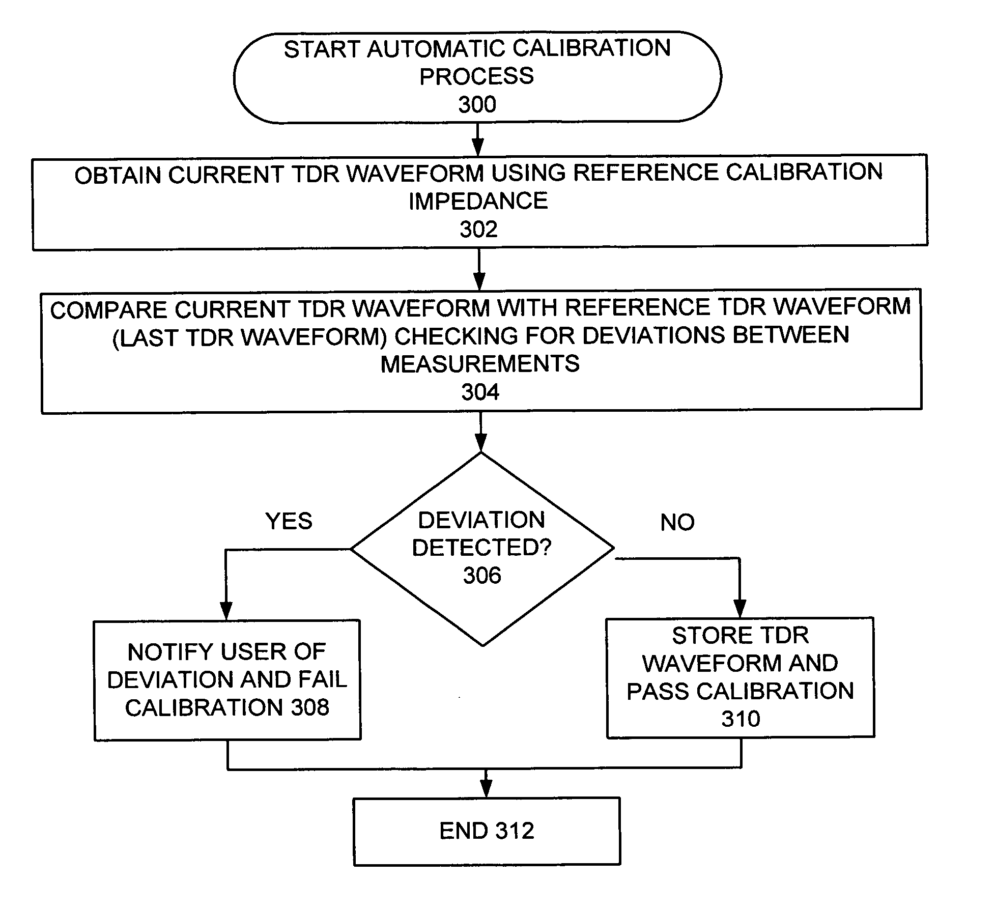
Method and apparatus for implementing automatic-calibration of TDR probing system
PatentInactiveUS20070143050A1
Innovation
- An automatic calibration method and apparatus for Time Domain Reflectometer (TDR) probing apparatus that compares current and reference waveforms using a known impedance standard, notifying users of deviations and ensuring continuous calibration without user intervention, utilizing an enhanced TDR probe integrated with a computer test system.

Printed circuit board calibrating system
PatentActiveTW202020694A
Innovation
- A printed circuit board wiring correction system that includes a database and processing module to identify and modify wiring patterns by adding bumps or reinforcements based on specified conditions and reference values to prevent over-etching, ensuring line width compliance and improving product yield.


Quality Standards and Certification Requirements for PCB Assembly
The calibration of assembly processes for substrate-like PCBs must adhere to stringent quality standards established by international certification bodies. IPC-A-610 serves as the primary acceptability standard for electronic assemblies, defining specific criteria for solder joint quality, component placement accuracy, and surface mount technology requirements. This standard provides detailed visual acceptance criteria that are particularly crucial for substrate-like PCBs due to their fine-pitch components and high-density interconnects.
ISO 9001 quality management system certification forms the foundation for establishing robust calibration procedures. Organizations must implement documented processes for equipment calibration, measurement traceability, and continuous improvement methodologies. The standard requires regular audits of calibration procedures and maintenance of calibration records to ensure consistent assembly quality across production batches.
IPC-7711/7721 standards specifically address rework, modification, and repair procedures for electronic assemblies, which become critical when calibration processes reveal defects in substrate-like PCB assemblies. These standards define acceptable methods for component removal, pad repair, and reassembly techniques that maintain the integrity of the substrate material and interconnect structures.
Military and aerospace applications require compliance with additional standards such as IPC-A-610 Class 3 requirements and MIL-PRF-55110 specifications. These standards impose more stringent acceptance criteria for solder joint formation, cleanliness requirements, and environmental stress testing protocols. The calibration processes must be validated against these enhanced requirements to ensure reliability in critical applications.
Automotive industry applications mandate compliance with IATF 16949 automotive quality management standards and AEC-Q100 qualification requirements. These standards emphasize statistical process control, failure mode analysis, and long-term reliability testing protocols that directly impact calibration methodology development.
Certification requirements extend beyond product standards to include personnel qualifications through IPC certification programs. Operators responsible for calibrating assembly processes must maintain current certifications in relevant IPC standards, ensuring consistent interpretation and application of quality criteria across different production facilities and equipment platforms.
Environmental Impact and Sustainability in PCB Manufacturing
The environmental implications of substrate-like PCB manufacturing and assembly processes present significant challenges that require immediate attention from industry stakeholders. Traditional PCB manufacturing involves numerous chemical processes, including etching, plating, and cleaning operations that generate substantial waste streams containing heavy metals, acids, and organic solvents. The calibration of assembly processes for substrate-like PCBs introduces additional environmental considerations, particularly regarding the increased use of advanced materials and precision manufacturing techniques that often require more energy-intensive production methods.
Substrate-like PCB manufacturing typically consumes 40-60% more energy compared to conventional PCB production due to the enhanced precision requirements and multiple lamination cycles. The assembly calibration processes demand controlled environments with strict temperature and humidity parameters, leading to increased HVAC energy consumption. Additionally, the fine-pitch component placement and advanced packaging technologies require specialized cleaning agents and flux materials that pose disposal challenges.
Water consumption represents another critical environmental concern, with substrate-like PCB facilities requiring ultra-pure water systems that generate significant wastewater volumes. The calibration processes often necessitate frequent equipment cleaning cycles, further amplifying water usage and chemical discharge. Heavy metals such as copper, nickel, and gold used in substrate-like PCBs create persistent environmental pollutants when not properly managed through closed-loop recycling systems.
Sustainability initiatives in this sector focus on implementing circular economy principles through material recovery programs and waste minimization strategies. Leading manufacturers are adopting green chemistry approaches, replacing hazardous substances with environmentally benign alternatives while maintaining assembly process integrity. Advanced process monitoring systems enable real-time optimization of resource consumption during calibration procedures.
The industry is increasingly embracing life cycle assessment methodologies to quantify environmental impacts across the entire substrate-like PCB production chain. Carbon footprint reduction strategies include renewable energy adoption, process efficiency improvements, and supply chain optimization. Regulatory compliance with RoHS, REACH, and emerging environmental standards drives continuous innovation in sustainable manufacturing practices, pushing the industry toward more environmentally responsible calibration and assembly methodologies.
Unlock deeper insights with Patsnap Eureka Quick Research — get a full tech report to explore trends and direct your research. Try now!
Generate Your Research Report Instantly with AI Agent
Supercharge your innovation with Patsnap Eureka AI Agent Platform!