

Optimize Laser Drilling Techniques for Substrate-Like PCBs
APR 22, 20269 MIN READ
Generate Your Research Report Instantly with AI Agent
Patsnap Eureka helps you evaluate technical feasibility & market potential.
Laser Drilling PCB Technology Background and Objectives
Laser drilling technology for printed circuit boards (PCBs) has evolved significantly since its introduction in the 1980s, driven by the relentless miniaturization of electronic devices and the increasing complexity of circuit designs. Initially developed for creating microvias in multilayer PCBs, laser drilling has become indispensable in modern electronics manufacturing, particularly for high-density interconnect (HDI) boards and substrate-like PCBs that bridge the gap between traditional PCBs and semiconductor substrates.
The historical development of laser drilling in PCB manufacturing began with CO2 lasers, which were primarily used for drilling larger holes in organic materials. As technology progressed, UV lasers emerged as the preferred solution for creating precise microvias with diameters ranging from 25 to 150 micrometers. The introduction of femtosecond and picosecond pulse lasers marked a revolutionary advancement, enabling ultra-precise drilling with minimal thermal damage and superior hole quality.
Current technological trends indicate a shift toward substrate-like PCB architectures, characterized by extremely thin dielectric layers, fine-pitch interconnects, and advanced materials such as low-loss dielectrics and embedded components. These substrates demand drilling capabilities that exceed traditional PCB requirements, necessitating hole diameters as small as 10-20 micrometers with aspect ratios exceeding 10:1, while maintaining exceptional positional accuracy and minimal material damage.
The primary technical objectives for optimizing laser drilling techniques in substrate-like PCBs encompass several critical areas. Achieving sub-10 micrometer hole diameters with consistent cylindrical profiles represents a fundamental goal, requiring precise control over laser parameters including pulse duration, energy density, and beam focusing characteristics. Minimizing heat-affected zones (HAZ) is crucial to prevent delamination and maintain the integrity of sensitive substrate materials.
Another key objective involves enhancing drilling speed and throughput while maintaining quality standards. This requires optimization of laser scanning patterns, pulse repetition rates, and multi-beam processing techniques. The development of real-time quality monitoring systems capable of detecting and correcting drilling defects during the manufacturing process represents an essential technological target.
Material compatibility expansion constitutes a significant objective, as substrate-like PCBs increasingly incorporate novel dielectric materials, metal layers, and embedded components that present unique drilling challenges. The technology must adapt to handle materials with varying thermal properties, absorption characteristics, and mechanical behaviors while maintaining consistent drilling performance across different material combinations.
Market Demand for Advanced PCB Laser Drilling Solutions
The global PCB industry is experiencing unprecedented growth driven by the proliferation of advanced electronic devices, 5G infrastructure deployment, and the Internet of Things ecosystem expansion. This surge has created substantial demand for high-precision manufacturing capabilities, particularly in laser drilling technologies for substrate-like PCBs that require exceptional accuracy and reliability.
Substrate-like PCBs represent a critical segment within the broader PCB market, serving applications in smartphones, tablets, automotive electronics, and high-performance computing systems. These applications demand increasingly smaller via diameters, higher aspect ratios, and superior drilling quality to accommodate miniaturization trends and enhanced functionality requirements. The market pressure for reduced form factors while maintaining electrical performance has intensified the need for advanced laser drilling solutions.
The automotive electronics sector has emerged as a particularly strong driver for advanced PCB laser drilling demand. Electric vehicles, autonomous driving systems, and advanced driver assistance systems require substrate-like PCBs with exceptional reliability and precision. These applications cannot tolerate the thermal stress and mechanical damage associated with traditional drilling methods, making laser drilling technology essential for meeting stringent automotive quality standards.
Consumer electronics manufacturers are simultaneously pushing for faster production cycles and higher yields, creating demand for laser drilling systems that can deliver consistent quality at increased throughput rates. The transition toward flexible and rigid-flex PCB designs has further amplified the need for optimized laser drilling techniques that can handle diverse substrate materials without compromising structural integrity.
Telecommunications infrastructure development, particularly 5G network expansion, has generated significant demand for high-frequency PCBs requiring precise via formation. These applications necessitate laser drilling solutions capable of maintaining tight dimensional tolerances while minimizing heat-affected zones that could impact signal integrity.
The medical device industry represents another growing market segment demanding advanced PCB laser drilling capabilities. Implantable devices, diagnostic equipment, and portable medical electronics require substrate-like PCBs manufactured with exceptional precision and cleanliness standards that only optimized laser drilling techniques can reliably achieve.
Market dynamics indicate sustained growth potential for advanced laser drilling solutions, driven by continuous technological advancement requirements across multiple industry verticals and the ongoing trend toward higher circuit density and improved performance specifications.
Current State and Challenges in Substrate-Like PCB Drilling
The current landscape of substrate-like PCB drilling presents a complex technological environment where traditional mechanical drilling methods are increasingly challenged by the demands of modern electronics miniaturization. Substrate-like PCBs, characterized by their ultra-thin profiles and high-density interconnect requirements, necessitate drilling precision at the micron level with aspect ratios often exceeding 10:1. These boards typically feature layer counts ranging from 8 to 20+ layers with via diameters as small as 25-50 micrometers.
Laser drilling has emerged as the predominant solution for creating microvias in substrate-like PCBs, with CO2, UV, and femtosecond laser systems representing the primary technological approaches. CO2 lasers excel in drilling organic materials but struggle with copper removal, while UV lasers offer superior precision for small-diameter holes but face throughput limitations. Femtosecond lasers provide exceptional precision and minimal heat-affected zones but remain cost-prohibitive for many applications.
The industry currently grapples with several critical challenges that limit drilling efficiency and quality. Thermal damage remains a persistent issue, particularly with nanosecond and picosecond laser systems, where heat-affected zones can compromise the integrity of surrounding materials and create reliability concerns. Recast layer formation and debris management continue to plague drilling operations, requiring additional post-processing steps that increase manufacturing complexity and costs.
Drilling speed versus quality trade-offs represent another significant constraint. While high-power laser systems can achieve faster drilling rates, they often compromise hole quality through increased taper angles, rough sidewalls, and thermal stress. Conversely, precision-focused approaches sacrifice throughput, creating bottlenecks in high-volume manufacturing environments where cycle times directly impact profitability.
Material compatibility issues further complicate the drilling landscape. Modern substrate-like PCBs incorporate diverse material stacks including low-k dielectrics, embedded components, and advanced copper foils, each responding differently to laser energy. This heterogeneity demands adaptive drilling parameters and sophisticated process control systems that many current installations lack.
Process monitoring and quality control present additional technological gaps. Real-time feedback systems for drilling depth, hole geometry, and thermal effects remain underdeveloped, leading to reactive rather than predictive quality management approaches. The absence of comprehensive in-situ monitoring capabilities results in higher defect rates and increased inspection requirements downstream.
Geographic distribution of advanced laser drilling capabilities shows concentration in Asian manufacturing hubs, particularly Taiwan, South Korea, and mainland China, where major substrate manufacturers have invested heavily in next-generation drilling equipment. European and North American facilities often lag in adopting the latest laser drilling technologies due to capital investment constraints and longer equipment depreciation cycles.
Existing Laser Drilling Solutions for Substrate-Like PCBs
01 Laser parameter optimization for drilling efficiency
Optimization of laser drilling involves adjusting key parameters such as laser power, pulse duration, repetition rate, and beam focus to maximize drilling efficiency and quality. By controlling these parameters, the drilling process can achieve optimal material removal rates while minimizing thermal damage and maintaining hole quality. Advanced control systems can dynamically adjust parameters based on real-time feedback to optimize the drilling process for different materials and thicknesses.- Laser parameter optimization for drilling efficiency: Optimization of laser drilling involves adjusting key parameters such as laser power, pulse duration, repetition rate, and beam focus to achieve optimal drilling efficiency. By controlling these parameters, the drilling process can be enhanced to reduce processing time, improve hole quality, and minimize thermal damage to the workpiece. Advanced control systems and feedback mechanisms can be employed to dynamically adjust parameters during the drilling process based on real-time monitoring of drilling conditions.
- Beam shaping and focusing techniques: The optimization of laser drilling can be achieved through advanced beam shaping and focusing techniques. By manipulating the spatial distribution and intensity profile of the laser beam, more precise and efficient drilling can be accomplished. Techniques include the use of specialized optical elements, adaptive optics, and beam delivery systems that ensure optimal energy concentration at the drilling point. These methods help to achieve better hole geometry, reduced taper, and improved edge quality.
- Multi-pulse and burst mode drilling strategies: Drilling optimization can be achieved through the implementation of multi-pulse and burst mode strategies, where multiple laser pulses are delivered in rapid succession or in controlled burst patterns. This approach allows for better control of material removal rates, reduced heat accumulation, and improved hole quality. The timing, energy distribution, and number of pulses in each burst can be optimized based on material properties and desired hole characteristics to maximize drilling efficiency.
- Real-time monitoring and adaptive control systems: Advanced drilling optimization incorporates real-time monitoring systems that track drilling progress and quality metrics during the process. These systems use sensors and imaging technologies to detect drilling depth, hole diameter, and material removal rates. Based on this feedback, adaptive control algorithms automatically adjust laser parameters to maintain optimal drilling conditions. This closed-loop control approach ensures consistent hole quality and maximizes process efficiency across varying material conditions.
- Material-specific drilling optimization methods: Optimization techniques tailored to specific material properties and applications can significantly enhance laser drilling performance. Different materials require customized approaches considering factors such as thermal conductivity, absorption characteristics, and melting points. Optimization methods include pre-treatment processes, assist gas selection and delivery, and post-processing techniques. These material-specific strategies help to minimize defects such as recast layer formation, micro-cracking, and heat-affected zones while maximizing drilling speed and hole quality.
02 Beam shaping and focusing techniques
Beam shaping and precise focusing methods are employed to optimize laser drilling performance. These techniques include using optical elements to modify the beam profile, adjusting focal length, and implementing adaptive optics to maintain optimal beam characteristics throughout the drilling process. Proper beam shaping ensures uniform energy distribution and consistent hole quality, while dynamic focusing allows for drilling through varying material thicknesses with maintained precision.Expand Specific Solutions03 Multi-pulse and burst mode drilling strategies
Advanced drilling strategies utilize multi-pulse sequences or burst mode operations to optimize material removal and hole quality. These methods involve delivering laser energy in controlled pulse trains or bursts, allowing for better heat dissipation between pulses and reducing thermal stress on the workpiece. The timing and energy distribution of pulse sequences can be optimized for specific materials and desired hole characteristics, improving drilling efficiency and reducing defects.Expand Specific Solutions04 Real-time monitoring and adaptive control systems
Implementation of real-time monitoring systems and adaptive control mechanisms enables optimization of the laser drilling process through continuous feedback. Sensors monitor parameters such as drilling depth, hole quality, and process emissions, while control systems automatically adjust laser parameters to maintain optimal drilling conditions. This approach allows for compensation of material variations and process disturbances, ensuring consistent hole quality and improved process reliability.Expand Specific Solutions05 Material-specific drilling optimization methods
Optimization techniques tailored to specific material properties and applications enhance laser drilling performance. These methods consider factors such as material composition, thermal properties, and thickness to determine optimal drilling parameters and strategies. Specialized approaches may include pre-treatment processes, assist gas selection, and post-drilling treatments to achieve desired hole characteristics for different materials including metals, composites, and ceramics.Expand Specific Solutions
Key Players in PCB Laser Drilling Equipment Industry
The laser drilling optimization for substrate-like PCBs represents a mature technology sector experiencing steady growth driven by increasing demand for miniaturized electronics and advanced packaging solutions. The market demonstrates significant scale with established players like Siemens AG, Intel Corp., and Coherent Inc. leading industrial automation and laser technology development, while specialized firms such as Shenzhen Han's CNC Technology and M-Solv Ltd. focus specifically on PCB laser processing equipment. Technology maturity varies across segments, with companies like TRUMPF and Coherent offering advanced ultrafast laser systems, while manufacturers including Hon Hai Precision and Advanced Semiconductor Engineering drive volume production applications. Research institutions like Guangdong University of Technology and Fraunhofer-Gesellschaft continue advancing fundamental drilling techniques, indicating ongoing innovation potential despite the technology's established commercial presence.
Shenzhen Han's CNC Technology Co., Ltd.
Technical Solution: Han's Laser has developed comprehensive laser drilling solutions specifically targeting substrate-like PCB manufacturing with their PowerDrill series. Their systems integrate CO2 and UV laser technologies to handle various substrate materials and thicknesses. The company's proprietary multi-beam processing technology enables simultaneous drilling of multiple holes, increasing throughput by up to 300% compared to single-beam systems. Their advanced motion control systems achieve positioning accuracy of ±1μm with drilling speeds reaching 8,000 holes per minute. The integrated vision system provides real-time quality monitoring and automatic parameter adjustment based on substrate characteristics, ensuring consistent hole quality across production runs.
Strengths: High throughput capabilities, cost-effective solutions, strong local market presence and support. Weaknesses: Limited global service network, technology gap compared to European competitors.
M-Solv Ltd.
Technical Solution: M-Solv specializes in laser processing solutions for flexible and rigid-flex PCB applications, developing innovative drilling techniques for substrate-like materials. Their proprietary Selective Laser Etching and Ablation (SLEA) technology combines multiple wavelengths to optimize drilling performance across different layer materials. The system utilizes 355nm UV lasers with pulse control technology that adjusts energy delivery based on real-time material feedback, achieving drilling speeds of 5,000 holes per minute with diameter tolerances of ±1.5μm. Their advanced process development includes specialized algorithms for managing thermal effects in multi-layer substrates, enabling clean drilling through copper, dielectric, and adhesive layers without delamination or charring.
Strengths: Specialized expertise in flexible substrates, innovative multi-wavelength approach, excellent process development capabilities. Weaknesses: Limited production capacity, niche market focus may restrict scalability.
Core Innovations in Precision Laser Drilling Patents
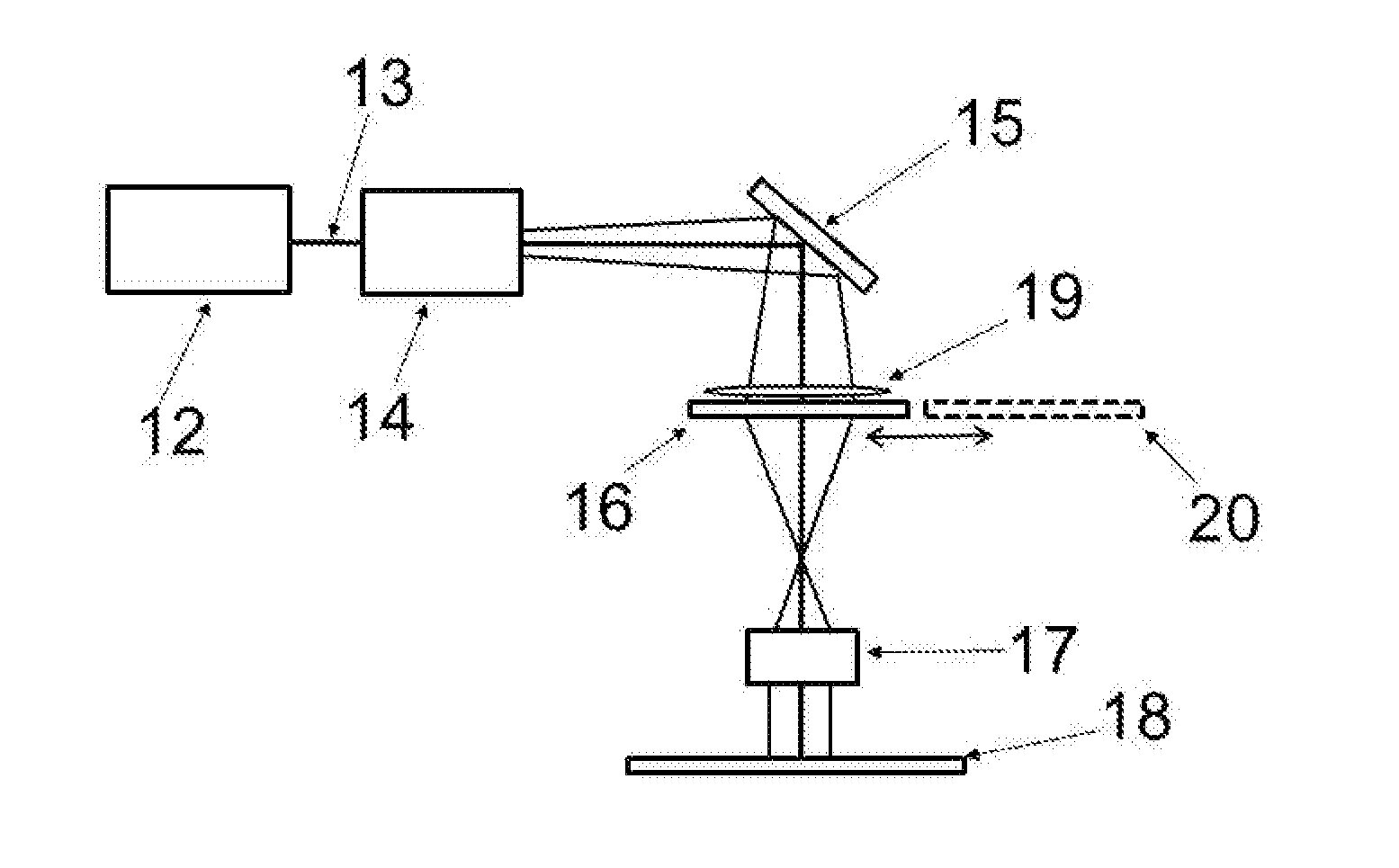
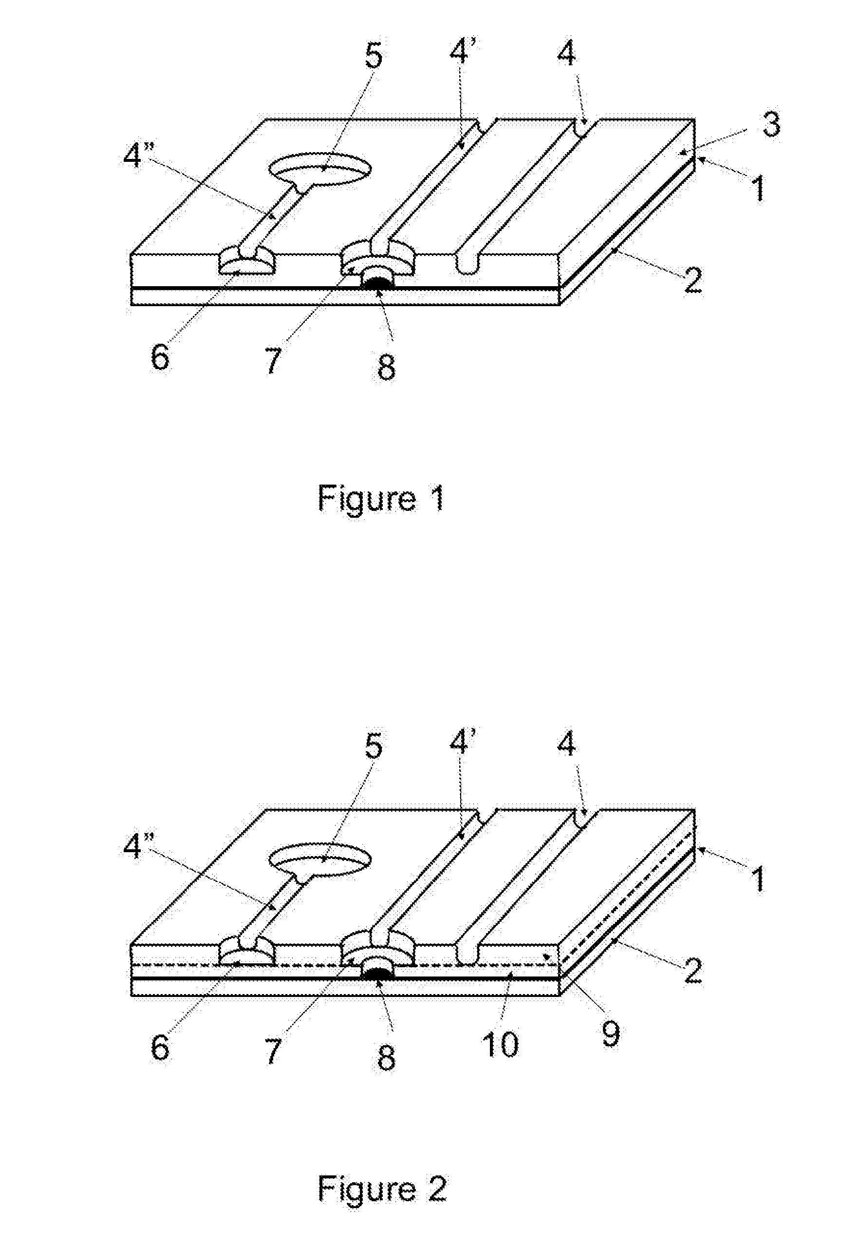
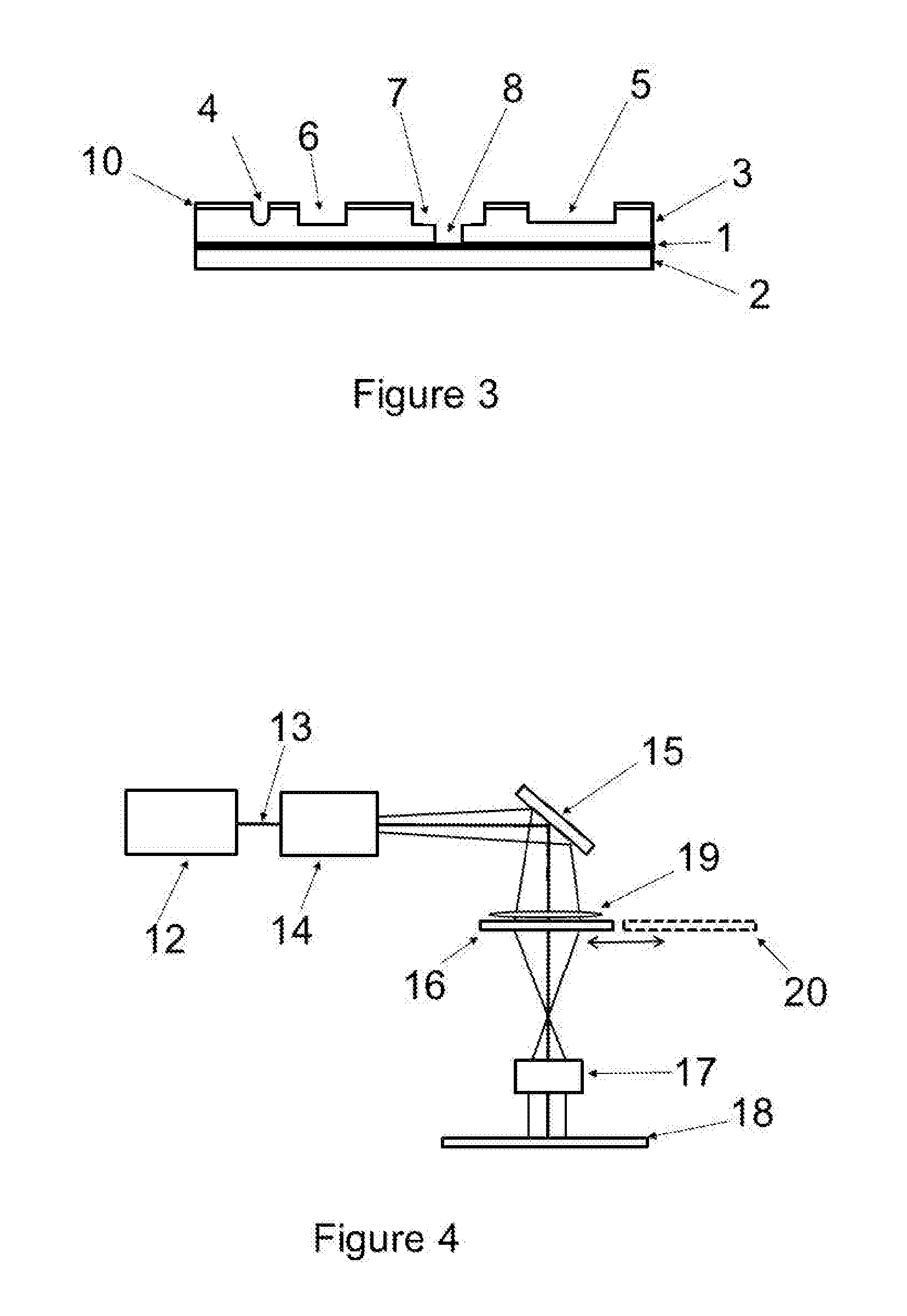
Drilling method for printed circuit board by laser beam
PatentInactiveJP1996323488A
Innovation
- A two-stage drilling process using a high-intensity pulsed laser beam or carbon dioxide gas laser beam (9.0 to 11.0 μm) followed by an excimer laser beam to remove residual resin layers, ensuring precise and efficient hole creation.
Method and apparatus for forming fine scale structures in dielectric substrate
PatentActiveUS20150230341A1
Innovation
- A two-stage process using a solid state laser with a mask projection system for forming structures at different depths, where a first set of structures is created using a Q-switched CW diode pumped solid state laser in a 2D raster scan, and a second set is formed using either the same or a different laser with optimized parameters, allowing for flexible and cost-effective production of embedded conductor layers.

Environmental Impact and Sustainability in PCB Manufacturing
The environmental implications of optimizing laser drilling techniques for substrate-like PCBs represent a critical consideration in modern electronics manufacturing. Traditional mechanical drilling methods generate significant material waste through chip formation and require extensive use of cutting fluids, which pose disposal challenges and potential groundwater contamination risks. Laser drilling optimization addresses these concerns by eliminating the need for chemical coolants and reducing material waste through precise, controlled ablation processes.
Energy consumption patterns in laser drilling systems have evolved significantly with technological advancement. Modern femtosecond and picosecond laser systems, while initially requiring higher peak power, demonstrate superior energy efficiency per drilled hole compared to conventional drilling methods. The elimination of tool wear and replacement cycles further reduces the overall environmental footprint, as carbide drill bits and their associated manufacturing processes contribute substantially to carbon emissions throughout their lifecycle.
Chemical usage reduction represents another significant environmental benefit of optimized laser drilling. Traditional PCB drilling requires extensive use of desmear chemicals, etchants, and cleaning solvents to prepare hole walls for plating processes. Advanced laser drilling techniques, particularly those employing ultrashort pulse lasers, create cleaner hole walls with minimal thermal damage, reducing the need for aggressive chemical treatments and associated waste streams.
Waste stream management in laser-optimized PCB manufacturing shows marked improvement over conventional methods. The absence of physical drill bits eliminates metal waste, while precise laser control minimizes substrate material removal, reducing overall solid waste generation. Additionally, the elimination of cutting fluid systems removes a significant source of hazardous liquid waste that requires specialized treatment and disposal protocols.
Carbon footprint analysis reveals that optimized laser drilling systems, despite higher initial energy requirements, demonstrate lower lifetime emissions when considering reduced consumable usage, elimination of tool transportation, and decreased chemical processing requirements. The integration of renewable energy sources with laser drilling systems further enhances sustainability profiles, making this technology increasingly attractive for environmentally conscious manufacturers seeking to meet stringent sustainability targets while maintaining production efficiency and quality standards.
Quality Standards and Testing Methods for Laser Drilled PCBs
Quality standards for laser drilled PCBs encompass multiple dimensional and performance criteria that ensure manufacturing consistency and reliability. The primary geometric specifications include hole diameter tolerance typically maintained within ±5-10 micrometers, positional accuracy requirements of ±12.5 micrometers, and circularity standards demanding deviation less than 2 micrometers. Wall surface roughness parameters must not exceed Ra 0.8 micrometers to prevent signal integrity degradation in high-frequency applications.
Electrical performance standards focus on impedance control and signal transmission characteristics. Controlled impedance tolerance for laser drilled vias typically ranges within ±10% of target values, while insertion loss specifications vary based on frequency requirements, generally not exceeding 0.1 dB per via at 10 GHz. Return loss parameters must maintain values below -20 dB across operational frequency ranges to ensure acceptable signal quality.
Testing methodologies employ both destructive and non-destructive evaluation techniques to validate drilling quality. Optical inspection systems utilize high-resolution cameras and automated measurement algorithms to assess hole geometry, detecting deviations in diameter, position, and shape. Cross-sectional analysis through microsectioning reveals internal wall quality, resin smear presence, and thermal damage extent around drill sites.
Electrical testing protocols include time domain reflectometry measurements to evaluate impedance consistency and identify discontinuities within drilled structures. Vector network analyzer testing quantifies insertion and return loss characteristics across specified frequency ranges. Continuity testing verifies proper electrical connections while isolation testing confirms adequate separation between adjacent conductors.
Advanced characterization methods incorporate scanning electron microscopy for detailed wall surface analysis and energy-dispersive X-ray spectroscopy to identify material composition changes induced by laser processing. Thermal cycling tests evaluate via reliability under temperature stress, while mechanical pull tests assess adhesion strength between plated copper and substrate materials.
Statistical process control implementation requires establishing control charts for critical parameters including hole diameter distribution, positional accuracy trends, and electrical performance metrics. Capability studies determine process stability and identify optimization opportunities for laser parameter adjustments. Regular calibration of measurement equipment ensures testing accuracy and traceability to international standards.
Unlock deeper insights with Patsnap Eureka Quick Research — get a full tech report to explore trends and direct your research. Try now!
Generate Your Research Report Instantly with AI Agent
Supercharge your innovation with Patsnap Eureka AI Agent Platform!