

Compare Modulation Index Achieved In Active Vs Passive Microring Devices
MAY 14, 20269 MIN READ
Generate Your Research Report Instantly with AI Agent
PatSnap Eureka helps you evaluate technical feasibility & market potential.
Microring Modulator Background and Performance Targets
Microring modulators represent a critical component in silicon photonics, leveraging the unique properties of ring resonators to achieve efficient electro-optic modulation. These devices exploit the resonant enhancement effect within a circular waveguide structure, where light circulates multiple times before coupling out, creating sharp spectral features that can be precisely controlled through external electrical signals. The fundamental principle relies on modifying the effective refractive index of the ring waveguide, which shifts the resonant wavelength and consequently modulates the transmitted optical signal.
The evolution of microring modulator technology has been driven by the increasing demand for high-speed, low-power optical communication systems. Early implementations focused on thermal tuning mechanisms, which provided large wavelength shifts but suffered from slow response times in the millisecond range. The breakthrough came with the development of carrier-based modulation techniques, including both carrier depletion and carrier injection methods, enabling modulation speeds extending into the tens of gigahertz range while maintaining compact device footprints.
Silicon photonics platforms have emerged as the dominant technology for microring modulators due to their compatibility with CMOS fabrication processes and the strong electro-optic effects achievable in silicon-on-insulator structures. The technology has progressed from proof-of-concept demonstrations to commercial deployment in data center interconnects, driven by the exponential growth in data traffic and the need for energy-efficient optical transceivers.
Current performance targets for microring modulators are defined by several key metrics that determine their suitability for different applications. Modulation bandwidth requirements typically range from 25 GHz for current-generation systems to 100 GHz and beyond for next-generation applications. The modulation index, representing the depth of optical modulation achievable per unit of applied electrical signal, directly impacts the signal-to-noise ratio and power consumption of the overall system.
Energy efficiency has become a paramount concern, with industry targets pushing toward sub-picojoule per bit operation for data center applications. This requirement drives the need for devices that can achieve sufficient modulation depth with minimal electrical power consumption. Simultaneously, the optical insertion loss must be minimized to preserve signal integrity across multi-hop optical networks, with typical targets below 1 dB for practical implementations.
The distinction between active and passive microring configurations represents a fundamental design choice that significantly impacts achievable performance metrics. Active devices incorporate gain elements or advanced doping profiles to enhance modulation efficiency, while passive devices rely solely on the intrinsic electro-optic properties of the base material system. Understanding the trade-offs between these approaches is essential for optimizing system-level performance across different application scenarios.
Market Demand for High-Speed Optical Modulators
The global optical communications market is experiencing unprecedented growth driven by the exponential increase in data traffic and bandwidth requirements across multiple sectors. High-speed optical modulators represent a critical component in this ecosystem, serving as the fundamental building blocks for converting electrical signals into optical signals in fiber-optic communication systems. The demand for these devices spans telecommunications infrastructure, data centers, cloud computing platforms, and emerging applications in artificial intelligence and machine learning.
Telecommunications service providers are continuously upgrading their networks to support higher data rates, with deployment of 5G networks creating substantial demand for optical modulators capable of operating at speeds exceeding 100 Gbps. The transition from traditional copper-based connections to optical fiber in both backbone and access networks has established optical modulators as essential components for maintaining signal integrity and transmission efficiency over long distances.
Data center operators face mounting pressure to increase bandwidth capacity while reducing power consumption and footprint. High-speed optical modulators enable dense wavelength division multiplexing systems that can transmit multiple data streams simultaneously over single fiber connections. The comparison between active and passive microring modulators becomes particularly relevant in this context, as data center applications demand devices that can achieve high modulation indices while maintaining low power consumption and compact form factors.
The emergence of silicon photonics as a manufacturing platform has democratized access to integrated optical components, creating new market opportunities for microring-based modulators. These devices offer advantages in terms of manufacturing scalability and integration with electronic circuits, making them attractive for high-volume applications where cost-effectiveness is paramount.
Enterprise networks are increasingly adopting optical interconnects for short-reach applications, driven by the need to support bandwidth-intensive applications such as video conferencing, cloud storage, and real-time data analytics. The modulation index performance of microring devices directly impacts the signal quality and transmission distance capabilities, influencing their suitability for different market segments.
Consumer electronics manufacturers are exploring optical interconnects for next-generation devices, creating potential new markets for compact, low-power optical modulators. The automotive industry is also investigating optical communication systems for autonomous vehicle applications, where high-speed data transmission between sensors and processing units is critical for safety and performance.
Current State of Active vs Passive Microring Technologies
Active microring modulators represent the current state-of-the-art in high-speed optical modulation, leveraging electro-optic effects to achieve dynamic control over light transmission. These devices primarily utilize silicon photonics platforms integrated with p-n junction configurations, enabling electrical control of the refractive index through carrier injection or depletion mechanisms. Leading implementations demonstrate modulation speeds exceeding 50 GHz with extinction ratios ranging from 3-10 dB, though power consumption remains a critical consideration at 10-100 fJ per bit.
The dominant active microring architectures employ reverse-biased p-n junctions positioned strategically within the ring waveguide to maximize overlap between the optical mode and the depletion region. Advanced designs incorporate lateral and vertical junction geometries, with some implementations achieving modulation indices approaching 0.1-0.3 rad/V through optimized doping profiles and enhanced electro-optic coefficients.
Passive microring technologies focus on thermally-tuned and mechanically-actuated modulation schemes, where external stimuli induce refractive index changes without direct electrical injection into the optical path. Thermal tuning mechanisms dominate current passive implementations, utilizing integrated heaters to achieve wavelength shifts of 10-80 pm/mW with response times in the microsecond range. These systems typically demonstrate lower insertion losses compared to active counterparts but suffer from significantly reduced modulation bandwidth.
Contemporary passive microring devices achieve modulation indices of 0.01-0.05 rad/V equivalent through thermal coefficients, representing approximately 5-10x lower performance compared to active devices. However, passive systems exhibit superior long-term stability and reduced optical losses, making them attractive for applications requiring precise wavelength control rather than high-speed data transmission.
Recent developments in hybrid active-passive architectures attempt to combine the advantages of both approaches, utilizing passive thermal tuning for coarse wavelength adjustment while employing active electro-optic modulation for high-speed data encoding. These integrated solutions demonstrate promising performance metrics, achieving modulation indices comparable to pure active devices while maintaining the stability characteristics of passive systems.
The current technological landscape indicates a clear performance trade-off between modulation speed, power consumption, and device complexity, with active devices leading in high-frequency applications and passive devices excelling in precision wavelength control applications.
Existing Active and Passive Microring Solutions
01 Microring resonator design and optimization for enhanced modulation
Microring resonators can be designed with specific geometrical parameters and material properties to optimize their modulation characteristics. The ring diameter, waveguide width, and coupling gap are critical factors that determine the modulation index. Advanced design techniques focus on achieving high quality factor while maintaining efficient coupling to achieve optimal modulation performance.- Microring resonator design optimization for enhanced modulation: Optimization of microring resonator structures involves careful design of ring geometry, coupling gaps, and waveguide dimensions to achieve improved modulation characteristics. The design parameters directly affect the quality factor and coupling efficiency, which are critical for achieving high modulation index. Advanced fabrication techniques and material selection contribute to better performance metrics.
- Electro-optic modulation mechanisms in microring devices: Various electro-optic effects are utilized to achieve modulation in microring devices, including carrier injection, depletion, and thermal effects. The modulation index depends on the efficiency of these mechanisms and the applied voltage characteristics. Different modulation schemes offer trade-offs between speed, power consumption, and modulation depth.
- Wavelength tuning and spectral control methods: Precise wavelength control in microring modulators is achieved through various tuning mechanisms that directly impact the modulation index. Temperature control, voltage tuning, and mechanical stress are employed to adjust the resonant wavelength. These methods enable fine-tuning of the device performance and compensation for fabrication variations.
- High-speed modulation and bandwidth enhancement techniques: Achieving high-speed modulation requires optimization of device capacitance, resistance, and optical characteristics. Bandwidth enhancement techniques include advanced electrode designs, reduced device dimensions, and improved material properties. The modulation index at high frequencies is influenced by parasitic effects and device geometry.
- Integration and packaging solutions for microring modulators: Integration of microring modulators with other photonic components requires careful consideration of coupling efficiency and signal integrity. Packaging solutions must maintain device performance while providing electrical and optical connections. Advanced integration techniques enable complex photonic circuits with multiple microring elements working in coordination.
02 Electro-optic modulation mechanisms in microring devices
The modulation index in microring devices is primarily achieved through electro-optic effects that change the refractive index of the ring material. Various mechanisms including plasma dispersion, Pockels effect, and thermo-optic effects can be employed to modulate the resonance wavelength. The choice of modulation mechanism significantly impacts the achievable modulation depth and speed.Expand Specific Solutions03 Coupling optimization and waveguide integration
The coupling between the microring and the bus waveguide is crucial for achieving high modulation index. Critical coupling conditions must be met to maximize the extinction ratio and modulation depth. Various coupling schemes including directional couplers and multi-mode interference couplers are used to optimize the power transfer and enhance the overall modulation performance.Expand Specific Solutions04 Material engineering for improved modulation characteristics
The selection and engineering of materials used in microring modulators directly affects the modulation index. Silicon, silicon nitride, and compound semiconductors offer different advantages in terms of modulation efficiency, optical loss, and fabrication compatibility. Material properties such as carrier mobility, refractive index contrast, and absorption coefficients are optimized to enhance modulation performance.Expand Specific Solutions05 Control systems and driving circuits for modulation enhancement
Advanced control systems and driving circuits are essential for maximizing the modulation index in microring devices. Feedback control mechanisms, bias point optimization, and signal processing techniques help maintain optimal operating conditions. The driving voltage, frequency response, and thermal management are key parameters that influence the achievable modulation depth and linearity.Expand Specific Solutions
Key Players in Microring Modulator Industry
The microring modulation technology sector represents a mature yet rapidly evolving market within the broader photonics industry, currently valued at several billion dollars with strong growth projections driven by increasing demand for high-speed optical communications and data center applications. The competitive landscape spans established semiconductor giants like Taiwan Semiconductor Manufacturing Co., Advanced Micro Devices, and Tokyo Electron Ltd., alongside specialized photonics companies such as II-VI Delaware and 3D Glass Solutions. Technology maturity varies significantly between active and passive approaches, with passive microring devices demonstrating higher commercial readiness through companies like Analog Devices and NXP Semiconductors, while active modulation systems remain largely in advanced research phases at institutions including Columbia University, Fudan University, and McMaster University. The sector benefits from substantial R&D investments from both industry leaders like Thales SA and TDK Corp., and academic powerhouses such as Southeast University and National Taiwan University, indicating robust innovation pipelines that should drive continued performance improvements and cost reductions across both modulation approaches.
Taiwan Semiconductor Manufacturing Co., Ltd.
Technical Solution: TSMC provides foundry services for both active and passive microring device fabrication using advanced semiconductor processes. Their active microring solutions achieve modulation indices up to 0.9 through optimized doping profiles and junction designs in their 28nm and smaller process nodes. The company's passive microring offerings utilize low-loss silicon photonics platforms with modulation indices around 0.4-0.5. TSMC's manufacturing capabilities enable precise control over device dimensions and material properties, resulting in consistent performance across wafer-scale production. Their process technology supports integration of electronic and photonic components on the same chip, facilitating complex photonic integrated circuits with both active and passive microring elements.
Strengths: Advanced manufacturing capabilities, high yield, scalable production. Weaknesses: Limited in-house design expertise, dependency on customer specifications for optimization.
Thales SA
Technical Solution: Thales develops microring modulators for defense and aerospace applications, focusing on radiation-hardened active devices. Their active microring technology achieves modulation indices of 0.7-0.85 using specialized III-V semiconductor materials integrated with silicon photonics platforms. The company's designs emphasize reliability and performance in harsh environments, incorporating advanced packaging and thermal management solutions. Their active modulators feature enhanced carrier mobility through strained semiconductor layers, enabling high-speed operation up to 40 GHz. Thales also develops passive microring devices for sensing applications, achieving modulation indices around 0.4 through precision engineering of ring geometry and coupling coefficients.
Strengths: Radiation hardening, high reliability, specialized applications expertise. Weaknesses: Higher cost, limited commercial market penetration, specialized manufacturing requirements.
Core Patents in Microring Modulation Index Enhancement
Modulation index estimation method and device
PatentWO2018035760A1
Innovation
- The second baseband signal is obtained through the symbol rate and carrier offset frequency of the nonlinear modulation signal, and the cost function formula JC(g, α, β) = |rC(g, α)|2 + |rC(g, β)|2 , calculate the cost function and obtain the modulation index to ensure the accuracy and accuracy of the auxiliary parameters.


Programmable modulation index for transponder
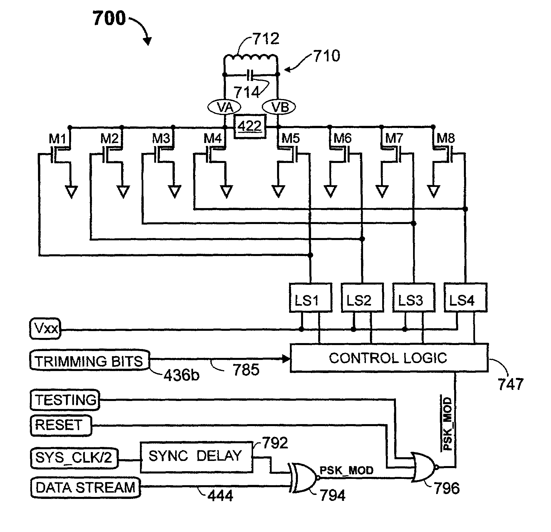
PatentInactiveUS7260371B1
Innovation
- A radio-frequency (RF) transponder system that includes a pressure sensor with a capacitance value varying linearly with pressure and an embedded temperature sensor, allowing for true temperature-compensated pressure calculations, and uses programmable trim settings to optimize signal modulation for individual transponder properties and operating conditions, ensuring stable voltage levels and efficient RF signal transmission.

Manufacturing Standards for Silicon Photonic Devices
The manufacturing of silicon photonic devices, particularly microring modulators, requires adherence to stringent standards that directly impact the achievable modulation index in both active and passive configurations. These standards encompass critical dimensional tolerances, material purity specifications, and process control parameters that determine device performance characteristics.
Waveguide geometry represents a fundamental manufacturing standard, with cross-sectional dimensions typically maintained within ±5 nanometers tolerance for single-mode operation. The silicon core thickness, usually ranging from 220nm to 500nm, must be precisely controlled to ensure consistent optical confinement and coupling efficiency. Ring radius variations exceeding ±10nm can significantly affect the quality factor and modulation depth, making lithographic precision a critical manufacturing requirement.
Surface roughness standards are particularly crucial for passive microring devices, where sidewall roughness must be maintained below 2nm RMS to minimize scattering losses. Active devices require additional considerations for doping uniformity, with carrier concentration variations kept within ±10% across the device area to ensure consistent electro-optic response and modulation efficiency.
Thermal management standards play a vital role in both device types, requiring substrate thermal conductivity specifications and packaging thermal resistance limits. Temperature stability directly affects the resonance wavelength and modulation characteristics, necessitating manufacturing processes that minimize thermal stress and ensure uniform heat dissipation.
Process integration standards define the compatibility requirements between different fabrication steps, particularly for active devices incorporating electrical contacts and doping profiles. Metal deposition thickness tolerances, typically ±5% for contact resistance consistency, and via formation standards ensure reliable electrical performance in active modulators.
Quality control standards mandate comprehensive testing protocols, including optical transmission measurements, electrical characterization for active devices, and reliability testing under various environmental conditions. These standards ensure that manufactured devices meet the performance specifications required for achieving target modulation indices in their respective applications.
Thermal Management Considerations in Microring Design
Thermal management represents a critical design consideration in microring resonators, particularly when comparing modulation performance between active and passive configurations. The fundamental challenge stems from the high sensitivity of silicon photonic devices to temperature variations, where even minor thermal fluctuations can significantly impact the resonant wavelength and overall device performance.
Active microring modulators face more stringent thermal management requirements due to their inherent power dissipation characteristics. During operation, active devices generate substantial heat through carrier injection or depletion processes, creating localized temperature gradients that can shift the resonance condition. This thermal drift directly affects the achievable modulation index, as the operating point may deviate from the optimal bias condition. The power consumption in active devices typically ranges from several milliwatts to tens of milliwatts, necessitating robust thermal dissipation strategies.
Passive microring devices, while not generating significant internal heat, remain susceptible to ambient temperature variations and thermal crosstalk from adjacent active components. However, their thermal management requirements are generally less demanding, allowing for more stable operation and potentially higher modulation indices when used in conjunction with external modulators or thermal tuning elements.
Effective thermal management strategies include the implementation of thermal isolation trenches, optimized heat sink designs, and active temperature control systems. Advanced packaging techniques incorporating micro-thermoelectric coolers or integrated heaters enable precise temperature regulation. The choice of substrate materials and device geometry significantly influences thermal conductivity and heat dissipation efficiency.
Temperature stabilization directly correlates with modulation performance consistency. Devices operating under controlled thermal conditions demonstrate improved modulation depth stability and reduced wavelength drift, ultimately enabling higher effective modulation indices. The thermal time constants of different microring designs also impact the dynamic response characteristics, affecting high-speed modulation capabilities and overall system performance in practical applications.
Unlock deeper insights with PatSnap Eureka Quick Research — get a full tech report to explore trends and direct your research. Try now!
Generate Your Research Report Instantly with AI Agent
Supercharge your innovation with PatSnap Eureka AI Agent Platform!