

Optimizing Electrical Biasing Schemes For Microring Modulators On Chips
MAY 14, 20268 MIN READ
Generate Your Research Report Instantly with AI Agent
PatSnap Eureka helps you evaluate technical feasibility & market potential.
Microring Modulator Biasing Background and Objectives
Microring modulators represent a cornerstone technology in silicon photonics, enabling high-speed optical communication systems through efficient electro-optic modulation. These devices leverage the resonant properties of ring-shaped waveguides to achieve compact footprints while maintaining superior performance characteristics. The fundamental operating principle relies on the plasma dispersion effect in silicon, where applied electrical bias modulates the refractive index, thereby shifting the resonant wavelength and controlling optical transmission.
The evolution of microring modulator technology has been driven by the exponential growth in data communication demands and the limitations of traditional electronic interconnects. Early developments focused on basic ring resonator structures, but modern implementations incorporate sophisticated designs including coupled-ring configurations, multi-ring cascades, and hybrid integration approaches. The progression from proof-of-concept demonstrations to commercial deployment has highlighted the critical importance of precise electrical biasing control for optimal device performance.
Current technological objectives center on achieving unprecedented levels of modulation efficiency while minimizing power consumption and thermal sensitivity. The primary goal involves developing adaptive biasing schemes that can dynamically compensate for process variations, temperature fluctuations, and aging effects that traditionally degrade device performance. These variations can cause significant wavelength drift, leading to reduced extinction ratios and increased insertion losses.
Advanced biasing optimization aims to implement intelligent control algorithms capable of real-time performance monitoring and automatic adjustment. This includes developing feedback mechanisms that utilize integrated photodetectors to continuously assess modulation quality and adjust bias voltages accordingly. The integration of machine learning algorithms for predictive bias control represents a frontier objective, enabling proactive compensation before performance degradation occurs.
Furthermore, the development of standardized biasing protocols for large-scale photonic integrated circuits constitutes a critical objective. As chip-scale optical systems incorporate hundreds or thousands of microring modulators, coordinated biasing strategies become essential for maintaining system-level performance while managing power budgets and thermal management constraints.
Market Demand for High-Performance Optical Modulators
The global optical communications market is experiencing unprecedented growth driven by the exponential increase in data traffic and bandwidth requirements across multiple sectors. Data centers, telecommunications networks, and high-performance computing systems are demanding increasingly sophisticated optical interconnect solutions to handle massive data volumes with minimal latency and power consumption. This surge in demand directly translates to heightened requirements for high-performance optical modulators, particularly silicon photonic devices that can be integrated with electronic circuits on the same chip.
Microring modulators have emerged as critical components in meeting these market demands due to their compact footprint, low power consumption, and compatibility with CMOS fabrication processes. The telecommunications industry's transition toward 5G networks and beyond requires optical modulators capable of operating at higher frequencies with improved signal integrity. Similarly, the rapid expansion of cloud computing services and artificial intelligence applications necessitates optical interconnects that can support terabit-scale data transmission rates while maintaining energy efficiency.
The market demand for optimized electrical biasing schemes specifically stems from the need to enhance modulator performance metrics that directly impact system-level capabilities. Network operators and data center providers are increasingly focused on reducing operational expenses through improved power efficiency and enhanced signal quality. Proper electrical biasing optimization enables microring modulators to achieve better extinction ratios, reduced insertion losses, and improved thermal stability, all of which contribute to overall system performance and reliability.
Enterprise customers are particularly interested in solutions that can deliver consistent performance across varying environmental conditions while minimizing maintenance requirements. The ability to dynamically adjust biasing schemes to compensate for temperature fluctuations and process variations represents a significant value proposition in commercial deployments. This demand is further amplified by the growing adoption of coherent optical communication systems that require precise control over modulator characteristics.
The automotive industry's evolution toward autonomous vehicles and the proliferation of Internet of Things devices are creating additional market segments that require robust, high-performance optical communication solutions. These applications demand modulators with enhanced reliability and performance consistency, making optimized electrical biasing schemes increasingly valuable for manufacturers seeking to address these emerging market opportunities.
Current Biasing Challenges in Silicon Photonics
Silicon photonic microring modulators face significant electrical biasing challenges that fundamentally limit their performance and commercial viability. The primary challenge stems from the inherent thermal sensitivity of silicon-based devices, where temperature fluctuations cause wavelength drift that disrupts the precise resonance conditions required for optimal modulation efficiency. This thermal instability necessitates continuous bias adjustment to maintain device performance across varying operating conditions.
Process variations during fabrication introduce substantial device-to-device inconsistencies in resonance wavelengths and quality factors. These variations can span several nanometers, requiring individual calibration and compensation schemes for each device on a chip. The lack of manufacturing uniformity complicates the implementation of standardized biasing protocols and increases system complexity.
Power consumption represents another critical constraint, as traditional thermal tuning methods consume significant electrical power to achieve wavelength alignment. The power requirements scale poorly with device count, making large-scale integration economically unfeasible. Additionally, the slow thermal response time limits the dynamic range of bias adjustments, preventing rapid adaptation to changing operating conditions.
Voltage-induced carrier effects in silicon create nonlinear responses that complicate precise bias control. The plasma dispersion effect, while enabling electro-optic modulation, introduces coupling between the bias voltage and both refractive index and absorption changes. This coupling creates interdependencies that make independent control of different device parameters challenging.
Cross-talk between adjacent devices on dense photonic integrated circuits presents additional biasing complications. Electrical and thermal coupling between neighboring components can cause unintended bias drift and performance degradation. The proximity effects become more pronounced as device density increases, limiting the scalability of current biasing approaches.
Long-term stability issues plague existing biasing schemes, as aging effects and environmental stress gradually shift device characteristics. The temporal drift requires continuous monitoring and adjustment, adding complexity to control systems and reducing overall reliability. These stability challenges are particularly problematic for applications requiring consistent performance over extended operational periods.
Existing Electrical Biasing Solutions for Microring Devices
01 Voltage control and bias optimization techniques
Various electrical biasing schemes focus on optimizing voltage control methods to enhance microring modulator performance. These techniques involve precise voltage regulation, bias point stabilization, and adaptive control mechanisms to maintain optimal operating conditions. The schemes typically incorporate feedback systems and voltage adjustment algorithms to compensate for temperature variations and process fluctuations.- Voltage control and bias optimization techniques: Various electrical biasing schemes focus on optimizing voltage control methods to enhance microring modulator performance. These techniques involve precise voltage regulation, bias point stabilization, and adaptive control mechanisms to maintain optimal operating conditions. The schemes typically incorporate feedback systems and voltage reference circuits to ensure stable modulation characteristics across different operating conditions.
- Thermal compensation and bias stabilization: Electrical biasing schemes that address temperature-induced variations in microring modulators through thermal compensation mechanisms. These approaches utilize temperature sensing circuits, thermal feedback loops, and adaptive bias adjustment systems to maintain consistent performance despite environmental temperature changes. The stabilization methods help preserve modulation efficiency and prevent thermal drift effects.
- Multi-electrode biasing configurations: Advanced biasing schemes employing multiple electrode arrangements to achieve enhanced control over microring modulator characteristics. These configurations enable independent control of different modulator parameters through segmented electrodes, differential biasing, and multi-point electrical contacts. Such schemes provide improved modulation bandwidth and better linearity control.
- Power management and efficiency optimization: Electrical biasing approaches focused on minimizing power consumption while maintaining high modulation performance. These schemes incorporate low-power bias circuits, energy-efficient driving methods, and power-aware control algorithms. The optimization techniques balance performance requirements with power constraints in integrated photonic systems.
- Integrated control and monitoring systems: Comprehensive electrical biasing schemes that integrate control and monitoring functionalities for microring modulators. These systems combine bias control circuits with performance monitoring capabilities, automatic calibration features, and real-time adjustment mechanisms. The integrated approach enables autonomous operation and maintains optimal modulator performance through continuous feedback and adjustment.
02 Thermal compensation and stabilization methods
Electrical biasing approaches that address thermal effects in microring modulators through compensation circuits and stabilization techniques. These methods involve temperature sensing, thermal drift correction, and active thermal management to maintain consistent modulation characteristics across varying operating conditions. The schemes often integrate heating elements or cooling mechanisms with electrical control systems.Expand Specific Solutions03 Multi-electrode and differential biasing configurations
Advanced biasing schemes utilizing multiple electrodes and differential voltage applications to achieve enhanced control over microring modulator characteristics. These configurations enable independent control of different modulation parameters and provide improved linearity and bandwidth performance. The approaches often involve segmented electrode designs and sophisticated driving circuits.Expand Specific Solutions04 High-speed switching and modulation control
Electrical biasing techniques specifically designed for high-frequency operation and rapid switching applications in microring modulators. These schemes focus on minimizing switching time, reducing power consumption, and maintaining signal integrity at high data rates. The methods typically involve optimized driver circuits, impedance matching, and signal conditioning approaches.Expand Specific Solutions05 Integrated control circuits and feedback systems
Comprehensive electrical biasing solutions that incorporate on-chip control circuits, monitoring systems, and closed-loop feedback mechanisms for microring modulators. These integrated approaches provide real-time performance optimization, automatic bias adjustment, and system-level control capabilities. The schemes often include digital signal processing elements and adaptive algorithms for autonomous operation.Expand Specific Solutions
Key Players in Silicon Photonics and Modulator Industry
The microring modulator optimization field represents a rapidly evolving segment within the broader photonic integrated circuits market, currently in its growth phase with increasing demand for high-speed optical communications. The market demonstrates significant expansion potential, driven by data center modernization and 5G infrastructure deployment requirements. Technology maturity varies considerably across market participants, with established semiconductor giants like Intel Corp., Infineon Technologies AG, and STMicroelectronics leading advanced development efforts alongside specialized photonics companies such as Ciena Corp. and Mellanox Technologies Ltd. Research institutions including Fraunhofer-Gesellschaft, CEA, and various universities contribute fundamental innovations, while companies like MediaTek and ZTE Corp. focus on commercial applications. The competitive landscape shows a mix of mature players with proven fabrication capabilities and emerging specialists developing novel biasing schemes, indicating a dynamic market with substantial technological advancement opportunities and increasing commercial viability.
Intel Corp.
Technical Solution: Intel has developed advanced silicon photonics technology with integrated microring modulators featuring sophisticated electrical biasing schemes. Their approach utilizes reverse-biased p-n junctions in silicon microring resonators to achieve high-speed electro-optic modulation. The company implements multi-level biasing architectures that optimize both DC and RF performance, incorporating temperature compensation circuits and adaptive bias control systems. Intel's microring modulators achieve modulation speeds exceeding 25 Gbps with optimized power consumption through dynamic bias adjustment algorithms. Their biasing schemes include pre-emphasis and equalization techniques to enhance signal integrity across different operating conditions.
Strengths: Industry-leading fabrication capabilities and extensive silicon photonics expertise. Weaknesses: High development costs and complex integration requirements for advanced biasing circuits.
Ciena Corp.
Technical Solution: Ciena has developed proprietary electrical biasing optimization techniques for microring modulators used in their coherent optical transmission systems. Their approach focuses on adaptive bias control algorithms that dynamically adjust operating points to maintain optimal extinction ratios and minimize power consumption. The company implements machine learning-based bias optimization that continuously monitors performance metrics and adjusts biasing parameters in real-time. Their microring modulator biasing schemes incorporate temperature drift compensation and aging compensation mechanisms to ensure long-term stability. Ciena's solutions achieve sub-microsecond bias adjustment response times while maintaining modulation bandwidths exceeding 32 GHz through optimized electrode designs and bias network topologies.
Strengths: Strong expertise in optical networking and real-time adaptive control systems. Weaknesses: Limited to specific application domains and requires sophisticated control electronics.
Core Patents in Microring Modulator Biasing Optimization
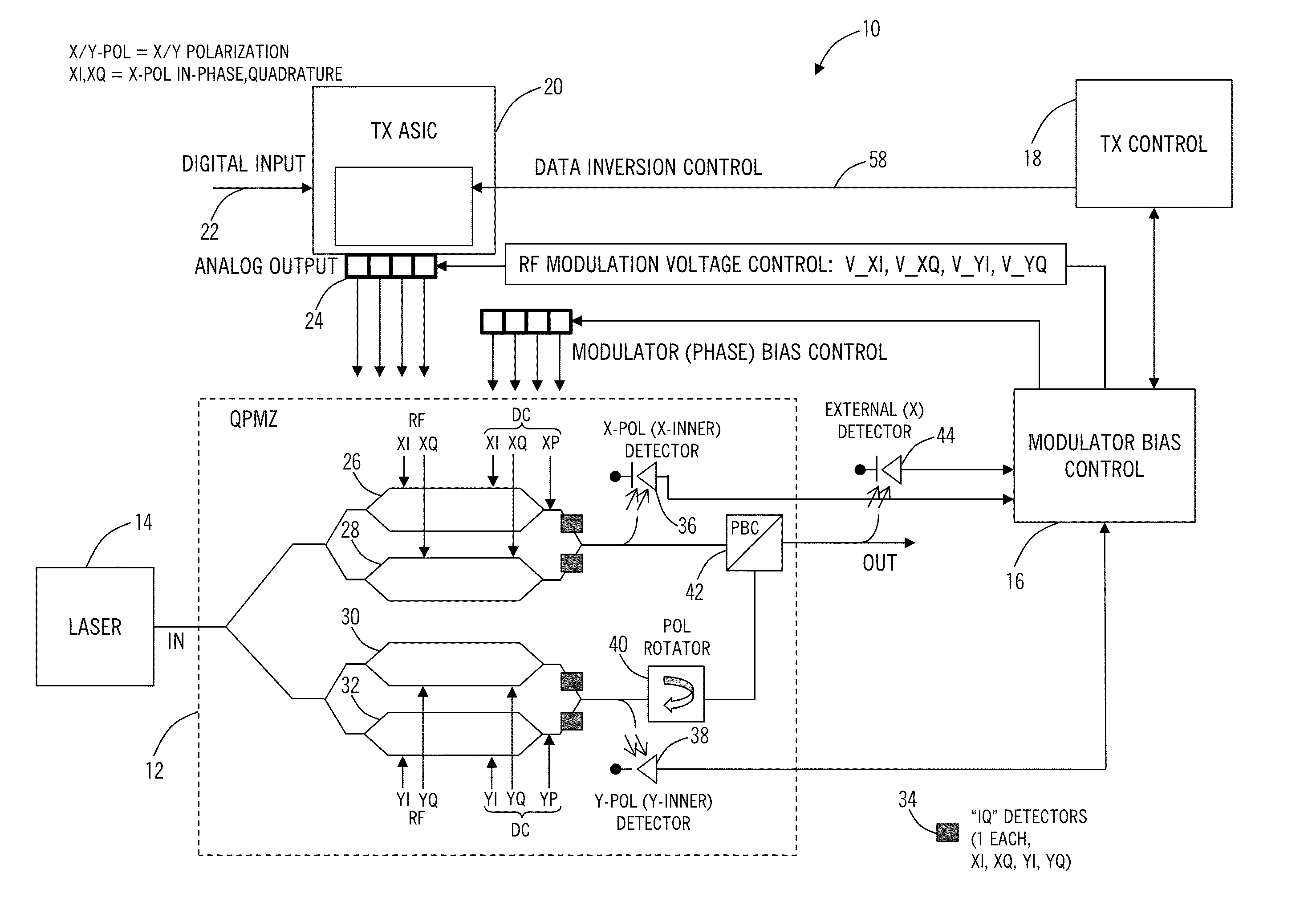
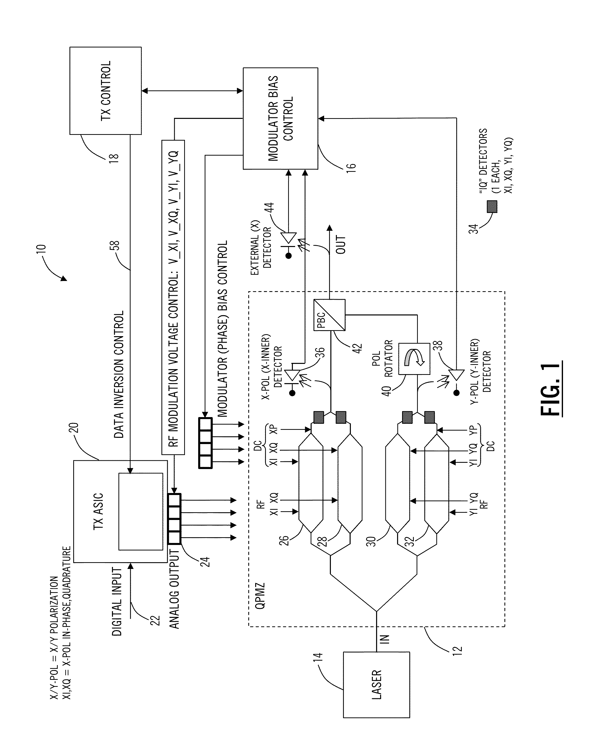
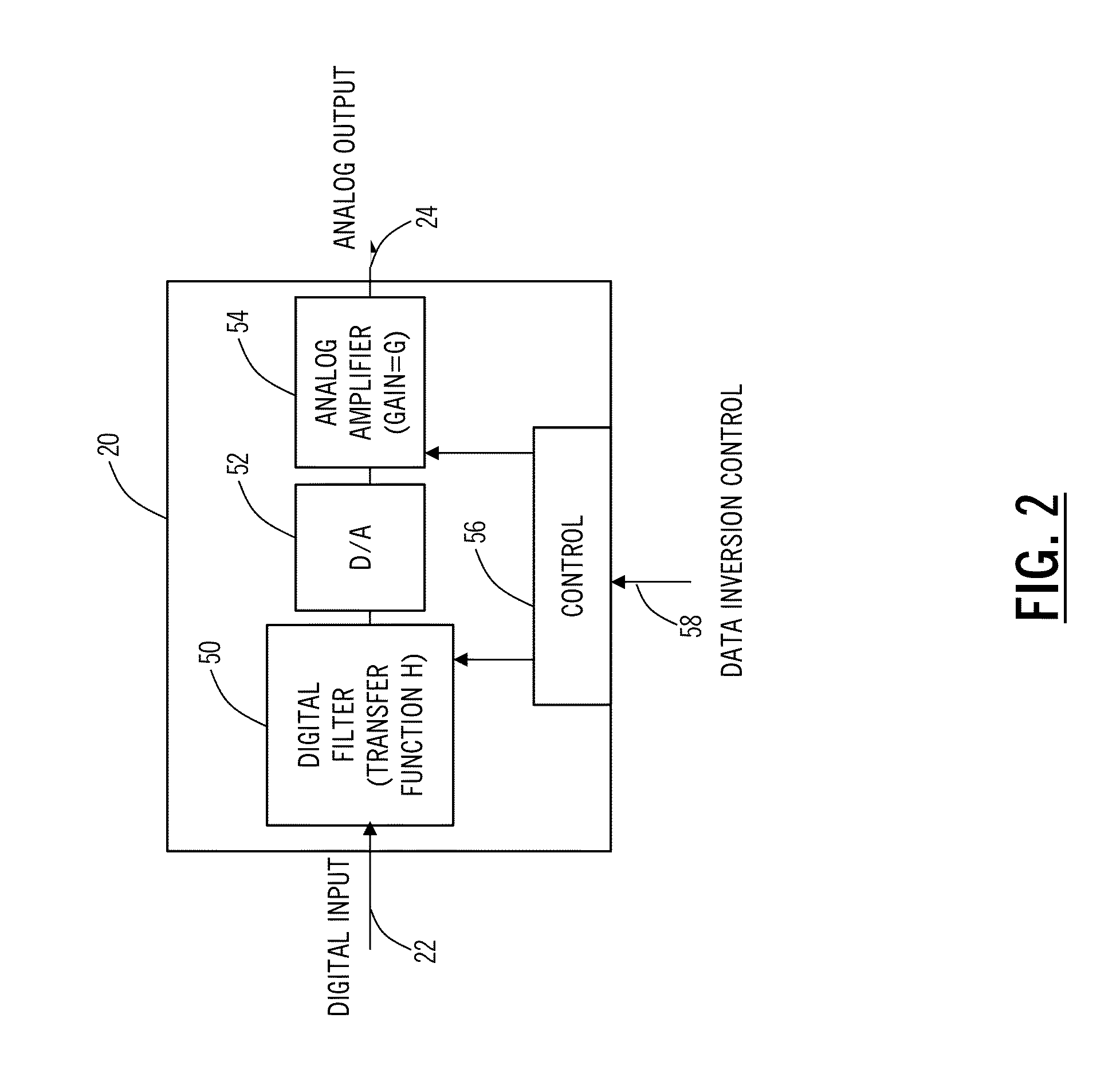
Optimum modulator bias systems and methods in coherent optical transmitters
PatentActiveUS20140308047A1
Innovation
- A method for selecting minimum and half-power bias points for optical modulators using a local algorithm that sweeps phase adjusters to find optimal settings, employing detectors to determine these points efficiently, and applying data inversion for desired constellations, allowing for optimal phase control with minimal phase adjustment.

Technologies for programmable microring resonators
PatentPendingUS20250306427A1
Innovation
- A semiconductor junction in the microring modulator is forward biased to control the coupling regime by adjusting the charge density, reducing the quality factor, and shifting the microring modulator towards an undercoupled regime, allowing for tuning of the coupling rate.


Thermal Management Considerations for Biasing Circuits
Thermal management represents a critical design consideration for biasing circuits in microring modulator systems, as temperature variations directly impact both the electrical performance and optical characteristics of these devices. The biasing circuits themselves generate heat through resistive losses and switching activities, while simultaneously being sensitive to temperature-induced parameter drift that can compromise modulation efficiency and signal integrity.
The primary thermal challenge stems from the interdependence between electrical biasing performance and temperature stability. As biasing circuits operate, power dissipation occurs through various mechanisms including DC bias current flow, dynamic switching losses in driver circuits, and leakage currents in semiconductor components. This heat generation creates localized temperature gradients that can shift the resonance wavelength of microring modulators, requiring continuous bias adjustments to maintain optimal operating points.
Temperature coefficient management becomes particularly crucial for bias voltage references and current sources within the biasing architecture. Standard silicon-based bias generation circuits exhibit temperature coefficients that can cause significant drift in output levels, directly translating to wavelength shifts in the optical domain. Advanced biasing schemes must incorporate temperature compensation techniques, such as bandgap voltage references and proportional-to-absolute-temperature current sources, to minimize thermal sensitivity.
Heat dissipation pathways require careful consideration during biasing circuit layout and packaging design. Effective thermal management strategies include strategic placement of heat-generating components away from temperature-sensitive elements, implementation of thermal vias and heat spreaders, and integration of active cooling solutions where necessary. The thermal resistance between biasing circuits and heat sinks must be minimized to prevent excessive junction temperatures that could degrade component reliability.
Dynamic thermal effects present additional challenges, particularly in high-speed modulation scenarios where rapid power variations create transient temperature fluctuations. These thermal transients can introduce unwanted frequency modulation and amplitude variations in the optical output. Biasing circuit designs must account for thermal time constants and implement appropriate filtering or compensation mechanisms to mitigate these effects while maintaining the required electrical bandwidth for modulation signals.
Power Efficiency Standards for Integrated Photonic Systems
Power efficiency standards for integrated photonic systems have become increasingly critical as the demand for high-performance optical communication and computing applications continues to grow. These standards establish benchmarks for energy consumption, thermal management, and overall system performance that directly impact the viability of microring modulator implementations in commercial applications.
The IEEE 802.3 Ethernet standards have established power consumption limits for optical transceivers, with recent amendments targeting sub-picojoule per bit energy efficiency for short-reach applications. These specifications drive the development of low-power electrical biasing schemes, as traditional voltage-controlled modulation approaches often exceed acceptable power budgets when scaled to multi-channel systems.
Industry consortiums such as the Optical Internetworking Forum and the Common Public Radio Interface have developed complementary standards focusing on thermal design power limits and power supply efficiency requirements. For silicon photonic platforms, the typical power budget allocation allows 10-50 milliwatts per optical channel, creating stringent constraints on bias circuit design and modulation voltage requirements.
Emerging standards from organizations like JEDEC and the International Electrotechnical Commission address power management protocols specifically for photonic integrated circuits. These include dynamic power scaling requirements, standby mode specifications, and power-on sequencing protocols that influence bias circuit architecture decisions for microring modulators.
The development of application-specific power efficiency metrics has gained momentum, particularly for data center interconnects and high-performance computing applications. These metrics consider not only static power consumption but also dynamic power scaling capabilities, modulation efficiency ratios, and thermal coupling effects between adjacent optical components.
Recent standardization efforts have focused on establishing measurement methodologies for power efficiency assessment, including standardized test conditions, temperature coefficients, and aging characteristics. These protocols ensure consistent evaluation of different electrical biasing approaches and enable fair comparison between competing technological solutions in the marketplace.
Unlock deeper insights with PatSnap Eureka Quick Research — get a full tech report to explore trends and direct your research. Try now!
Generate Your Research Report Instantly with AI Agent
Supercharge your innovation with PatSnap Eureka AI Agent Platform!