

Comparing Dielectric Materials Suitability For Electron Beam Processes
APR 28, 20269 MIN READ
Generate Your Research Report Instantly with AI Agent
PatSnap Eureka helps you evaluate technical feasibility & market potential.
Dielectric Materials for E-beam Processing Background and Objectives
Electron beam processing has emerged as a critical technology across multiple industrial sectors, fundamentally transforming manufacturing processes through precise material modification and fabrication capabilities. This advanced technique utilizes focused electron beams to interact with materials at the atomic level, enabling applications ranging from semiconductor device fabrication to advanced materials synthesis. The technology's significance has grown exponentially with the increasing demand for miniaturization and precision in modern electronics and nanotechnology applications.
The evolution of electron beam processing traces back to the early developments in electron microscopy and lithography in the mid-20th century. Initial applications focused primarily on imaging and basic material analysis. However, technological breakthroughs in beam control, vacuum systems, and computational modeling have expanded its utility to encompass complex manufacturing processes. Today's electron beam systems achieve unprecedented precision levels, with beam diameters reaching sub-nanometer scales and energy control spanning several orders of magnitude.
Central to the effectiveness of electron beam processing is the selection and optimization of dielectric materials that serve as substrates, masks, or protective layers during beam exposure. These materials must exhibit specific electrical, thermal, and mechanical properties to withstand the intense energy deposition while maintaining structural integrity and desired functionality. The interaction between high-energy electrons and dielectric materials involves complex physical phenomena including secondary electron emission, charge accumulation, thermal dissipation, and potential chemical modifications.
Current technological objectives focus on developing comprehensive frameworks for evaluating dielectric material suitability across diverse electron beam applications. This involves establishing standardized testing protocols, predictive modeling capabilities, and material selection criteria that account for beam energy, exposure duration, environmental conditions, and desired outcomes. The goal extends beyond simple material compatibility to encompass optimization strategies that maximize processing efficiency while minimizing unwanted side effects such as charging, thermal damage, or structural degradation.
The strategic importance of this research area continues to intensify as industries push toward more sophisticated electron beam applications. Emerging fields such as quantum device fabrication, advanced packaging technologies, and next-generation semiconductor architectures demand increasingly precise material engineering solutions. Understanding the fundamental relationships between dielectric properties and electron beam interactions represents a cornerstone for unlocking these advanced manufacturing capabilities and maintaining competitive advantages in technology-driven markets.
Market Demand Analysis for E-beam Compatible Dielectric Materials
The semiconductor manufacturing industry represents the primary driver for e-beam compatible dielectric materials demand, with advanced lithography processes requiring increasingly sophisticated material solutions. As device geometries continue shrinking below 7nm nodes, traditional photolithography faces fundamental limitations, creating substantial market opportunities for electron beam lithography systems and their associated dielectric materials. The transition toward extreme ultraviolet and electron beam processes has intensified requirements for dielectrics that maintain structural integrity under high-energy electron bombardment while preserving electrical properties.
Emerging applications in quantum computing and neuromorphic devices are generating new demand segments for specialized dielectric materials. These next-generation technologies require ultra-low loss dielectrics capable of withstanding electron beam processing without degradation of quantum coherence properties or synaptic functionality. The growing investment in quantum research facilities and neuromorphic chip development is expanding the addressable market beyond traditional semiconductor applications.
The automotive electronics sector presents significant growth potential, particularly with the proliferation of advanced driver assistance systems and autonomous vehicle technologies. These applications demand high-reliability dielectric materials that can endure electron beam sterilization and processing while maintaining performance under extreme environmental conditions. The automotive industry's shift toward electrification further amplifies demand for robust dielectric solutions in power electronics applications.
Aerospace and defense markets continue driving demand for radiation-hardened dielectric materials compatible with electron beam processes. Space-based electronics require materials that can withstand both manufacturing electron beam exposure and operational radiation environments without performance degradation. Military applications similarly demand dielectrics that maintain functionality after electron beam processing used in secure manufacturing environments.
The medical device industry represents an expanding market segment, particularly for implantable electronics and diagnostic equipment. Biocompatible dielectric materials that can undergo electron beam sterilization without compromising electrical properties are increasingly sought after. The growing trend toward personalized medicine and miniaturized medical devices is creating new requirements for specialized dielectric formulations that combine biocompatibility with electron beam compatibility.
Regional demand patterns show concentrated growth in Asia-Pacific markets, driven by semiconductor manufacturing expansion and increasing electronics production capacity. North American and European markets focus more on high-value applications in aerospace, defense, and emerging technologies, creating demand for premium dielectric materials with enhanced electron beam resistance properties.
Current Status and Challenges in Dielectric E-beam Compatibility
The current landscape of dielectric materials for electron beam applications presents a complex array of technical challenges that significantly impact process reliability and material performance. Traditional dielectric materials such as silicon dioxide, silicon nitride, and various polymer-based insulators face substantial limitations when exposed to high-energy electron beams, primarily due to charge accumulation, radiation-induced degradation, and thermal management issues.
Charge buildup represents one of the most critical challenges in dielectric e-beam compatibility. When electron beams interact with insulating materials, trapped charges create localized electric fields that can reach several megavolts per meter. This phenomenon leads to beam deflection, pattern distortion, and in severe cases, dielectric breakdown. Current mitigation strategies include the use of conductive coatings, charge dissipation layers, and optimized beam scanning patterns, but these solutions often compromise process throughput or introduce additional complexity.
Radiation damage constitutes another significant barrier to widespread adoption of dielectric materials in electron beam processes. High-energy electrons cause bond scission, cross-linking, and molecular rearrangement within dielectric structures, leading to permanent changes in electrical and mechanical properties. Organic dielectrics are particularly susceptible to radiation-induced degradation, with dose thresholds often limiting their practical application in high-throughput e-beam systems.
Thermal management challenges arise from the conversion of electron beam energy into heat within dielectric materials. Poor thermal conductivity in many insulators creates localized hot spots that can exceed material decomposition temperatures. This thermal stress not only affects material integrity but also influences dimensional stability and pattern fidelity in precision applications such as electron beam lithography and direct writing processes.
The geographical distribution of research and development efforts reveals significant disparities in technological advancement. Leading semiconductor manufacturing regions, particularly in East Asia and North America, have invested heavily in developing specialized dielectric materials optimized for e-beam compatibility. However, many emerging markets lack access to these advanced materials, creating technology gaps that limit the global adoption of electron beam processing technologies.
Current industry standards for evaluating dielectric e-beam compatibility remain fragmented and often inadequate for emerging applications. Standardized testing protocols for charge dissipation rates, radiation hardness, and thermal stability are still evolving, making it difficult to establish universal benchmarks for material selection and process optimization.
Current Solutions for E-beam Resistant Dielectric Materials
01 High-k dielectric materials for semiconductor applications
Advanced dielectric materials with high dielectric constants are essential for modern semiconductor devices to reduce leakage current and improve performance. These materials include metal oxides and composite structures that provide superior electrical insulation while maintaining compatibility with manufacturing processes. The selection criteria focus on thermal stability, interface quality, and scalability for nanoscale applications.- High-k dielectric materials for semiconductor applications: Advanced dielectric materials with high dielectric constants are essential for modern semiconductor devices to reduce leakage current and improve performance. These materials include metal oxides and composite structures that provide superior electrical insulation while maintaining compatibility with manufacturing processes. The selection criteria focus on thermal stability, interface quality, and scalability for nanoscale devices.
- Low-loss dielectric materials for RF and microwave applications: Dielectric materials designed for radio frequency and microwave applications require minimal signal loss and stable performance across wide frequency ranges. These materials typically feature low dielectric loss tangent values and consistent properties under varying environmental conditions. Material selection emphasizes frequency response characteristics and temperature coefficient stability.
- Flexible and organic dielectric materials: Organic and polymer-based dielectric materials offer flexibility and processability advantages for emerging electronic applications. These materials can be solution-processed and provide mechanical flexibility while maintaining adequate electrical properties. Key considerations include molecular structure optimization, processing compatibility, and long-term stability under operational stress.
- Composite and nanostructured dielectric materials: Composite dielectric materials combine multiple components to achieve tailored electrical properties not available in single-phase materials. Nanostructured approaches enable fine-tuning of dielectric properties through controlled morphology and interface engineering. These materials offer enhanced performance through synergistic effects between different phases and optimized microstructures.
- Environmental stability and reliability of dielectric materials: Long-term reliability and environmental stability are critical factors in dielectric material selection for demanding applications. Materials must maintain consistent electrical properties under thermal cycling, humidity exposure, and mechanical stress. Evaluation methods include accelerated aging tests and comprehensive characterization of degradation mechanisms to ensure reliable performance throughout device lifetime.
02 Low-loss dielectric materials for RF and microwave applications
Dielectric materials designed for radio frequency and microwave applications require minimal signal loss and stable performance across wide frequency ranges. These materials exhibit low dielectric loss tangent and consistent properties under varying environmental conditions. Material selection emphasizes frequency stability, temperature coefficient control, and impedance matching capabilities.Expand Specific Solutions03 Flexible and organic dielectric materials
Organic and polymer-based dielectric materials offer flexibility and processability advantages for emerging electronic applications. These materials provide mechanical compliance while maintaining adequate electrical properties for flexible electronics and wearable devices. Key considerations include mechanical durability, processing temperature compatibility, and long-term stability under stress.Expand Specific Solutions04 Composite and nanostructured dielectric materials
Composite dielectric materials combine multiple phases to achieve tailored electrical and mechanical properties not available in single-phase materials. Nanostructured approaches enable precise control of dielectric properties through engineered interfaces and controlled morphology. These materials offer enhanced performance through synergistic effects between constituent phases.Expand Specific Solutions05 Environmental stability and reliability of dielectric materials
Dielectric material suitability depends heavily on long-term stability under operational conditions including temperature cycling, humidity exposure, and electrical stress. Reliability assessment involves accelerated aging tests and failure mode analysis to predict service life. Material selection criteria include resistance to degradation mechanisms and maintenance of electrical properties over extended periods.Expand Specific Solutions
Major Players in Dielectric Materials and E-beam Equipment Industry
The dielectric materials market for electron beam processes represents a mature yet evolving technological landscape characterized by intense competition among established industry leaders. Major semiconductor equipment manufacturers like Applied Materials, Tokyo Electron, and Axcelis Technologies drive innovation in electron beam lithography and processing systems, while materials giants including 3M, DuPont, and Merck Patent GmbH develop specialized dielectric formulations. The market demonstrates strong growth potential, particularly in advanced semiconductor manufacturing nodes below 10nm, where precise dielectric properties become critical. Technology maturity varies significantly across applications, with traditional photoresist materials being well-established while next-generation EUV and electron beam resists remain in active development phases. Asian companies like Samsung Electronics, TDK Corp, and Taiyo Yuden contribute substantial manufacturing scale and R&D capabilities, particularly in high-volume production applications. The competitive landscape reflects a multi-billion dollar market with both horizontal integration among equipment providers and vertical specialization in materials chemistry, indicating robust industry health and continued innovation momentum.
Applied Materials, Inc.
Technical Solution: Applied Materials develops advanced dielectric materials specifically engineered for electron beam lithography and processing applications. Their portfolio includes low-k dielectric films with optimized electrical properties, featuring dielectric constants ranging from 2.0 to 4.0, which minimize signal delay and crosstalk in high-density circuits. The company's dielectric solutions incorporate specialized polymer-based and ceramic materials that demonstrate excellent electron beam resistance, maintaining structural integrity under high-energy exposure conditions. Their materials exhibit superior thermal stability up to 400°C and low outgassing properties essential for vacuum-based electron beam systems. Applied Materials also provides comprehensive characterization services to evaluate dielectric breakdown strength, surface roughness, and etch selectivity for various electron beam processing requirements.
Strengths: Industry-leading expertise in semiconductor processing equipment and materials, extensive R&D capabilities, strong market presence. Weaknesses: High cost solutions, complex integration requirements for specialized applications.
International Business Machines Corp.
Technical Solution: IBM has pioneered research in dielectric materials for electron beam applications, particularly in the development of ultra-low-k dielectric films for advanced interconnect structures. Their approach involves creating porous dielectric materials with precisely controlled porosity and pore size distribution to achieve dielectric constants as low as 2.0 while maintaining adequate mechanical properties for electron beam processing. IBM's dielectric solutions incorporate novel organosilicate compositions with enhanced electron beam resistance and reduced plasma damage susceptibility. The company has developed comprehensive characterization methodologies to evaluate dielectric performance under various electron beam conditions, including dose-dependent property changes and long-term stability assessments. Their research extends to hybrid dielectric systems that combine multiple material layers to optimize both electrical performance and process compatibility with electron beam lithography and etching applications.
Strengths: Strong research capabilities, extensive patent portfolio, deep understanding of advanced semiconductor processes. Weaknesses: Limited commercial manufacturing scale, focus more on research than production.
Key Innovations in Radiation-Hard Dielectric Technologies
Charging-free electron beam cure of dielectric material
PatentInactiveUS20090181534A1
Innovation
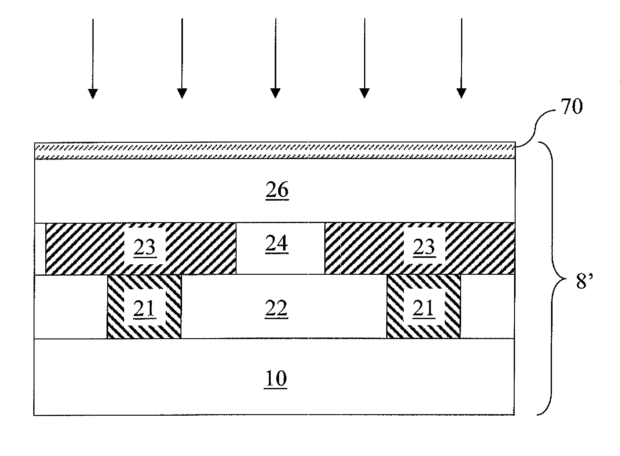
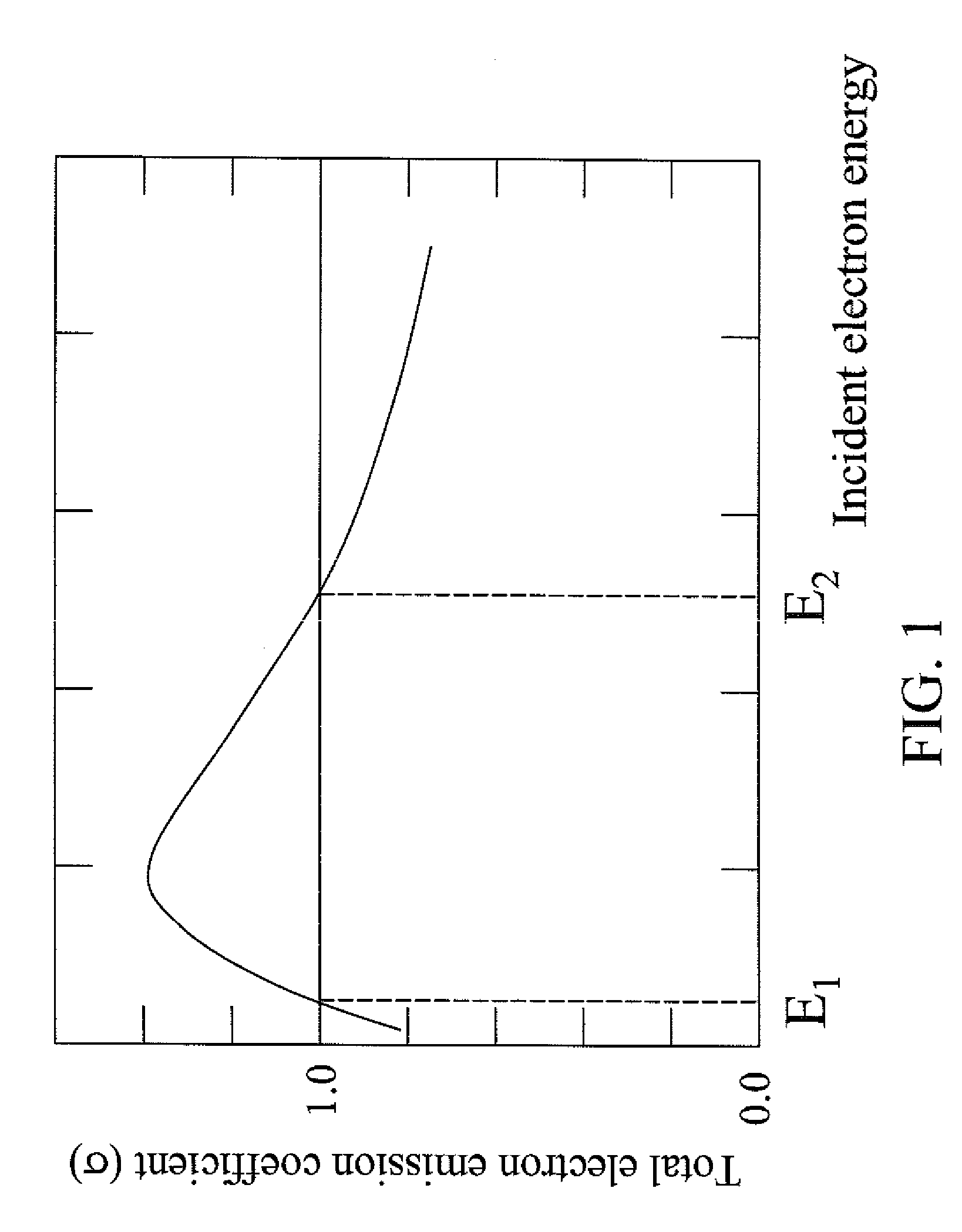
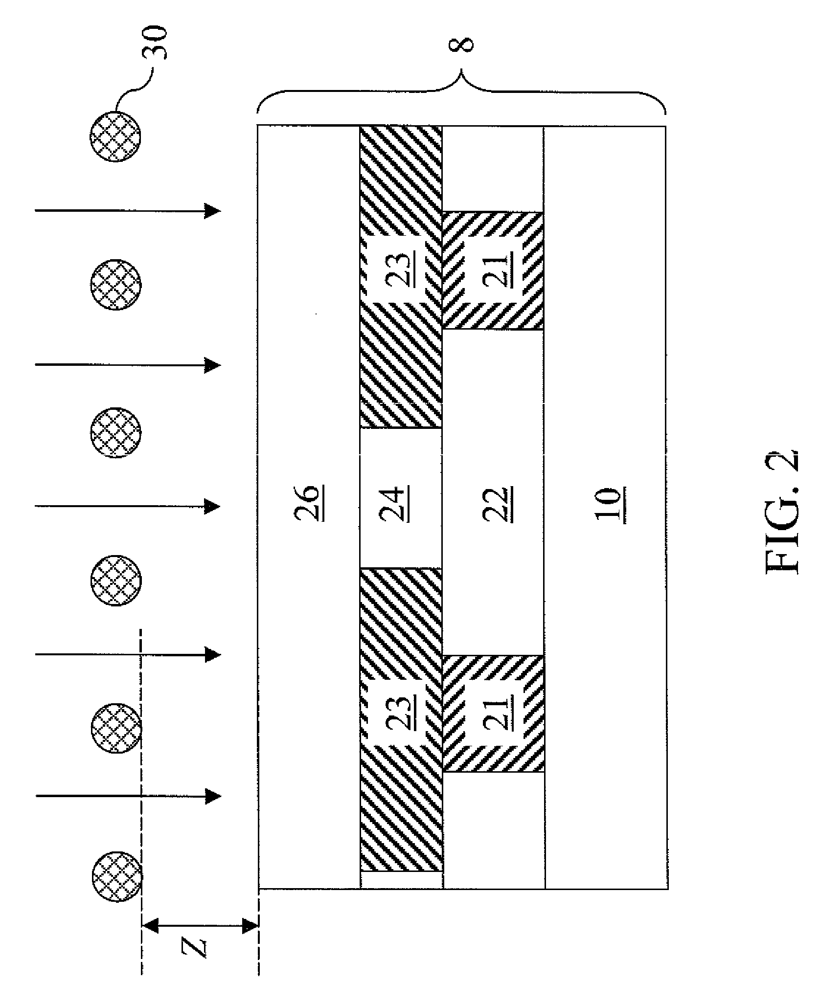
- A method involving the use of a grid of wires or a polymeric conductive layer electrically biased to maintain a total electron emission coefficient of 1.0 during electron beam curing, ensuring the semiconductor substrate remains neutral and preventing charging, thus enhancing the integration of ultra low-k dielectric materials without damaging adjacent devices.

Methods and apparatus for curing dielectric material
PatentActiveUS20220351969A1
Innovation
- The method involves using an electron beam reactive plasma curing process to stabilize dielectric materials formed by FCVD, specifically by delivering a process gas to a process volume, applying RF power to a high secondary electron emission coefficient electrode to generate a plasma and an electron beam, and contacting the dielectric material with the electron beam to cure it, thereby reducing oxygen content and increasing nitrogen content, thus improving material stability and reducing defects.


Safety Standards and Regulations for E-beam Material Processing
The regulatory landscape for electron beam material processing encompasses multiple international and national standards that govern equipment design, operational procedures, and worker safety protocols. The International Electrotechnical Commission (IEC) provides foundational standards through IEC 60601 series for medical applications and IEC 62274 for industrial electron beam equipment. These standards establish baseline requirements for radiation shielding, beam containment, and emergency shutdown systems that directly impact dielectric material selection and processing parameters.
Radiation safety regulations form the cornerstone of e-beam processing compliance, with organizations such as the International Atomic Energy Agency (IAEA) and national regulatory bodies like the Nuclear Regulatory Commission (NRC) in the United States establishing dose limits and exposure guidelines. The Code of Federal Regulations Title 21 CFR 1020.32 specifically addresses performance standards for cabinet x-ray systems used in industrial applications, while 10 CFR Part 20 governs radiation protection standards that affect facility design and material handling procedures.
Occupational safety standards under OSHA 29 CFR 1910 mandate comprehensive safety programs including personnel training, hazard communication, and emergency response procedures. These regulations require detailed documentation of material properties, processing parameters, and potential hazard scenarios when working with dielectric materials under electron beam exposure. The European Union's Machinery Directive 2006/42/EC and EMC Directive 2014/30/EU establish additional requirements for equipment certification and electromagnetic compatibility that influence system design and material selection criteria.
Environmental regulations increasingly impact e-beam processing operations, particularly regarding volatile organic compound emissions and waste disposal. The Clean Air Act amendments and corresponding state regulations may restrict certain dielectric materials or require specific emission control systems. Additionally, REACH regulations in Europe mandate comprehensive chemical safety assessments for materials used in industrial processes, affecting the selection and documentation requirements for dielectric substrates and processing aids in electron beam applications.
Environmental Impact Assessment of Dielectric E-beam Processing
The environmental implications of dielectric electron beam processing represent a critical consideration in the adoption and scaling of this technology across industrial applications. Unlike traditional thermal processing methods, electron beam processing operates at ambient temperatures, significantly reducing energy consumption and associated carbon emissions. This fundamental advantage positions e-beam technology as an environmentally favorable alternative for material modification and sterilization processes.
Energy efficiency constitutes the primary environmental benefit of dielectric e-beam processing. The technology eliminates the need for high-temperature furnaces or chemical solvents, reducing overall energy requirements by up to 70% compared to conventional thermal treatments. The direct energy transfer mechanism inherent in electron beam systems minimizes waste heat generation, contributing to lower facility cooling requirements and reduced indirect energy consumption.
Chemical waste reduction represents another significant environmental advantage. Traditional dielectric processing often relies on hazardous solvents, acids, or other chemical agents that require careful disposal and generate toxic byproducts. Electron beam processing eliminates most chemical intermediates, producing minimal secondary waste streams and reducing the environmental burden associated with chemical handling, storage, and disposal protocols.
The atmospheric impact of dielectric e-beam processing varies depending on the specific materials and processing conditions employed. While the technology generally produces fewer volatile organic compounds compared to chemical alternatives, certain dielectric materials may release trace amounts of decomposition products under electron bombardment. However, these emissions typically remain well below regulatory thresholds and can be effectively managed through standard ventilation systems.
Lifecycle assessment considerations reveal that electron beam equipment manufacturing requires significant initial resource investment, particularly for high-energy accelerator components containing rare earth elements. However, the extended operational lifespan of e-beam systems, combined with their reduced consumable requirements, generally results in favorable long-term environmental profiles compared to alternative processing technologies.
Waste stream management in dielectric e-beam processing primarily involves handling of spent dielectric materials and occasional replacement of system components. The absence of chemical waste streams simplifies disposal protocols and reduces environmental monitoring requirements, though proper handling of irradiated materials remains essential to ensure compliance with radiation safety standards.
Unlock deeper insights with PatSnap Eureka Quick Research — get a full tech report to explore trends and direct your research. Try now!
Generate Your Research Report Instantly with AI Agent
Supercharge your innovation with PatSnap Eureka AI Agent Platform!