

Evaluating Impact Of Pattern Overlaps In Multi-layer Electron Beam Lithography
APR 28, 20269 MIN READ
Generate Your Research Report Instantly with AI Agent
PatSnap Eureka helps you evaluate technical feasibility & market potential.
Multi-layer EBL Pattern Overlap Background and Objectives
Electron beam lithography has emerged as a cornerstone technology for advanced semiconductor manufacturing and nanofabrication processes, enabling the creation of features with sub-10 nanometer resolution. As device architectures become increasingly complex, multi-layer EBL processes have become essential for fabricating three-dimensional nanostructures, advanced memory devices, and quantum electronic components. However, the precision required for these applications introduces significant challenges related to pattern alignment and overlay accuracy across multiple lithographic layers.
Pattern overlap in multi-layer EBL refers to the phenomenon where features from different lithographic layers intersect or align with varying degrees of precision. This overlap can occur intentionally as part of the device design or unintentionally due to alignment errors, substrate distortion, or systematic process variations. The impact of these overlaps extends beyond simple geometric considerations, affecting critical device parameters including electrical performance, mechanical stability, and manufacturing yield.
The evolution of EBL technology has progressed from single-layer patterning in the 1970s to sophisticated multi-layer processes capable of creating complex three-dimensional architectures. Early applications focused primarily on mask making and research prototyping, where pattern overlap effects were relatively manageable. However, as EBL transitioned into direct-write manufacturing for specialized applications such as photonic devices, MEMS structures, and advanced logic circuits, the cumulative effects of pattern overlaps across multiple layers became increasingly critical.
Contemporary multi-layer EBL processes typically involve 3-15 lithographic layers, each requiring precise alignment to previously patterned features. The challenge intensifies as feature sizes shrink and overlay tolerances tighten, often requiring alignment accuracy better than 5 nanometers across the entire substrate. Pattern overlap effects manifest in various forms, including dose modulation at feature intersections, proximity effects between overlapping structures, and mechanical stress concentration at layer interfaces.
The primary objective of evaluating pattern overlap impacts is to establish predictive models that enable process optimization and yield enhancement. This involves developing comprehensive understanding of how geometric overlap configurations influence final device characteristics, establishing design rules that minimize adverse overlap effects, and creating correction algorithms that compensate for systematic overlay variations. Additionally, the evaluation aims to identify optimal exposure strategies that balance throughput requirements with pattern fidelity across all lithographic layers.
Market Demand for Advanced Multi-layer EBL Applications
The semiconductor industry's relentless pursuit of smaller feature sizes and higher device densities has created substantial market demand for advanced multi-layer electron beam lithography applications. As traditional photolithography approaches fundamental physical limitations, particularly for nodes below 7nm, the industry increasingly relies on EBL for critical patterning steps in advanced logic and memory devices. This transition has generated significant commercial opportunities across multiple market segments.
Advanced memory applications represent one of the most promising market segments for multi-layer EBL technology. Three-dimensional NAND flash memory structures require precise layer-to-layer alignment and pattern fidelity across dozens of stacked layers. The complexity of these structures demands sophisticated lithographic solutions capable of managing pattern overlaps while maintaining critical dimension uniformity. Similarly, emerging memory technologies such as resistive RAM and phase-change memory rely heavily on multi-layer EBL for prototype development and small-volume production.
The photomask industry constitutes another critical market driver for advanced multi-layer EBL applications. As semiconductor manufacturers push toward extreme ultraviolet lithography for high-volume production, the corresponding photomasks require unprecedented pattern accuracy and defect control. Multi-layer EBL systems enable the fabrication of these complex masks by providing the resolution and overlay precision necessary for next-generation lithographic templates.
Research institutions and universities represent a growing market segment with distinct requirements for multi-layer EBL capabilities. Academic research facilities increasingly demand flexible, high-resolution lithographic tools for exploring novel device architectures and materials. The ability to evaluate and optimize pattern overlap effects becomes crucial for advancing fundamental understanding of nanoscale device physics and developing next-generation semiconductor technologies.
Emerging applications in quantum computing and photonics are creating new market opportunities for specialized multi-layer EBL systems. Quantum device fabrication requires atomic-scale precision in pattern placement and minimal overlay errors between critical layers. Similarly, integrated photonic circuits demand precise alignment between optical and electronic components across multiple lithographic layers, driving demand for advanced EBL solutions with enhanced pattern overlap evaluation capabilities.
The market demand is further amplified by the increasing complexity of heterogeneous integration approaches, where different semiconductor technologies are combined within single packages. These advanced packaging solutions require sophisticated multi-layer patterning capabilities to achieve the necessary interconnect densities and alignment tolerances, creating sustained demand for EBL systems capable of managing complex pattern overlap scenarios across diverse material systems.
Current EBL Pattern Overlap Challenges and Limitations
Multi-layer electron beam lithography faces significant pattern overlap challenges that fundamentally limit its effectiveness in advanced semiconductor manufacturing. The primary issue stems from the inherent difficulty in achieving precise alignment between successive lithographic layers, where even nanometer-scale deviations can result in critical dimension variations and device performance degradation. Current overlay accuracy requirements have reached sub-5nm levels for advanced nodes, yet existing EBL systems struggle to consistently maintain such precision across large substrate areas.
Stitching errors represent another major limitation in current EBL implementations. When patterns span multiple writing fields, the boundaries between adjacent fields often exhibit dimensional inconsistencies and alignment discrepancies. These stitching artifacts become particularly problematic in multi-layer structures where cumulative errors can compound, leading to significant pattern distortions that affect device yield and reliability.
Thermal drift during extended exposure times poses substantial challenges for pattern overlap accuracy. EBL processes typically require hours to complete complex multi-layer patterns, during which thermal fluctuations cause mechanical instabilities in the system. These thermal effects result in progressive drift of the electron beam position, creating systematic overlay errors that are difficult to compensate through conventional correction methods.
Charging effects on substrate surfaces introduce additional complications for pattern overlap control. Non-conductive or poorly conductive materials accumulate charge during electron beam exposure, deflecting subsequent beam trajectories and causing localized pattern placement errors. This phenomenon is particularly severe in multi-layer processing where different material layers exhibit varying charging characteristics, leading to layer-dependent overlay variations.
Current metrology and feedback systems lack the real-time capability necessary for dynamic overlay correction during EBL processing. Existing measurement techniques typically require post-exposure analysis, preventing immediate correction of detected overlay errors. This limitation forces reliance on predictive models and pre-calibrated correction algorithms, which often prove insufficient for complex multi-layer pattern requirements.
Substrate distortion and mechanical instabilities further constrain overlay accuracy in multi-layer EBL applications. Processing-induced stress, thermal cycling, and handling between lithographic steps can introduce substrate deformations that alter the relative positions of previously patterned layers. These mechanical effects create non-uniform overlay errors across the substrate that are challenging to model and correct effectively.
Existing Pattern Overlap Evaluation Methods
01 Alignment and registration techniques for multi-layer patterns
Methods for precise alignment and registration of multiple electron beam lithography layers to minimize pattern overlaps and ensure accurate positioning. These techniques involve the use of alignment marks, registration systems, and feedback control mechanisms to maintain layer-to-layer accuracy during the lithographic process.- Alignment and registration techniques for multi-layer patterns: Methods for precise alignment and registration of multiple electron beam lithography layers to minimize pattern overlaps and ensure accurate positioning. These techniques involve the use of alignment marks, fiducial markers, and automated positioning systems to maintain layer-to-layer registration accuracy during the lithography process.
- Overlay error correction and compensation methods: Techniques for detecting, measuring, and correcting overlay errors between different lithography layers. These methods include real-time monitoring systems, feedback control mechanisms, and mathematical algorithms to compensate for systematic and random overlay errors that occur during multi-layer pattern formation.
- Pattern stitching and field boundary management: Approaches for managing pattern continuity across field boundaries and stitching adjacent exposure fields in multi-layer electron beam lithography. These techniques address the challenges of maintaining pattern integrity when writing large-area patterns that span multiple exposure fields or writing areas.
- Dose modulation and exposure control strategies: Methods for controlling electron beam dose and exposure parameters in overlapping regions of multi-layer patterns. These strategies involve adaptive dose correction, proximity effect compensation, and exposure sequence optimization to prevent over-exposure or under-exposure in pattern overlap areas.
- Multi-pass writing and layer sequencing optimization: Techniques for optimizing the sequence and methodology of writing multiple layers in electron beam lithography to minimize pattern distortion and improve overlay accuracy. These approaches include multi-pass exposure strategies, layer-dependent writing parameters, and optimized processing sequences for complex multi-layer structures.
02 Overlay error correction and compensation methods
Techniques for detecting, measuring, and correcting overlay errors between different lithographic layers. These methods include real-time monitoring systems, error measurement algorithms, and compensation strategies to reduce pattern misalignment and improve overall lithographic accuracy.Expand Specific Solutions03 Multi-pass exposure strategies and dose control
Approaches for controlling electron beam exposure in multiple passes to achieve desired pattern characteristics while managing overlap regions. These strategies involve optimized dose distribution, exposure sequencing, and beam control techniques to ensure uniform pattern formation across overlapping areas.Expand Specific Solutions04 Pattern stitching and field boundary management
Methods for seamlessly connecting patterns across different exposure fields and managing boundaries between adjacent lithographic areas. These techniques address field stitching errors, boundary effects, and ensure continuity of patterns across multiple exposure regions.Expand Specific Solutions05 Resist processing and development optimization for overlapped regions
Specialized resist processing techniques and development procedures optimized for areas where multiple lithographic patterns overlap. These methods involve tailored resist formulations, development parameters, and post-exposure treatments to achieve uniform pattern quality in overlap regions.Expand Specific Solutions
Key Players in EBL Equipment and Process Development
The multi-layer electron beam lithography pattern overlap evaluation represents a critical challenge in the mature semiconductor lithography industry, which has reached a market size exceeding $20 billion annually. The industry is currently in an advanced consolidation phase, with established equipment manufacturers like ASML, Canon, and NuFlare Technology leading lithography systems development, while foundries including TSMC, Samsung Electronics, and SK Hynix drive manufacturing innovation. Technology maturity varies significantly across segments - companies like D2S and Aselta Nanographics specialize in advanced e-beam software solutions for pattern optimization, while research institutions such as Fudan University and Naval Research Laboratory contribute fundamental algorithmic developments. The competitive landscape shows high technical barriers with specialized players like Carl Zeiss SMS and JEOL focusing on precision instrumentation, indicating a technology approaching commercial maturity but requiring continued innovation in pattern fidelity and overlay accuracy for next-generation semiconductor nodes.
ASML Netherlands BV
Technical Solution: ASML has developed advanced computational lithography solutions that address pattern overlap challenges in multi-layer electron beam lithography through sophisticated proximity effect correction algorithms and dose optimization techniques. Their approach utilizes machine learning-based pattern recognition to predict and compensate for inter-layer interference effects, enabling precise control of critical dimensions across multiple lithographic layers. The company's EUV lithography systems incorporate real-time pattern overlap detection and correction mechanisms that can adjust exposure parameters dynamically to minimize overlay errors and maintain pattern fidelity in complex multi-layer structures.
Strengths: Industry-leading lithography expertise with comprehensive overlay correction capabilities and advanced computational algorithms. Weaknesses: High system complexity and cost, requiring significant infrastructure investment for implementation.
Hitachi High-Tech America, Inc.
Technical Solution: Hitachi High-Tech has developed electron beam lithography systems with advanced pattern overlap analysis capabilities, focusing on multi-beam writing strategies that minimize inter-layer pattern interference. Their technology employs sophisticated beam control algorithms that can dynamically adjust exposure sequences and dose distributions to account for pattern density variations across different layers. The system incorporates real-time metrology feedback to monitor pattern overlap effects and automatically optimize writing parameters to maintain critical dimension uniformity and minimize proximity effects in multi-layer structures.
Strengths: Advanced multi-beam technology with real-time feedback control and proven track record in high-resolution lithography applications. Weaknesses: Limited market presence compared to major competitors and higher operational complexity requiring specialized expertise.
Core Technologies for Pattern Overlap Impact Analysis
Method and system for design of enhanced accuracy patterns for charged particle beam lithography
PatentInactiveUS20120221980A1
Innovation
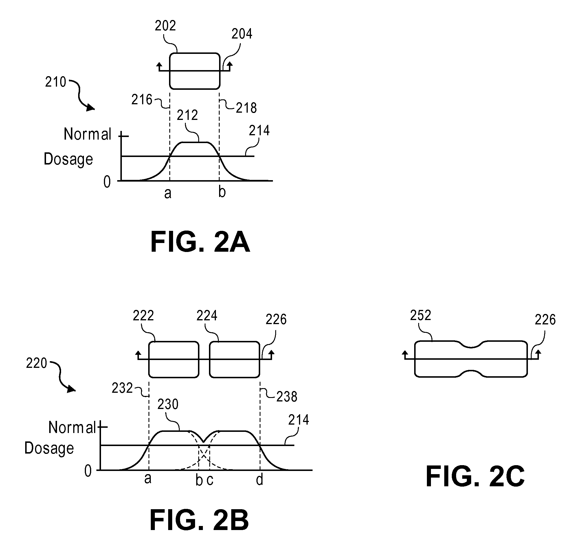
- The method involves generating overlapping shots with varying dosages and sizes to improve the fidelity and critical dimension variation of the transferred pattern, using simulation to determine the optimal pattern on the surface, which can include increasing dosage at edges and corners to enhance edge slope and reduce backscatter effects.

Electron beam lithography method
PatentInactiveUS20040058536A1
Innovation
- The method involves extending the widths of stripes to overlap at boundaries, reducing the electron beam dose in the overlap regions, and performing sequential exposures with reduced doses to minimize butting errors and reduce exposure time.


Metrology Standards for EBL Pattern Characterization
The establishment of robust metrology standards for electron beam lithography pattern characterization has become increasingly critical as multi-layer EBL processes advance toward sub-10nm resolution regimes. Current standardization efforts focus on developing comprehensive measurement protocols that can accurately assess pattern fidelity, overlay precision, and dimensional uniformity across multiple lithographic layers. These standards must address the unique challenges posed by pattern overlap evaluation, where traditional single-layer metrology approaches prove insufficient for capturing the complex interactions between overlapping structures.
International standardization bodies, including SEMI and ISO, are actively developing measurement frameworks specifically tailored for multi-layer EBL applications. These emerging standards emphasize the need for three-dimensional characterization techniques that can distinguish between intended pattern overlaps and undesirable interference effects. The standards incorporate advanced metrology methods such as critical dimension scanning electron microscopy, atomic force microscopy, and scatterometry-based measurements to provide comprehensive pattern analysis capabilities.
Key measurement parameters defined in these standards include overlay accuracy specifications, typically requiring sub-5nm precision for advanced applications, and pattern edge roughness criteria that account for the cumulative effects of multi-layer processing. The standards also establish protocols for measuring pattern contrast degradation and proximity effects that become amplified in overlapping regions. These parameters are essential for quantifying the impact of pattern overlaps on overall lithographic performance.
Calibration procedures represent another crucial aspect of EBL metrology standards, requiring traceable reference materials and standardized test patterns specifically designed for multi-layer overlap assessment. These calibration standards must account for the three-dimensional nature of overlapping patterns and provide reliable benchmarks for equipment qualification and process monitoring. The development of certified reference materials for EBL applications remains an active area of standardization work.
Implementation challenges for these metrology standards include the need for specialized equipment capabilities and trained personnel familiar with multi-layer characterization techniques. The standards must also address data analysis protocols that can effectively process the complex datasets generated by three-dimensional pattern measurements, ensuring consistent interpretation across different facilities and equipment platforms.
Process Control Strategies for Multi-layer EBL Systems
Effective process control strategies for multi-layer electron beam lithography systems are essential to minimize pattern overlap impacts and ensure consistent manufacturing outcomes. These strategies encompass real-time monitoring, adaptive correction mechanisms, and predictive control algorithms that work synergistically to maintain pattern fidelity across multiple lithographic layers.
Real-time metrology integration represents a cornerstone of modern EBL process control. Advanced systems employ in-situ measurement techniques including laser interferometry for stage positioning, electron beam current monitoring, and resist thickness verification. These measurements provide continuous feedback loops that enable immediate corrections during the lithographic process, preventing cumulative errors that could lead to significant pattern overlaps.
Adaptive dose correction algorithms constitute another critical control strategy. These systems dynamically adjust electron beam parameters based on local pattern density, proximity effects, and substrate variations. Machine learning models trained on historical process data can predict optimal dose distributions, accounting for inter-layer interactions and minimizing the risk of pattern distortion that contributes to overlap issues.
Stage positioning control employs sophisticated servo systems with sub-nanometer accuracy. Multi-axis feedback control systems utilize high-resolution encoders and environmental compensation algorithms to maintain precise positioning throughout the exposure process. Advanced systems incorporate predictive motion control that anticipates mechanical disturbances and thermal drift effects.
Environmental control strategies focus on maintaining stable operating conditions that directly impact pattern placement accuracy. Temperature regulation within millikelvin ranges, vibration isolation systems, and electromagnetic field shielding are implemented to minimize external influences on the lithographic process. These environmental controls are particularly crucial for multi-layer applications where small deviations can accumulate across layers.
Automated calibration procedures ensure consistent system performance over extended periods. These include regular beam calibration routines, stage accuracy verification, and resist sensitivity monitoring. Predictive maintenance algorithms analyze system performance trends to schedule calibrations before drift exceeds acceptable tolerances, maintaining the precision required for complex multi-layer pattern registration.
Unlock deeper insights with PatSnap Eureka Quick Research — get a full tech report to explore trends and direct your research. Try now!
Generate Your Research Report Instantly with AI Agent
Supercharge your innovation with PatSnap Eureka AI Agent Platform!