

Comparing Efficiency of Single vs Multi-Junction Semiconductor Devices
MAR 31, 20269 MIN READ
Generate Your Research Report Instantly with AI Agent
PatSnap Eureka helps you evaluate technical feasibility & market potential.
Semiconductor Junction Technology Background and Objectives
Semiconductor junction technology represents one of the most fundamental and transformative innovations in modern electronics, serving as the cornerstone for virtually all electronic devices from simple diodes to complex integrated circuits. The evolution of this technology has been driven by the continuous pursuit of enhanced efficiency, performance, and functionality in electronic systems.
The historical development of semiconductor junctions began with the discovery of the rectifying properties of crystal detectors in the early 20th century, progressing through the invention of the transistor in 1947 to today's sophisticated multi-junction architectures. This technological journey has been characterized by relentless miniaturization, improved material science, and increasingly complex device structures designed to optimize specific performance parameters.
Single-junction semiconductor devices, characterized by a single p-n interface, have traditionally formed the backbone of electronic systems due to their simplicity, cost-effectiveness, and well-understood operational characteristics. These devices operate on fundamental principles of charge carrier diffusion and drift, creating depletion regions that enable controlled current flow and voltage regulation.
Multi-junction semiconductor devices represent a significant advancement in junction technology, incorporating multiple p-n interfaces within a single device structure. This architectural complexity enables enhanced functionality, improved efficiency, and superior performance characteristics compared to their single-junction counterparts. The integration of multiple junctions allows for sophisticated control mechanisms and optimized energy conversion processes.
The primary objective of advancing semiconductor junction technology centers on maximizing device efficiency while maintaining operational reliability and cost-effectiveness. Efficiency optimization encompasses multiple dimensions including power conversion efficiency, spectral response optimization, thermal management, and overall system performance enhancement.
Contemporary research and development efforts focus on achieving breakthrough improvements in junction design, material selection, and manufacturing processes. The integration of novel semiconductor materials, advanced doping techniques, and precision fabrication methods aims to push the theoretical and practical limits of junction device performance.
The comparative analysis of single versus multi-junction architectures has become increasingly critical as applications demand higher efficiency standards and more sophisticated functionality. This technological assessment drives strategic decisions in product development, manufacturing investments, and long-term research directions across the semiconductor industry.
Market Demand for High-Efficiency Semiconductor Devices
The global semiconductor market is experiencing unprecedented demand for high-efficiency devices, driven by the convergence of multiple technological megatrends. Energy efficiency has become a critical performance metric across virtually all electronic applications, from consumer electronics to industrial systems, creating substantial market opportunities for advanced semiconductor solutions.
The renewable energy sector represents one of the most significant growth drivers for high-efficiency semiconductor devices. Solar photovoltaic systems increasingly require sophisticated power conversion technologies, where multi-junction devices demonstrate superior performance in concentrated photovoltaic applications. Wind energy systems similarly demand efficient power electronics for grid integration and energy conversion, pushing the boundaries of semiconductor efficiency requirements.
Electric vehicle adoption is fundamentally reshaping semiconductor demand patterns. Power electronics for electric drivetrains, charging infrastructure, and battery management systems require devices capable of handling high voltages and currents while maintaining exceptional efficiency. The automotive industry's transition toward electrification has created a substantial addressable market for both single and multi-junction semiconductor technologies, with efficiency directly impacting vehicle range and performance.
Data center infrastructure represents another critical demand driver, where energy efficiency translates directly to operational cost savings and environmental sustainability. Cloud computing growth and artificial intelligence workloads are intensifying power density requirements, making high-efficiency semiconductor devices essential for thermal management and energy consumption optimization.
Telecommunications infrastructure modernization, particularly the deployment of advanced wireless networks, requires power amplifiers and RF components with superior efficiency characteristics. The proliferation of connected devices and increasing data transmission requirements are driving demand for semiconductor solutions that can deliver high performance while minimizing power consumption.
Industrial automation and Internet of Things applications are creating new market segments for efficient semiconductor devices. These applications often operate in power-constrained environments where battery life and thermal management are critical considerations, making efficiency a primary selection criterion for semiconductor components.
The market dynamics favor solutions that can demonstrate measurable efficiency improvements over existing technologies. Cost-performance optimization remains crucial, as customers evaluate the total cost of ownership including energy consumption, thermal management requirements, and system reliability. This creates opportunities for both single-junction devices with optimized designs and multi-junction devices that can justify their higher complexity through superior performance metrics.
Current Status and Challenges in Junction Design
Single-junction semiconductor devices currently dominate the commercial photovoltaic market, with silicon-based solar cells achieving efficiencies of 20-26% in commercial applications. These devices operate on the principle of converting photons within a specific energy range, with excess energy lost as heat through thermalization. The theoretical Shockley-Queisser limit constrains single-junction devices to approximately 33.7% efficiency under standard test conditions, creating a fundamental ceiling for performance improvements.
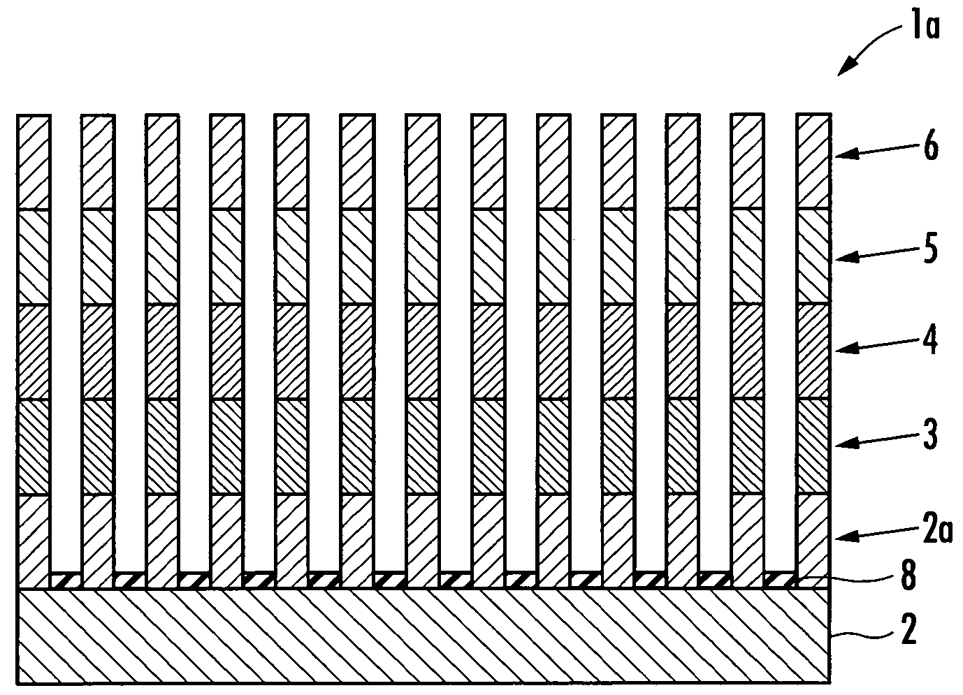
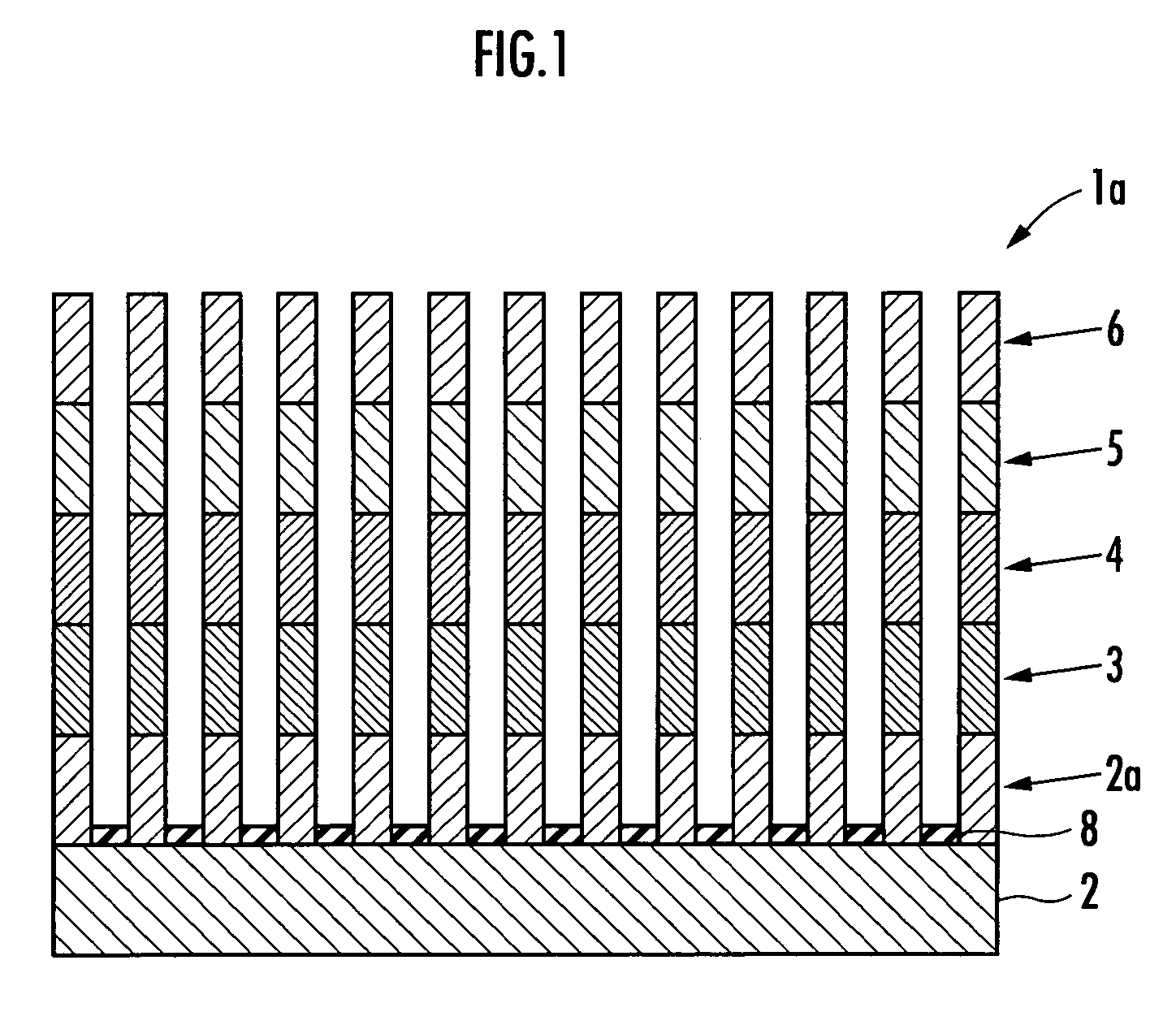
Multi-junction devices represent a significant advancement in semiconductor efficiency, with current triple-junction cells achieving over 40% efficiency in laboratory conditions and commercial concentrator systems reaching 35-38%. These devices stack multiple semiconductor layers with different bandgaps, enabling capture of broader solar spectrum ranges. However, manufacturing complexity increases exponentially with each additional junction, requiring precise lattice matching and sophisticated epitaxial growth techniques.
Current lattice-matching constraints pose substantial challenges in multi-junction design. Traditional approaches rely on materials systems like GaInP/GaAs/Ge, which provide good lattice compatibility but limit bandgap optimization. Metamorphic growth techniques have emerged to address these limitations, allowing greater flexibility in material selection but introducing threading dislocations that can degrade device performance and long-term reliability.
Tunnel junction design represents another critical challenge in multi-junction architectures. These interconnecting layers must provide low-resistance pathways between subcells while maintaining optical transparency. Current designs struggle with series resistance issues, particularly under concentrated illumination, limiting the practical efficiency gains achievable in real-world applications.
Manufacturing scalability remains a significant barrier for multi-junction adoption. While single-junction silicon processing benefits from decades of industrial optimization and economies of scale, multi-junction fabrication requires specialized III-V semiconductor processing with substantially higher material costs. Current production volumes are limited primarily to space applications and concentrated photovoltaic systems where premium efficiency justifies increased costs.
Thermal management challenges intensify with multi-junction complexity. Higher efficiency devices generate more waste heat per unit area, requiring sophisticated cooling systems that add system complexity and cost. Temperature coefficients vary between different junction materials, creating additional design constraints for maintaining optimal performance across operating temperature ranges.
Recent developments in inverted metamorphic multi-junction cells and dilute nitride materials show promise for addressing some current limitations. However, these approaches introduce new challenges related to material quality, processing complexity, and long-term stability that require continued research and development efforts.
Current Junction Efficiency Enhancement Solutions
01 Advanced semiconductor material composition and doping techniques
Improving semiconductor device efficiency through optimized material selection and doping processes. This includes the use of specific semiconductor compounds, controlled impurity introduction, and material layer engineering to enhance electrical properties and reduce energy losses. Advanced doping profiles and material compositions enable better charge carrier mobility and reduced resistance in semiconductor devices.- Advanced semiconductor material composition and doping techniques: Improving semiconductor device efficiency through optimized material selection and doping processes. This includes the use of specific semiconductor compounds, controlled impurity introduction, and material layer engineering to enhance electrical properties and reduce energy losses. Advanced doping profiles and material compositions enable better charge carrier mobility and reduced resistance in semiconductor devices.
- Device structure optimization and geometric design: Enhancement of semiconductor device efficiency through innovative structural configurations and geometric arrangements. This involves optimizing device architecture, layer thickness, junction designs, and three-dimensional structures to improve current flow, reduce parasitic effects, and maximize active area utilization. Structural modifications can significantly impact device performance and power conversion efficiency.
- Thermal management and heat dissipation solutions: Improving semiconductor device efficiency through enhanced thermal management techniques. This includes the integration of heat sinks, thermal interface materials, and cooling structures to effectively dissipate heat generated during device operation. Proper thermal management prevents performance degradation, extends device lifetime, and maintains optimal operating temperatures for improved efficiency.
- Interface engineering and contact optimization: Enhancement of semiconductor device efficiency through improved interface quality and contact resistance reduction. This involves optimizing metal-semiconductor contacts, reducing interface defects, and implementing barrier layers to minimize energy losses at junctions. Advanced interface engineering techniques enable better charge injection and extraction, leading to improved overall device performance.
- Power conversion and energy harvesting optimization: Improving semiconductor device efficiency through advanced power conversion circuits and energy harvesting mechanisms. This includes optimized switching techniques, reduced switching losses, and enhanced energy capture from various sources. Integration of intelligent control systems and adaptive algorithms enables maximum power point tracking and efficient energy utilization in semiconductor devices.
02 Device structure optimization and geometric design
Enhancement of semiconductor device efficiency through innovative structural designs and geometric configurations. This involves optimizing device architecture, layer thickness, junction designs, and three-dimensional structures to improve current flow and minimize power dissipation. Structural modifications can significantly impact device performance by reducing parasitic effects and improving heat dissipation.Expand Specific Solutions03 Thermal management and heat dissipation solutions
Improving semiconductor device efficiency through enhanced thermal management techniques. This includes the integration of heat sinks, thermal interface materials, and cooling structures to maintain optimal operating temperatures. Effective thermal management prevents performance degradation and extends device lifetime by reducing temperature-related efficiency losses.Expand Specific Solutions04 Interface engineering and contact optimization
Enhancement of semiconductor device efficiency by optimizing interfaces between different materials and improving electrical contacts. This involves surface treatment methods, barrier layer formation, and contact metallization techniques to reduce contact resistance and interface defects. Proper interface engineering minimizes energy losses at material boundaries and improves overall device conductivity.Expand Specific Solutions05 Power conversion and switching efficiency improvements
Techniques for enhancing the efficiency of semiconductor devices in power conversion and switching applications. This includes circuit topology optimization, gate drive improvements, and switching loss reduction methods. Advanced control strategies and device configurations enable faster switching speeds with lower energy losses, improving overall system efficiency in power electronic applications.Expand Specific Solutions
Major Players in Advanced Semiconductor Manufacturing
The semiconductor device efficiency comparison market represents a mature yet rapidly evolving sector driven by increasing demand for power-efficient electronics across automotive, mobile, and industrial applications. The industry is experiencing significant growth, with market size expanding due to electric vehicle adoption and 5G infrastructure deployment. Technology maturity varies considerably between single-junction and multi-junction approaches, with established players like Samsung Electronics, Intel, and Toshiba leading single-junction innovations through advanced process nodes and materials engineering. Multi-junction technology shows emerging maturity, particularly in specialized applications, with companies like Alta Devices pioneering gallium arsenide solutions and Soitec advancing silicon-on-insulator substrates. The competitive landscape features traditional semiconductor giants alongside specialized firms like IceMos Technology and Alpha & Omega Semiconductor, while foundries such as GlobalFoundries enable broader market access. Key technological differentiators include power efficiency optimization, thermal management, and integration capabilities, positioning this sector for continued innovation-driven growth.
Samsung Electronics Co., Ltd.
Technical Solution: Samsung develops both single-junction silicon and multi-junction compound semiconductor devices for various applications including power management and RF systems. Their approach combines traditional CMOS processes with advanced III-V materials for heterojunction bipolar transistors and high-electron-mobility transistors. The company leverages its foundry capabilities to optimize device architectures, comparing single-junction silicon FETs with multi-junction HEMTs for 5G infrastructure and automotive power electronics, focusing on efficiency improvements through bandgap engineering and reduced parasitic losses.
Strengths: Large-scale manufacturing capabilities, diverse application portfolio, integrated design-to-production workflow. Weaknesses: Less specialized than pure-play compound semiconductor companies, higher complexity in multi-junction processes.
Infineon Technologies Austria AG
Technical Solution: Infineon focuses on power semiconductor efficiency comparison between single-junction silicon devices and multi-junction wide-bandgap semiconductors like silicon carbide and gallium nitride. Their research demonstrates that multi-junction SiC devices achieve 15-20% higher efficiency in power conversion applications compared to single-junction silicon IGBTs. The company develops hybrid approaches combining silicon with compound semiconductors to optimize switching losses, thermal management, and overall system efficiency for automotive and industrial power electronics applications.
Strengths: Strong power electronics expertise, proven wide-bandgap technology, automotive market leadership. Weaknesses: Limited presence in high-frequency applications, higher material costs for compound semiconductors.
Core Patents in Multi-Junction Device Architecture
Method implemented in a computer for the numerical simulation of semiconductor devices comprising tunnel junctions
PatentInactiveEP2372586A1
Innovation
- A distributed model for semiconductor devices that incorporates a combination of a functional element and resistors to simulate the tunnel junction's behavior, allowing for the representation of the tunnel junction's characteristic curve with four regions (ohmic, negative resistance, excess current, and diode regions), which improves numerical stability and avoids convergence problems.


Method for producing multijunction solar cell
PatentInactiveUS7615400B2
Innovation
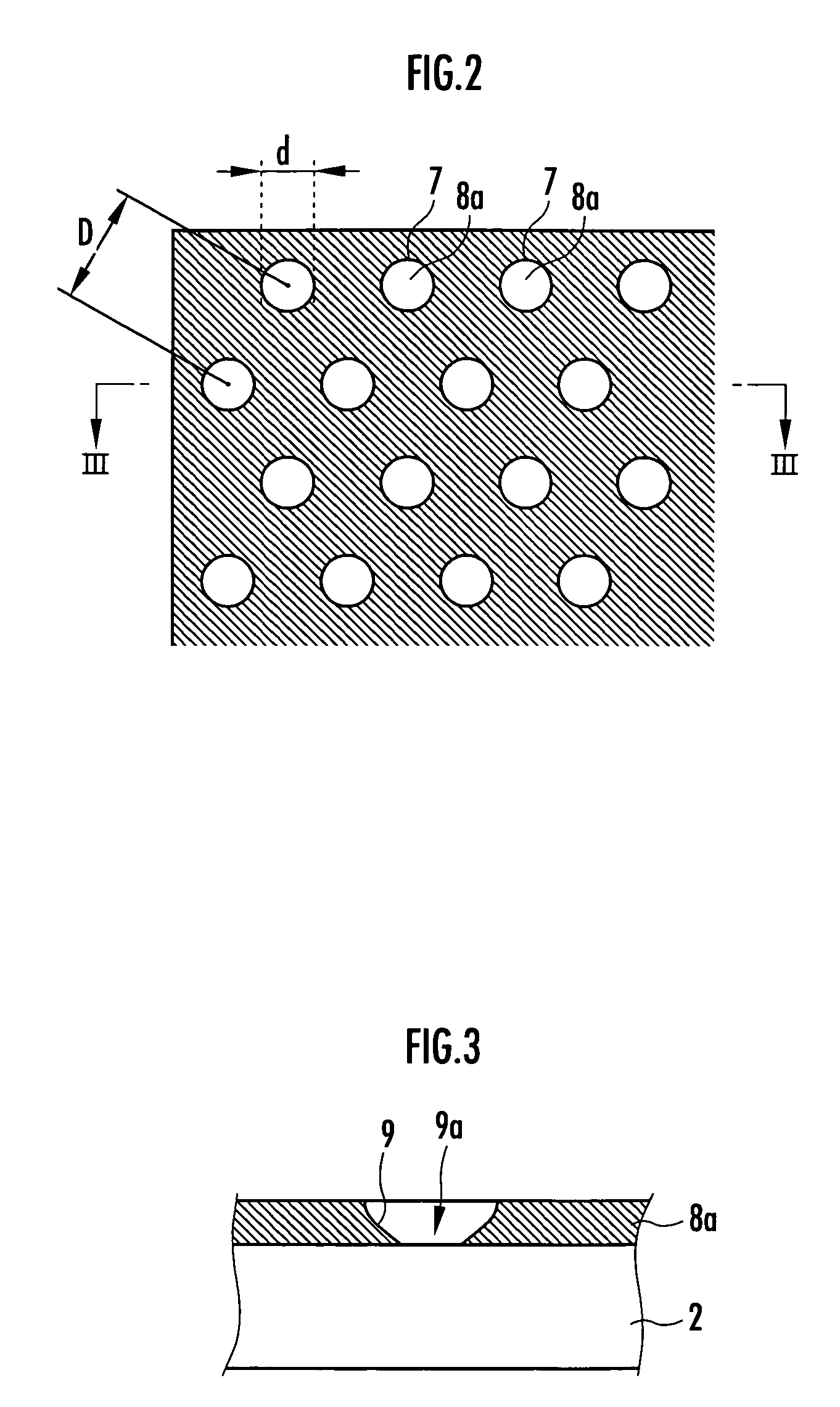
- A method involving the growth of wire-shaped semiconductors with successive epitaxial growth of single-junction solar cells, where each semiconductor has a narrower band gap than the previous one, allowing for the formation of a four-junction solar cell with reduced junction interface area and minimized defects by using materials like GaP, Al0.3Ga0.7As, GaAs, In0.3Ga0.7As, and In0.6Ga0.4As.

Energy Policy Impact on Semiconductor Efficiency Standards
Energy policy frameworks worldwide are increasingly establishing stringent efficiency standards for semiconductor devices, directly influencing the comparative evaluation between single-junction and multi-junction technologies. The European Union's Green Deal and the United States' CHIPS and Science Act have introduced mandatory efficiency thresholds that favor advanced semiconductor architectures capable of achieving higher energy conversion rates.
Current regulatory trends demonstrate a clear preference for multi-junction devices in applications where efficiency gains justify higher manufacturing costs. The International Energy Agency's semiconductor efficiency roadmap targets a 40% improvement in power conversion efficiency by 2030, creating regulatory pressure that inherently advantages multi-junction technologies over traditional single-junction alternatives.
Government incentive structures are reshaping market dynamics through targeted subsidies and tax credits for high-efficiency semiconductor manufacturing. Countries like Germany and Japan offer substantial financial incentives for companies developing multi-junction solar cells and power electronics, while simultaneously implementing carbon pricing mechanisms that penalize less efficient single-junction devices in certain applications.
Emerging policy frameworks are establishing tiered efficiency classifications that directly impact market access and competitiveness. The proposed Global Semiconductor Efficiency Standards initiative would create mandatory labeling requirements, enabling consumers and industrial buyers to make informed decisions based on standardized efficiency metrics that clearly differentiate single-junction and multi-junction performance characteristics.
Regulatory compliance costs are becoming a significant factor in technology selection decisions. Multi-junction devices, despite higher initial development investments, often provide clearer pathways to meeting future efficiency mandates, while single-junction technologies face increasing regulatory barriers in energy-sensitive applications such as electric vehicle charging infrastructure and renewable energy systems.
Policy-driven research funding allocation is accelerating multi-junction technology development through targeted grants and public-private partnerships. National science foundations are prioritizing research proposals that demonstrate potential for exceeding current efficiency standards, creating an innovation ecosystem that systematically favors advanced junction architectures over conventional single-junction approaches.
Cost-Performance Trade-offs in Junction Design
The cost-performance relationship in semiconductor junction design presents a fundamental trade-off that significantly influences device selection across various applications. Single-junction devices typically offer lower manufacturing costs due to their simplified fabrication processes, requiring fewer epitaxial layers and reduced material complexity. The production yield for single-junction devices remains consistently high, as fewer processing steps minimize the probability of defects that could compromise device functionality.
Multi-junction devices, while delivering superior efficiency performance, incur substantially higher production costs. The epitaxial growth of multiple semiconductor layers with precise thickness control and lattice matching requirements demands advanced manufacturing equipment and extended processing times. Material costs escalate proportionally with the number of junctions, particularly when incorporating expensive III-V compound semiconductors such as gallium arsenide or indium gallium phosphide.
The economic viability of multi-junction devices becomes apparent in applications where efficiency gains justify the premium pricing. Space applications exemplify this scenario, where the cost per watt delivered over the mission lifetime favors high-efficiency multi-junction solar cells despite their elevated initial investment. The reduced system weight and enhanced power density offset the higher device costs through decreased launch expenses and improved mission capabilities.
Conversely, terrestrial applications often favor single-junction devices where cost sensitivity outweighs efficiency considerations. Large-scale photovoltaic installations prioritize cost per watt installed, making silicon-based single-junction cells the dominant choice despite their lower conversion efficiency compared to multi-junction alternatives.
Manufacturing scalability further influences the cost-performance equation. Single-junction device production benefits from mature manufacturing infrastructure and economies of scale, resulting in continuous cost reductions. Multi-junction device manufacturing remains constrained by specialized equipment requirements and limited production volumes, maintaining higher unit costs despite technological advances.
The performance degradation characteristics also impact long-term cost considerations. Multi-junction devices may exhibit different aging behaviors compared to single-junction counterparts, affecting the total cost of ownership over the device operational lifetime. Temperature coefficients and radiation tolerance vary between junction configurations, influencing performance sustainability in specific operating environments.
Emerging manufacturing techniques, including wafer bonding and metamorphic growth, aim to reduce multi-junction device costs while maintaining performance advantages. These technological developments gradually shift the cost-performance balance, potentially expanding multi-junction device adoption into previously cost-prohibitive market segments.
Unlock deeper insights with PatSnap Eureka Quick Research — get a full tech report to explore trends and direct your research. Try now!
Generate Your Research Report Instantly with AI Agent
Supercharge your innovation with PatSnap Eureka AI Agent Platform!