

Optimized Strain in Semiconductor Integrated Devices for Energy Efficiency
MAR 31, 20269 MIN READ
Generate Your Research Report Instantly with AI Agent
PatSnap Eureka helps you evaluate technical feasibility & market potential.
Strain Engineering Background and Energy Efficiency Goals
Strain engineering has emerged as a fundamental technique in semiconductor device optimization, tracing its origins to the early observations of piezoresistive effects in silicon during the 1950s. The field gained significant momentum in the 1990s when researchers discovered that mechanical stress could dramatically alter carrier mobility in silicon-based devices. This breakthrough laid the foundation for modern strain engineering approaches that systematically manipulate crystal lattice structures to enhance electrical properties.
The evolution of strain engineering accelerated with the semiconductor industry's relentless pursuit of Moore's Law scaling. As traditional scaling approaches reached physical limitations around the 65nm technology node, strain engineering became a critical enabler for continued performance improvements. The technique involves introducing controlled mechanical stress into semiconductor materials, either through external mechanical forces or by incorporating materials with different lattice constants within the device structure.
Contemporary strain engineering encompasses multiple methodologies, including process-induced strain, substrate-induced strain, and contact etch stop liner techniques. These approaches have demonstrated remarkable success in enhancing carrier mobility, with improvements exceeding 70% for electron mobility and 35% for hole mobility in advanced CMOS technologies. The technique has become indispensable for maintaining performance scaling in sub-22nm technology nodes.
Energy efficiency goals in modern semiconductor devices are increasingly stringent, driven by the proliferation of mobile computing, Internet of Things applications, and data center power consumption concerns. The primary objective is achieving higher performance per watt ratios while maintaining or reducing overall power consumption. Strain engineering directly addresses these goals by enabling devices to operate at lower voltages while maintaining equivalent switching speeds, thereby reducing dynamic power consumption.
The relationship between strain optimization and energy efficiency manifests through multiple mechanisms. Enhanced carrier mobility reduces channel resistance, allowing for faster switching at reduced supply voltages. Additionally, strain-induced bandgap modifications can optimize threshold voltage characteristics, minimizing leakage currents that contribute to static power consumption. These effects collectively enable significant reductions in both active and standby power consumption.
Current energy efficiency targets for advanced semiconductor devices include achieving sub-threshold slopes approaching the theoretical limit of 60mV/decade at room temperature, reducing supply voltages below 0.7V for high-performance applications, and minimizing standby power to femtojoule levels per operation. Strain engineering serves as a key enabler for reaching these ambitious targets while maintaining the performance levels demanded by modern computing applications.
Market Demand for Energy-Efficient Semiconductor Devices
The global semiconductor industry is experiencing unprecedented demand for energy-efficient devices driven by multiple converging factors. Climate change concerns and stringent environmental regulations are pushing manufacturers across all sectors to reduce power consumption in their electronic systems. This regulatory pressure, combined with rising energy costs, has created a compelling economic incentive for developing more efficient semiconductor solutions.
Mobile computing and Internet of Things applications represent the fastest-growing segments demanding energy-efficient semiconductors. Battery-powered devices require extended operational lifespans while maintaining high performance, creating a direct market need for strain-optimized semiconductor technologies. The proliferation of edge computing devices, wearable electronics, and autonomous sensors has amplified this demand exponentially.
Data centers and cloud computing infrastructure constitute another major market driver. These facilities consume substantial amounts of electricity, making energy efficiency a critical operational concern. Strain engineering in semiconductor devices offers significant potential for reducing power consumption in server processors, memory systems, and networking equipment, directly translating to operational cost savings and improved sustainability metrics.
The automotive industry's transition toward electric vehicles and advanced driver assistance systems has created substantial demand for power-efficient semiconductor solutions. Electric vehicle manufacturers require semiconductors that maximize battery range while supporting complex computational tasks. Strain-optimized devices can enhance power management systems, motor controllers, and onboard computing platforms.
Telecommunications infrastructure modernization, particularly the deployment of 5G networks, demands highly efficient semiconductor components. Base stations and network equipment must operate continuously while minimizing energy consumption to ensure economic viability. Strain engineering techniques can improve the efficiency of radio frequency amplifiers, signal processors, and power management circuits.
Consumer electronics manufacturers face increasing pressure to develop products with longer battery life and reduced environmental impact. Smartphones, tablets, laptops, and smart home devices all benefit from strain-optimized semiconductors that deliver superior performance per watt. Market research indicates that energy efficiency has become a primary purchasing consideration for consumers across multiple device categories.
The renewable energy sector also drives demand for efficient semiconductor devices in solar inverters, wind turbine controllers, and energy storage systems. These applications require robust, efficient power electronics that can operate reliably in challenging environmental conditions while maximizing energy conversion efficiency.
Current Strain Engineering Status and Integration Challenges
Strain engineering in semiconductor devices has evolved from a niche research area to a mainstream technology critical for enhancing device performance and energy efficiency. Current implementations primarily focus on mechanical stress introduction through various techniques including process-induced strain, epitaxial growth on lattice-mismatched substrates, and external mechanical loading. Silicon-on-insulator (SOI) platforms have emerged as preferred substrates for strain implementation due to their superior isolation properties and compatibility with advanced CMOS processes.
The semiconductor industry has successfully deployed several strain engineering approaches in commercial products. Strained silicon channels, achieved through SiGe source/drain regions, have become standard in high-performance transistors, delivering mobility enhancements of 20-40% for electrons and 50-80% for holes. Compressive and tensile strain applications are now routinely integrated into 14nm and smaller technology nodes, with foundries reporting significant improvements in drive current and switching speed.
However, substantial integration challenges persist in scaling strain engineering to advanced nodes and three-dimensional architectures. Thermal budget constraints during device fabrication limit the maximum achievable strain levels, as high-temperature processing steps can relax engineered stress. The interaction between strain fields and dopant diffusion profiles creates complex optimization trade-offs, particularly in ultra-scaled devices where precise control of electrical characteristics is paramount.
Process integration complexity increases exponentially when combining multiple strain techniques within single devices. Cross-contamination between different epitaxial materials, stress-induced defect generation, and maintaining strain uniformity across large wafer areas represent ongoing manufacturing challenges. Advanced packaging technologies, including through-silicon vias and wafer-level packaging, introduce additional mechanical stress that can either enhance or degrade the intended strain effects.
Emerging device architectures such as FinFETs, nanowires, and gate-all-around structures present unique strain engineering opportunities and obstacles. The three-dimensional nature of these devices enables novel strain application methods but complicates stress distribution modeling and control. Interface quality between strained layers becomes increasingly critical as device dimensions shrink, requiring atomic-level precision in material deposition and processing.
Current characterization and metrology capabilities struggle to keep pace with strain engineering requirements. Existing measurement techniques often lack the spatial resolution and sensitivity needed for quantifying strain distributions in nanoscale devices. This measurement gap hinders optimization efforts and creates challenges for process control and yield improvement in high-volume manufacturing environments.
Existing Strain Optimization Solutions for Energy Efficiency
01 Power management and voltage regulation techniques
Advanced power management circuits and voltage regulation methods are employed to optimize energy consumption in semiconductor integrated devices. These techniques include dynamic voltage scaling, adaptive power gating, and intelligent power distribution networks that adjust operating parameters based on workload demands. The implementation of efficient voltage regulators and power converters helps minimize power losses during operation while maintaining performance requirements.- Power management and voltage regulation techniques: Advanced power management circuits and voltage regulation methods are employed to optimize energy consumption in semiconductor integrated devices. These techniques include dynamic voltage scaling, adaptive power gating, and intelligent power distribution networks that adjust operating parameters based on workload demands. The implementation of efficient voltage regulators and power converters helps minimize power losses during operation while maintaining performance requirements.
- Low-power circuit design and architecture optimization: Energy-efficient semiconductor devices utilize specialized circuit designs and architectural improvements to reduce power consumption. This includes the use of low-leakage transistors, optimized logic gates, and energy-aware circuit topologies. Clock gating, power domain partitioning, and sleep mode implementations are integrated to minimize static and dynamic power dissipation during various operational states.
- Thermal management and heat dissipation solutions: Effective thermal management systems are crucial for maintaining energy efficiency in semiconductor integrated devices. These solutions incorporate advanced heat sink designs, thermal interface materials, and temperature monitoring circuits. Active and passive cooling mechanisms work together to maintain optimal operating temperatures, preventing thermal throttling and ensuring consistent energy-efficient performance across varying workload conditions.
- Energy harvesting and power recovery mechanisms: Innovative energy harvesting techniques and power recovery systems are integrated into semiconductor devices to improve overall energy efficiency. These mechanisms capture and reuse energy that would otherwise be wasted, including charge recovery circuits, regenerative power systems, and energy scavenging from ambient sources. Such approaches significantly reduce the net energy consumption of integrated devices.
- Process technology and material innovations: Advanced semiconductor manufacturing processes and novel materials contribute to enhanced energy efficiency in integrated devices. This includes the adoption of smaller process nodes, use of high-k dielectrics, and implementation of advanced substrate materials. These technological improvements reduce parasitic capacitances, lower threshold voltages, and minimize leakage currents, resulting in substantial energy savings without compromising device performance.
02 Low-power circuit design and architecture optimization
Energy-efficient semiconductor devices utilize specialized circuit designs and architectural improvements to reduce power consumption. This includes the implementation of low-leakage transistors, optimized logic gates, and energy-aware circuit topologies. Clock gating, power domain partitioning, and reduced switching activity techniques are incorporated to minimize both dynamic and static power dissipation across the integrated device.Expand Specific Solutions03 Thermal management and heat dissipation solutions
Effective thermal management systems are integrated into semiconductor devices to improve energy efficiency by controlling operating temperatures. These solutions include advanced heat sink designs, thermal interface materials, and on-chip temperature monitoring circuits. Proper thermal management prevents performance degradation and reduces the need for excessive cooling power, thereby improving overall system energy efficiency.Expand Specific Solutions04 Energy harvesting and power recovery mechanisms
Innovative energy harvesting techniques and power recovery circuits are implemented to enhance the energy efficiency of semiconductor integrated devices. These mechanisms capture and reuse energy that would otherwise be wasted, such as through charge recycling circuits and energy scavenging from ambient sources. The recovered energy can be stored or directly utilized to reduce external power requirements.Expand Specific Solutions05 Process technology and material innovations
Advanced semiconductor manufacturing processes and novel materials contribute significantly to energy efficiency improvements. This includes the adoption of smaller process nodes, high-k dielectrics, and low-resistance interconnect materials that reduce parasitic capacitances and resistances. Material innovations such as wide-bandgap semiconductors and advanced substrate technologies enable lower power operation while maintaining or improving device performance.Expand Specific Solutions
Key Players in Strain Engineering and Semiconductor Industry
The optimized strain technology in semiconductor integrated devices represents a mature yet evolving field within the broader semiconductor industry, which has reached a market size exceeding $500 billion globally. The industry is currently in a consolidation phase, with established players like Taiwan Semiconductor Manufacturing Co., Samsung Electronics, Intel Corp., and GlobalFoundries dominating foundry services and advanced process development. Technology maturity varies significantly across market segments, with companies like Advanced Micro Devices and Qualcomm driving innovation in processor architectures, while specialized firms such as Atomera and Zeno Semiconductor focus on novel strain engineering approaches. The competitive landscape shows strong regional clusters, particularly in Asia-Pacific with TSMC, Samsung, and United Microelectronics leading manufacturing capabilities, while European players like Infineon Technologies and X-FAB Semiconductor Foundries maintain specialized market positions in automotive and industrial applications.
Taiwan Semiconductor Manufacturing Co., Ltd.
Technical Solution: TSMC employs advanced strain engineering techniques in their leading-edge process nodes, particularly in 3nm and 5nm technologies. They utilize strained silicon channels through selective epitaxial growth of SiGe source/drain regions to enhance carrier mobility in PMOS devices. Their approach includes optimized stress memorization techniques (SMT) and contact etch stop layer (CESL) stress engineering to achieve up to 15-20% performance improvement while reducing power consumption by 10-15%. The company integrates these strain optimization methods with their FinFET architecture, enabling precise control over channel stress distribution for maximum energy efficiency in high-performance computing and mobile applications.
Strengths: Industry-leading process technology, extensive R&D capabilities, proven track record in strain engineering implementation. Weaknesses: High development costs, complex manufacturing processes requiring sophisticated equipment and expertise.
International Business Machines Corp.
Technical Solution: IBM has pioneered several strain engineering innovations including strained silicon-on-insulator (sSOI) technology and advanced epitaxial growth techniques for enhanced device performance. Their research focuses on novel strain engineering approaches using SiGe virtual substrates and selective area growth methods to optimize carrier transport properties. IBM's strain optimization methodology incorporates advanced stress modeling and characterization techniques, enabling precise control over channel stress for improved energy efficiency. The company has developed innovative approaches to strain transfer optimization and stress relaxation mitigation, contributing to enhanced device reliability and performance. Their work includes exploration of alternative channel materials and strain engineering techniques for next-generation semiconductor devices targeting improved energy efficiency metrics.
Strengths: Strong research and development capabilities, innovative strain engineering approaches, extensive intellectual property portfolio. Weaknesses: Limited manufacturing scale compared to pure-play foundries, focus primarily on research rather than high-volume production.
Core Patents in Strain Engineering for Power Reduction
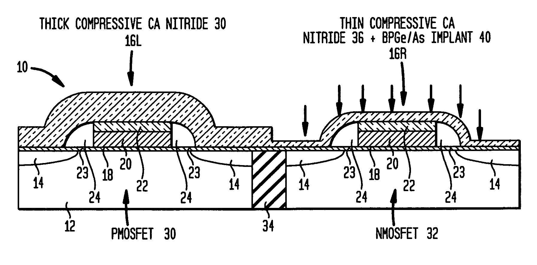
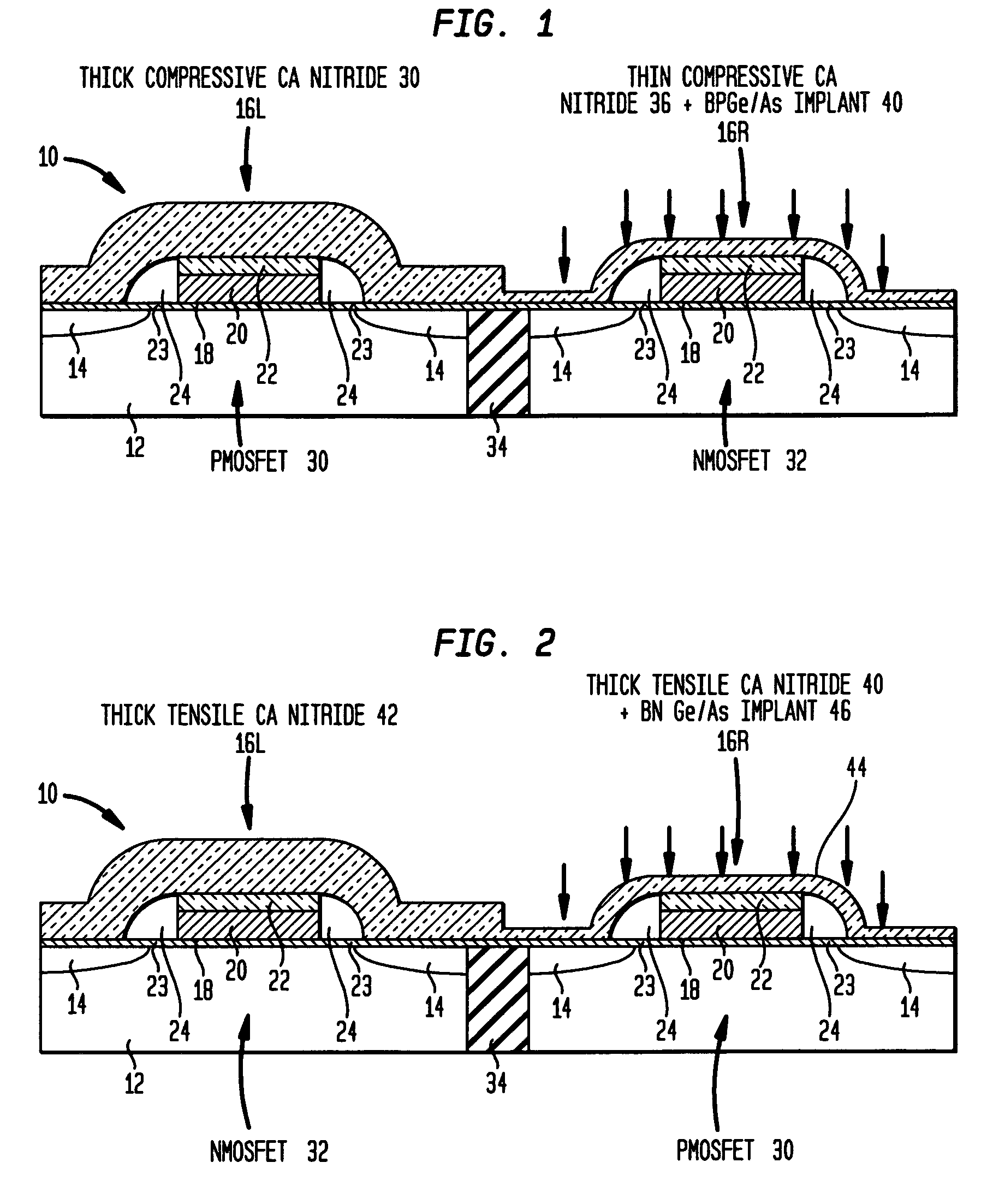
Structure and method to optimize strain in cmosfets
PatentInactiveUS20060157795A1
Innovation
- The method involves forming a strain-inducing CA nitride coating of full thickness on one type of MOSFET to maximize strain and etching it to a reduced thickness on the other type to minimize strain, with optional Ge or As implants to further relax stress and improve performance.
Integrated Circuit Transistor Structure with High Germanium Concentration SiGe Stressor
PatentActiveUS20170263749A1
Innovation
- A two-step process involving a separate low-temperature oxidation step and thermal diffusion step is used to convert a low Ge concentration SiGe film into a high Ge concentration SiGe stressor film, eliminating the need for epitaxial formation and allowing for precise control of the Ge profile, applicable to both planar and FinFET devices.


Environmental Impact Assessment of Strain Engineering
The environmental implications of strain engineering in semiconductor devices present a complex landscape of both opportunities and challenges that require comprehensive assessment across multiple dimensions. As the semiconductor industry increasingly adopts strain engineering techniques to enhance energy efficiency, understanding the environmental footprint becomes crucial for sustainable technological advancement.
Manufacturing processes associated with strain engineering introduce specific environmental considerations that differ from conventional semiconductor fabrication. The implementation of strained silicon layers, silicon-germanium heterostructures, and advanced epitaxial growth techniques requires specialized equipment and materials that can impact resource consumption patterns. These processes often demand higher temperature operations, extended processing times, and the use of germanium-based compounds, which collectively influence the carbon footprint of device manufacturing.
Energy consumption during the fabrication phase represents a significant environmental factor. Strain engineering processes typically require molecular beam epitaxy or chemical vapor deposition systems operating at elevated temperatures for extended periods. The precision control needed for achieving optimal strain levels necessitates sophisticated monitoring equipment and clean room environments, contributing to increased energy demands during production phases.
Material utilization efficiency emerges as another critical environmental consideration. Strain engineering often involves the deposition of thin films with precise compositional gradients, potentially leading to material waste during optimization processes. The sourcing and processing of germanium, indium, and other specialty materials used in strain engineering applications raise concerns about resource sustainability and supply chain environmental impacts.
However, the long-term environmental benefits of strain-engineered devices significantly offset manufacturing impacts through enhanced operational efficiency. Devices incorporating optimized strain configurations demonstrate reduced power consumption during operation, translating to decreased energy requirements throughout their operational lifetime. This efficiency improvement becomes particularly significant in large-scale applications such as data centers and mobile computing platforms.
Life cycle assessment studies indicate that strain-engineered semiconductor devices typically achieve environmental payback within 18-24 months of deployment, after which they provide net environmental benefits through reduced operational energy consumption. The extended operational lifetime of these devices, combined with their superior performance characteristics, contributes to reduced electronic waste generation and longer replacement cycles.
Recycling and end-of-life considerations for strain-engineered devices present both challenges and opportunities. While the complex material compositions may complicate traditional recycling processes, the higher value materials used in these devices create economic incentives for advanced recovery techniques, potentially improving overall semiconductor recycling rates.
Manufacturing Cost Analysis for Strain-Optimized Devices
The manufacturing cost structure for strain-optimized semiconductor devices presents a complex economic landscape that significantly differs from conventional semiconductor production. Initial capital expenditure requirements are substantially elevated due to specialized equipment needs, including precision strain measurement tools, advanced epitaxial growth systems, and modified lithography equipment capable of maintaining strain integrity during processing. These infrastructure investments typically increase facility setup costs by 25-40% compared to standard semiconductor manufacturing lines.
Substrate costs represent a major expense category, particularly for devices utilizing silicon-germanium (SiGe) or gallium arsenide (GaAs) substrates that enable superior strain engineering capabilities. Premium substrate materials can cost 3-5 times more than standard silicon wafers, with additional expenses arising from specialized handling and storage requirements to prevent strain relaxation during inventory management.
Process complexity introduces significant operational cost implications through extended manufacturing cycle times and reduced yield rates during initial production phases. Strain-optimized devices typically require 15-30% more processing steps than conventional semiconductors, including additional annealing cycles, precision deposition processes, and multiple strain characterization checkpoints. These extended processes increase labor costs, equipment utilization time, and energy consumption per unit produced.
Quality control and metrology expenses constitute another substantial cost component, as strain-optimized devices demand sophisticated measurement techniques including X-ray diffraction, Raman spectroscopy, and electron microscopy for strain verification. These characterization processes can add 8-12% to overall manufacturing costs but are essential for ensuring device performance specifications.
However, economies of scale projections indicate promising cost reduction potential as production volumes increase. Industry analysis suggests that manufacturing costs could decrease by 40-60% once annual production volumes exceed 100,000 units per product line, primarily through improved yield rates, process optimization, and amortization of specialized equipment investments across larger production runs.
Unlock deeper insights with PatSnap Eureka Quick Research — get a full tech report to explore trends and direct your research. Try now!
Generate Your Research Report Instantly with AI Agent
Supercharge your innovation with PatSnap Eureka AI Agent Platform!