

CVD in MEMS Fabrication: Process Stability and Repeatability
APR 8, 20269 MIN READ
Generate Your Research Report Instantly with AI Agent
PatSnap Eureka helps you evaluate technical feasibility & market potential.
CVD MEMS Fabrication Background and Process Goals
Chemical Vapor Deposition has emerged as a cornerstone technology in MEMS fabrication since the early development of microelectromechanical systems in the 1980s. The technique's ability to deposit thin films with precise thickness control and excellent conformality made it indispensable for creating the complex three-dimensional structures characteristic of MEMS devices. Initially adapted from semiconductor manufacturing, CVD processes have evolved to address the unique challenges posed by MEMS fabrication, including the need for structural materials, sacrificial layers, and protective coatings.
The evolution of CVD in MEMS has been driven by the increasing complexity and miniaturization demands of microdevices. Early MEMS devices relied primarily on silicon-based materials deposited through thermal CVD processes. However, as applications expanded into harsh environments and specialized functions, the technology evolved to incorporate plasma-enhanced CVD, low-pressure CVD, and atomic layer deposition variants. These advancements enabled the deposition of diverse materials including silicon nitride, silicon carbide, diamond-like carbon, and various metal compounds essential for modern MEMS applications.
Current technological trends indicate a shift toward lower temperature processing to accommodate temperature-sensitive substrates and reduce thermal stress. The integration of in-situ monitoring and real-time process control has become increasingly important as device geometries shrink and performance requirements intensify. Advanced precursor chemistry and novel reactor designs are enabling more precise control over film properties and deposition uniformity across large wafers.
The primary technical objectives for CVD in MEMS fabrication center on achieving exceptional process stability and repeatability while maintaining high-quality film properties. Process stability encompasses the ability to maintain consistent deposition rates, film composition, and morphology throughout extended production runs without significant drift or variation. This stability is crucial for ensuring that critical device dimensions and material properties remain within specified tolerances across multiple fabrication cycles.
Repeatability objectives focus on minimizing batch-to-batch variations and ensuring that identical process conditions yield statistically equivalent results. This includes achieving uniform thickness distribution across wafer surfaces, consistent stress profiles, and reproducible electrical and mechanical properties. The target specifications typically require thickness uniformity better than ±2% across 200mm wafers and run-to-run repeatability within ±1% for critical parameters.
Advanced process control strategies aim to minimize the impact of equipment aging, environmental fluctuations, and consumable variations on final device performance. These objectives drive the development of sophisticated monitoring systems, predictive maintenance protocols, and adaptive process control algorithms that can compensate for systematic variations before they impact product quality.
Market Demand for Stable CVD MEMS Manufacturing
The global MEMS market has experienced unprecedented growth driven by the proliferation of smart devices, automotive electronics, and Internet of Things applications. Consumer electronics remain the largest segment, with smartphones, tablets, and wearables incorporating multiple MEMS sensors including accelerometers, gyroscopes, and pressure sensors. The automotive sector represents another critical growth driver, where MEMS devices enable advanced driver assistance systems, tire pressure monitoring, and electronic stability control.
Industrial automation and healthcare applications are emerging as high-value market segments demanding exceptional reliability and performance consistency. In industrial settings, MEMS sensors monitor equipment health, detect vibrations, and ensure process control accuracy. Healthcare applications require MEMS devices for patient monitoring, drug delivery systems, and diagnostic equipment, where device failure can have critical consequences.
The telecommunications infrastructure expansion, particularly with 5G deployment, has created substantial demand for RF MEMS switches and filters. These components require precise dimensional control and consistent electrical properties, making process stability paramount. Data centers and cloud computing infrastructure also rely heavily on MEMS-based environmental monitoring and cooling system controls.
Market dynamics reveal a clear preference for suppliers capable of delivering consistent, high-yield manufacturing processes. Original equipment manufacturers increasingly prioritize supply chain partners who can guarantee reproducible device characteristics across production batches. This trend has intensified as device miniaturization continues and performance tolerances become tighter.
Quality requirements have become more stringent across all application sectors. Automotive applications demand zero-defect manufacturing with statistical process control capabilities. Consumer electronics manufacturers seek suppliers who can maintain consistent performance while scaling production volumes rapidly to meet seasonal demand fluctuations.
The competitive landscape shows that companies with superior process control capabilities command premium pricing and secure long-term supply agreements. Market leaders have invested heavily in advanced process monitoring, real-time feedback systems, and statistical quality control methodologies. This investment in manufacturing excellence has become a key differentiator in winning high-value contracts and maintaining customer relationships in an increasingly competitive marketplace.
Current CVD Process Stability Challenges in MEMS
Chemical Vapor Deposition (CVD) processes in MEMS fabrication face significant stability challenges that directly impact device performance and manufacturing yield. The inherent complexity of MEMS structures, which often require precise dimensional control at the microscale level, makes CVD process variations particularly problematic. Temperature fluctuations during deposition represent one of the most critical stability issues, as even minor variations can lead to non-uniform film thickness, altered material properties, and compromised device functionality.
Precursor delivery systems present another major challenge in maintaining process stability. Inconsistent precursor flow rates, concentration variations, and delivery timing irregularities can result in non-reproducible deposition conditions. These variations are particularly pronounced in batch processing systems where multiple wafers are processed simultaneously, leading to wafer-to-wafer and within-wafer uniformity issues that significantly impact MEMS device performance.
Chamber contamination and surface preparation inconsistencies contribute substantially to process instability. Residual materials from previous depositions, inadequate cleaning protocols, and varying substrate surface conditions create unpredictable nucleation sites and growth patterns. This is especially problematic for MEMS applications where surface roughness and film adhesion are critical parameters affecting device reliability and mechanical properties.
Plasma-enhanced CVD (PECVD) processes, commonly used in MEMS fabrication, introduce additional stability challenges through plasma parameter variations. Power fluctuations, gas composition changes, and electrode conditioning effects can cause significant variations in deposition rates and film properties. The plasma chemistry's sensitivity to chamber conditions makes it particularly difficult to maintain consistent process parameters across extended production runs.
Equipment aging and component wear represent long-term stability challenges that affect process repeatability. Heating elements, gas delivery components, and chamber surfaces undergo gradual changes that alter deposition characteristics over time. These aging effects are often subtle but cumulative, leading to process drift that becomes apparent only after extended operation periods.
Real-time process monitoring limitations further compound stability challenges. Many CVD systems lack adequate in-situ monitoring capabilities, making it difficult to detect and correct process variations during deposition. This limitation prevents immediate corrective actions and often results in entire batches being processed under suboptimal conditions before issues are identified through post-process characterization.
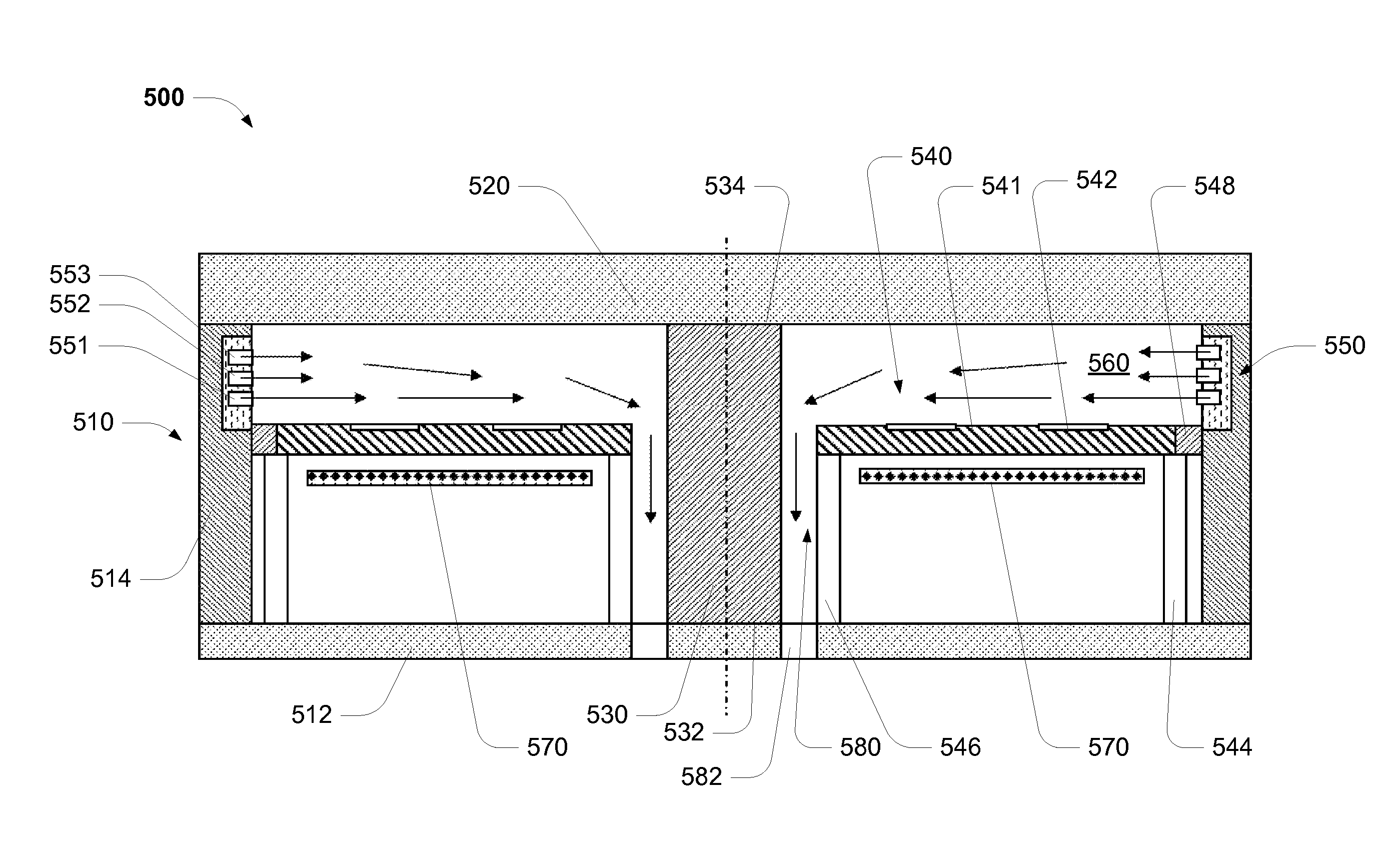
Existing CVD Process Control Solutions for MEMS
01 Process parameter monitoring and control systems
CVD process stability can be enhanced through real-time monitoring and control of critical parameters such as temperature, pressure, gas flow rates, and precursor delivery. Advanced control systems utilize sensors and feedback mechanisms to maintain consistent process conditions throughout deposition cycles. These systems can automatically adjust parameters to compensate for variations and ensure uniform film properties across multiple runs.- Process parameter monitoring and control systems: CVD process stability can be enhanced through real-time monitoring and control of critical process parameters such as temperature, pressure, gas flow rates, and precursor delivery. Advanced control systems utilize sensors and feedback mechanisms to maintain consistent process conditions throughout deposition cycles. These systems can automatically adjust parameters to compensate for variations and ensure uniform film properties across multiple runs.
- Chamber conditioning and cleaning procedures: Maintaining CVD chamber cleanliness and proper conditioning between runs is critical for process repeatability. Regular cleaning protocols remove residual deposits and contaminants that can affect subsequent depositions. Chamber seasoning procedures establish stable surface conditions on reactor walls, reducing particle generation and ensuring consistent gas phase chemistry. Proper maintenance schedules and cleaning techniques minimize process drift over time.
- Precursor delivery and gas distribution optimization: Uniform precursor delivery and gas distribution are essential for achieving repeatable CVD results. Optimized gas injection systems, including showerhead designs and flow distributors, ensure even distribution of reactants across the substrate surface. Precise control of precursor vaporization, mixing ratios, and delivery timing reduces variations in deposition rates and film composition. Advanced delivery systems incorporate mass flow controllers and vapor delivery modules for enhanced stability.
- Temperature uniformity and thermal management: Achieving and maintaining uniform temperature distribution across the substrate and reactor chamber is crucial for CVD process stability. Multi-zone heating systems allow independent control of different reactor regions to compensate for thermal gradients. Proper thermal design includes substrate holder optimization, heating element placement, and insulation strategies. Temperature uniformity directly impacts film thickness distribution, composition, and stress characteristics across wafers.
- In-situ process monitoring and endpoint detection: Real-time in-situ monitoring techniques enable detection of process variations and determination of deposition endpoints for improved repeatability. Optical monitoring methods, including interferometry and spectroscopy, provide non-invasive measurement of film thickness and properties during deposition. Endpoint detection systems ensure consistent film thickness across multiple runs by terminating processes at predetermined conditions. These monitoring capabilities facilitate rapid identification of process excursions and enable corrective actions.
02 Chamber design and gas distribution optimization
Reactor chamber geometry and gas distribution systems play crucial roles in achieving stable and repeatable CVD processes. Optimized showerhead designs, gas injection patterns, and flow dynamics ensure uniform precursor distribution across the substrate surface. Proper chamber design minimizes dead zones, reduces particle generation, and maintains consistent deposition rates across the wafer, leading to improved process repeatability.Expand Specific Solutions03 Precursor delivery and vaporization control
Consistent precursor delivery is essential for CVD process stability. Precise control of precursor vaporization, transport, and injection ensures repeatable film composition and thickness. Systems incorporating mass flow controllers, temperature-controlled delivery lines, and liquid precursor vaporizers help maintain stable precursor concentrations. Proper management of precursor chemistry and delivery mechanisms reduces run-to-run variations.Expand Specific Solutions04 In-situ monitoring and endpoint detection
Real-time process monitoring techniques enable immediate detection of process deviations and ensure repeatability. In-situ measurement methods including optical emission spectroscopy, interferometry, and mass spectrometry provide feedback on film growth rates, composition, and uniformity during deposition. These monitoring capabilities allow for process adjustments and verification of consistent results across multiple runs.Expand Specific Solutions05 Preventive maintenance and chamber conditioning
Regular maintenance protocols and chamber conditioning procedures are critical for maintaining CVD process stability over extended periods. Systematic cleaning schedules, seasoning runs, and component replacement strategies prevent drift in process performance. Proper conditioning of chamber surfaces and establishment of stable thermal and chemical environments ensure consistent baseline conditions for repeatable depositions.Expand Specific Solutions
Key Players in CVD Equipment and MEMS Industry
The CVD in MEMS fabrication market represents a mature yet evolving technological landscape characterized by established semiconductor infrastructure and growing specialization demands. The industry operates in a growth phase driven by IoT expansion and automotive sensor integration, with market size reaching billions annually across semiconductor manufacturing sectors. Technology maturity varies significantly among key players: equipment leaders like Applied Materials, Tokyo Electron, and Veeco Instruments demonstrate advanced CVD capabilities, while foundries including TSMC, Samsung Electronics, and SMIC showcase production-scale implementation. Research institutions such as McGill University and South China University of Technology contribute fundamental innovations, while specialized companies like SilcoTek Corp focus on niche CVD coating applications. The competitive landscape reflects a multi-tiered ecosystem where established semiconductor giants maintain process leadership, emerging players like ASM IP Holding and Semicat provide targeted solutions, and academic partnerships drive next-generation developments, indicating robust technological advancement potential.
Applied Materials, Inc.
Technical Solution: Applied Materials has developed advanced CVD systems specifically for MEMS fabrication with enhanced process control capabilities. Their Centura platform integrates multi-chamber processing with real-time monitoring systems that ensure consistent film deposition across wafer surfaces. The company's CVD technology features precise temperature control within ±1°C variation, advanced gas delivery systems with mass flow controllers achieving ±0.5% accuracy, and in-situ process monitoring using optical emission spectroscopy. Their PECVD systems operate at temperatures as low as 200°C, crucial for MEMS devices with temperature-sensitive components. The platform includes automated recipe management and statistical process control algorithms that maintain repeatability with coefficient of variation below 2% for film thickness uniformity.
Strengths: Industry-leading process control accuracy, comprehensive automation capabilities, excellent temperature uniformity. Weaknesses: High capital investment costs, complex system maintenance requirements.
Tokyo Electron Ltd.
Technical Solution: Tokyo Electron has developed specialized CVD solutions for MEMS applications focusing on low-temperature processing and exceptional repeatability. Their ALPHA series CVD systems incorporate advanced plasma generation technology with dual-frequency RF systems operating at 13.56 MHz and 400 kHz for enhanced process control. The systems feature proprietary gas injection designs that achieve uniformity better than ±2% across 300mm wafers. TEL's CVD platforms include real-time endpoint detection using interferometry and mass spectrometry, enabling precise control of deposition rates and film properties. Their systems maintain chamber-to-chamber matching within ±1.5% for critical parameters, essential for high-volume MEMS production. The company has implemented machine learning algorithms for predictive maintenance and process optimization, reducing unplanned downtime by up to 30%.
Strengths: Excellent chamber-to-chamber matching, advanced plasma control technology, predictive maintenance capabilities. Weaknesses: Limited global service network compared to competitors, higher complexity in system operation.
Core Innovations in CVD Stability and Repeatability
Chemical vapor deposition (CVD) calibration method providing enhanced uniformity
PatentInactiveUS6926920B2
Innovation
- A calibrated source material dispensing nozzle is employed within a CVD apparatus, calibrated and aligned using a calibration and alignment apparatus to ensure optimal flow and uniformity of reactant materials, forming microelectronic layers with improved uniformity.


Chemical vapor deposition reactor and method
PatentInactiveUS8465802B2
Innovation
- A CVD reactor design featuring a cylindrical chamber with a concentrically disposed lid support and an annular gas distribution plate, allowing for horizontal and vertical gas flows that mitigate depletion effects, reduce parasitic reactions, and enhance uniformity, while simplifying construction and reducing costs.

Quality Standards for MEMS CVD Manufacturing
The establishment of comprehensive quality standards for MEMS CVD manufacturing represents a critical foundation for achieving consistent process stability and repeatability across production environments. These standards encompass multiple dimensions of manufacturing control, from raw material specifications to final product validation protocols.
International standards organizations have developed frameworks specifically addressing MEMS fabrication quality requirements. ISO 14644 series standards provide cleanroom classification and monitoring protocols essential for CVD operations, while SEMI standards define equipment qualification procedures and process control methodologies. These frameworks establish baseline requirements for environmental conditions, particle contamination limits, and equipment performance specifications that directly impact CVD process outcomes.
Material quality standards form another crucial component, defining purity levels for precursor gases, substrate specifications, and consumable materials used in CVD processes. These standards typically specify maximum allowable impurity concentrations, moisture content limits, and storage requirements that prevent contamination-induced process variations. Adherence to these material standards significantly reduces sources of process instability and enhances repeatability across production batches.
Process monitoring and control standards establish requirements for real-time parameter tracking, statistical process control implementation, and deviation response protocols. These standards mandate continuous monitoring of critical parameters such as temperature uniformity, pressure stability, gas flow rates, and deposition rates. Statistical control limits are defined based on process capability studies, enabling early detection of process drift before it impacts product quality.
Metrology and inspection standards define measurement protocols for film thickness uniformity, composition analysis, and structural characterization. These standards specify sampling plans, measurement techniques, and acceptance criteria that ensure consistent product quality. Advanced metrology requirements include specifications for measurement uncertainty, calibration procedures, and traceability to national standards.
Documentation and traceability standards establish requirements for process record keeping, batch tracking, and quality system maintenance. These standards ensure complete process history documentation, enabling root cause analysis when quality issues arise and supporting continuous improvement initiatives. Compliance with these comprehensive quality standards provides the foundation for achieving the process stability and repeatability essential for successful MEMS CVD manufacturing operations.
Environmental Impact of CVD MEMS Production
The environmental implications of Chemical Vapor Deposition (CVD) processes in MEMS fabrication present significant challenges that require comprehensive assessment and mitigation strategies. CVD operations typically involve the use of hazardous precursor gases, including silane, dichlorosilane, and various metal-organic compounds, which pose risks to both human health and environmental safety. These materials often exhibit high toxicity, flammability, and potential for atmospheric ozone depletion, necessitating stringent handling protocols and waste management systems.
Energy consumption represents another critical environmental concern in CVD MEMS production. The high-temperature requirements for many CVD processes, often exceeding 600°C, result in substantial energy demands that contribute to carbon footprint expansion. Additionally, the need for ultra-high vacuum systems and continuous gas flow maintenance further amplifies energy consumption throughout the fabrication cycle.
Waste generation from CVD processes encompasses both gaseous emissions and solid byproducts. Unreacted precursors and reaction byproducts released during deposition require sophisticated abatement systems to prevent atmospheric contamination. Solid waste includes contaminated substrates, spent filters, and cleaning materials that often contain hazardous substances requiring specialized disposal methods.
Water usage and contamination present additional environmental challenges, particularly in post-deposition cleaning processes and equipment maintenance. The semiconductor industry's reliance on ultra-pure water systems generates significant wastewater volumes containing chemical residues that demand advanced treatment before discharge.
Recent regulatory developments have intensified focus on sustainable CVD practices, driving adoption of green chemistry principles and alternative precursor materials. Industry initiatives now emphasize process optimization to reduce material consumption, implementation of closed-loop systems for precursor recovery, and development of lower-temperature deposition techniques to minimize energy requirements.
Emerging mitigation strategies include plasma-enhanced CVD at reduced temperatures, atomic layer deposition for precise material usage, and real-time monitoring systems to optimize process efficiency while minimizing environmental impact.
Unlock deeper insights with PatSnap Eureka Quick Research — get a full tech report to explore trends and direct your research. Try now!
Generate Your Research Report Instantly with AI Agent
Supercharge your innovation with PatSnap Eureka AI Agent Platform!