

Diamond Substrates vs Graphene: Conductivity and Cost Efficiency
MAY 14, 20269 MIN READ
Generate Your Research Report Instantly with AI Agent
PatSnap Eureka helps you evaluate technical feasibility & market potential.
Diamond vs Graphene Substrate Development Goals
The development of diamond and graphene substrates represents a critical technological frontier in advanced electronics and quantum applications. Both materials exhibit exceptional properties that position them as next-generation solutions for high-performance electronic devices, thermal management systems, and quantum computing platforms. The primary objective centers on optimizing the balance between electrical conductivity performance and manufacturing cost efficiency to enable widespread commercial adoption.
Diamond substrates aim to leverage their superior thermal conductivity, chemical inertness, and wide bandgap properties for power electronics and quantum sensing applications. The development goals focus on achieving consistent electrical properties while reducing production costs through improved chemical vapor deposition techniques and substrate preparation methods. Key targets include minimizing defect densities, controlling nitrogen incorporation, and establishing scalable manufacturing processes that can produce high-quality diamond films at commercially viable prices.
Graphene substrate development pursues the exploitation of its exceptional electron mobility, mechanical strength, and atomic-scale thickness for flexible electronics and high-frequency applications. The primary objectives involve solving the conductivity-cost paradox by developing reliable large-area synthesis methods, improving transfer processes, and establishing quality control standards. Critical goals include maintaining pristine electronic properties during manufacturing, reducing production complexity, and achieving consistent layer uniformity across wafer-scale substrates.
The convergent development pathway seeks to establish clear application-specific advantages for each material while addressing their respective limitations. For diamond substrates, this involves reducing synthesis temperatures and improving doping control mechanisms. For graphene, the focus remains on eliminating contamination sources and developing direct growth techniques on target substrates.
Both materials target the emerging markets of quantum technologies, high-power electronics, and advanced sensor systems. The ultimate technological objective involves creating cost-effective manufacturing ecosystems that can deliver application-optimized substrates with predictable performance characteristics, enabling the transition from laboratory demonstrations to industrial-scale production while maintaining the unique advantages each material offers in their respective application domains.
Diamond substrates aim to leverage their superior thermal conductivity, chemical inertness, and wide bandgap properties for power electronics and quantum sensing applications. The development goals focus on achieving consistent electrical properties while reducing production costs through improved chemical vapor deposition techniques and substrate preparation methods. Key targets include minimizing defect densities, controlling nitrogen incorporation, and establishing scalable manufacturing processes that can produce high-quality diamond films at commercially viable prices.
Graphene substrate development pursues the exploitation of its exceptional electron mobility, mechanical strength, and atomic-scale thickness for flexible electronics and high-frequency applications. The primary objectives involve solving the conductivity-cost paradox by developing reliable large-area synthesis methods, improving transfer processes, and establishing quality control standards. Critical goals include maintaining pristine electronic properties during manufacturing, reducing production complexity, and achieving consistent layer uniformity across wafer-scale substrates.
The convergent development pathway seeks to establish clear application-specific advantages for each material while addressing their respective limitations. For diamond substrates, this involves reducing synthesis temperatures and improving doping control mechanisms. For graphene, the focus remains on eliminating contamination sources and developing direct growth techniques on target substrates.
Both materials target the emerging markets of quantum technologies, high-power electronics, and advanced sensor systems. The ultimate technological objective involves creating cost-effective manufacturing ecosystems that can deliver application-optimized substrates with predictable performance characteristics, enabling the transition from laboratory demonstrations to industrial-scale production while maintaining the unique advantages each material offers in their respective application domains.
Market Demand for Advanced Conductive Substrates
The global semiconductor industry is experiencing unprecedented demand for advanced conductive substrates, driven by the rapid expansion of high-performance computing, 5G telecommunications, and power electronics applications. Traditional silicon-based substrates are increasingly unable to meet the thermal management and electrical performance requirements of next-generation devices, creating substantial market opportunities for alternative materials like diamond and graphene substrates.
Power electronics represents the largest growth segment for advanced conductive substrates, particularly in electric vehicle charging infrastructure, renewable energy systems, and industrial motor drives. These applications require substrates capable of handling high power densities while maintaining excellent thermal conductivity to prevent device failure. The automotive sector alone is driving significant demand as electric vehicle adoption accelerates globally, with power semiconductor modules requiring substrates that can operate reliably under extreme thermal cycling conditions.
High-frequency RF and microwave applications constitute another critical market segment, encompassing 5G base stations, satellite communications, and radar systems. These applications demand substrates with superior electrical properties, including low dielectric loss and high thermal conductivity, to enable efficient signal transmission and heat dissipation. The deployment of 5G networks worldwide is creating sustained demand for substrates that can support higher operating frequencies and power levels than previous generations.
The data center and high-performance computing markets are increasingly seeking substrates that can address thermal bottlenecks in processor and memory applications. As chip densities continue to increase following Moore's Law, traditional thermal management solutions are reaching their limits, necessitating substrates with exceptional thermal conductivity to maintain system reliability and performance.
Emerging applications in quantum computing, advanced sensors, and bioelectronics are creating niche but high-value market opportunities for specialized conductive substrates. These applications often require unique combinations of electrical, thermal, and mechanical properties that cannot be achieved with conventional materials, driving demand for innovative substrate solutions that can enable breakthrough device performance.
Power electronics represents the largest growth segment for advanced conductive substrates, particularly in electric vehicle charging infrastructure, renewable energy systems, and industrial motor drives. These applications require substrates capable of handling high power densities while maintaining excellent thermal conductivity to prevent device failure. The automotive sector alone is driving significant demand as electric vehicle adoption accelerates globally, with power semiconductor modules requiring substrates that can operate reliably under extreme thermal cycling conditions.
High-frequency RF and microwave applications constitute another critical market segment, encompassing 5G base stations, satellite communications, and radar systems. These applications demand substrates with superior electrical properties, including low dielectric loss and high thermal conductivity, to enable efficient signal transmission and heat dissipation. The deployment of 5G networks worldwide is creating sustained demand for substrates that can support higher operating frequencies and power levels than previous generations.
The data center and high-performance computing markets are increasingly seeking substrates that can address thermal bottlenecks in processor and memory applications. As chip densities continue to increase following Moore's Law, traditional thermal management solutions are reaching their limits, necessitating substrates with exceptional thermal conductivity to maintain system reliability and performance.
Emerging applications in quantum computing, advanced sensors, and bioelectronics are creating niche but high-value market opportunities for specialized conductive substrates. These applications often require unique combinations of electrical, thermal, and mechanical properties that cannot be achieved with conventional materials, driving demand for innovative substrate solutions that can enable breakthrough device performance.
Current Diamond and Graphene Substrate Limitations
Diamond substrates face significant manufacturing challenges that severely impact their commercial viability. The production of high-quality synthetic diamond substrates requires extreme conditions, including temperatures exceeding 1500°C and pressures above 5 GPa in chemical vapor deposition processes. These demanding requirements result in substantial energy consumption and specialized equipment costs, making diamond substrate production approximately 100-1000 times more expensive than conventional silicon substrates.
Quality control represents another critical limitation for diamond substrates. Achieving uniform crystal structure across large substrate areas remains technically challenging, with defect densities often exceeding acceptable thresholds for high-performance applications. Nitrogen impurities and grain boundaries frequently compromise the electrical properties, leading to inconsistent conductivity performance that varies significantly across substrate surfaces.
Graphene substrates encounter distinct but equally problematic limitations in large-scale production. The transfer process from growth substrates to target applications introduces contamination and structural defects that degrade electrical performance. Current chemical vapor deposition methods struggle to produce uniform monolayer graphene across wafer-scale dimensions, with thickness variations and polycrystalline domains creating conductivity inconsistencies.
Environmental stability poses substantial challenges for both materials. Diamond substrates exhibit surface termination sensitivity, where hydrogen or oxygen termination dramatically alters electrical properties. Atmospheric exposure can shift diamond from conductive to insulating behavior, requiring controlled environments for consistent performance. Graphene substrates demonstrate vulnerability to oxidation and moisture absorption, leading to performance degradation over time.
Scalability limitations significantly constrain both technologies. Diamond substrate production remains confined to small dimensions, typically under 10mm squares for high-quality samples, making them unsuitable for large-area applications. Graphene production faces similar scaling challenges, with quality inversely correlating with substrate size, limiting practical applications to research-scale implementations.
Integration compatibility with existing semiconductor processes presents additional obstacles. Diamond's chemical inertness, while advantageous for stability, complicates standard lithographic and etching processes. Graphene's single-atom thickness makes it extremely fragile during processing, requiring specialized handling techniques that increase manufacturing complexity and costs.
Quality control represents another critical limitation for diamond substrates. Achieving uniform crystal structure across large substrate areas remains technically challenging, with defect densities often exceeding acceptable thresholds for high-performance applications. Nitrogen impurities and grain boundaries frequently compromise the electrical properties, leading to inconsistent conductivity performance that varies significantly across substrate surfaces.
Graphene substrates encounter distinct but equally problematic limitations in large-scale production. The transfer process from growth substrates to target applications introduces contamination and structural defects that degrade electrical performance. Current chemical vapor deposition methods struggle to produce uniform monolayer graphene across wafer-scale dimensions, with thickness variations and polycrystalline domains creating conductivity inconsistencies.
Environmental stability poses substantial challenges for both materials. Diamond substrates exhibit surface termination sensitivity, where hydrogen or oxygen termination dramatically alters electrical properties. Atmospheric exposure can shift diamond from conductive to insulating behavior, requiring controlled environments for consistent performance. Graphene substrates demonstrate vulnerability to oxidation and moisture absorption, leading to performance degradation over time.
Scalability limitations significantly constrain both technologies. Diamond substrate production remains confined to small dimensions, typically under 10mm squares for high-quality samples, making them unsuitable for large-area applications. Graphene production faces similar scaling challenges, with quality inversely correlating with substrate size, limiting practical applications to research-scale implementations.
Integration compatibility with existing semiconductor processes presents additional obstacles. Diamond's chemical inertness, while advantageous for stability, complicates standard lithographic and etching processes. Graphene's single-atom thickness makes it extremely fragile during processing, requiring specialized handling techniques that increase manufacturing complexity and costs.
Existing Substrate Solutions for Conductivity Optimization
01 Diamond substrate preparation and synthesis methods
Various techniques for preparing and synthesizing diamond substrates including chemical vapor deposition, plasma-enhanced methods, and substrate treatment processes. These methods focus on creating high-quality diamond surfaces with controlled crystalline structure and surface properties suitable for electronic applications.- Diamond substrate preparation and synthesis methods: Various techniques for preparing and synthesizing diamond substrates including chemical vapor deposition, plasma-enhanced methods, and substrate treatment processes. These methods focus on creating high-quality diamond surfaces with controlled crystalline structure and surface properties suitable for electronic applications.
- Graphene growth and deposition on diamond substrates: Processes for growing and depositing graphene layers on diamond substrates through various deposition techniques. These methods aim to create high-quality graphene films with controlled thickness and uniformity while maintaining the beneficial properties of both materials for enhanced electronic performance.
- Enhancement of electrical conductivity in graphene-diamond systems: Techniques for improving the electrical conductivity of graphene when integrated with diamond substrates. These approaches include doping methods, interface engineering, and structural modifications to optimize charge transport properties and reduce electrical resistance in the composite system.
- Cost-effective manufacturing processes and scalability: Development of economical production methods for diamond-graphene systems that reduce manufacturing costs while maintaining quality. These approaches focus on process optimization, material efficiency, and scalable production techniques to make the technology commercially viable.
- Applications and device integration for electronic components: Implementation of diamond-graphene systems in various electronic devices and applications. These developments focus on leveraging the combined properties of diamond substrates and graphene conductivity for advanced electronic components, sensors, and high-performance devices.
02 Graphene growth and deposition on diamond substrates
Methods for growing and depositing graphene layers on diamond substrates to create hybrid structures. These techniques involve controlled transfer processes, direct growth methods, and interface engineering to achieve optimal adhesion and electronic properties between graphene and diamond materials.Expand Specific Solutions03 Enhancement of electrical conductivity in graphene-diamond systems
Approaches to improve the electrical conductivity of graphene when integrated with diamond substrates. This includes doping techniques, surface modifications, and structural optimizations that enhance charge carrier mobility and reduce electrical resistance in the composite materials.Expand Specific Solutions04 Cost-effective manufacturing processes and scalability
Development of economical production methods for diamond-graphene systems that reduce manufacturing costs while maintaining quality. These approaches focus on process optimization, material efficiency, and scalable production techniques suitable for commercial applications.Expand Specific Solutions05 Electronic device applications and performance optimization
Integration of diamond substrates with graphene for electronic devices such as transistors, sensors, and high-frequency components. These applications leverage the unique properties of both materials to achieve superior device performance, thermal management, and operational stability.Expand Specific Solutions
Key Players in Diamond and Graphene Substrate Industry
The diamond substrates versus graphene conductivity and cost efficiency landscape represents an emerging technology sector in early development stages, characterized by significant research activity but limited commercial maturity. The market remains relatively small with fragmented players exploring diverse applications across electronics, optoelectronics, and advanced materials. Technology maturity varies considerably, with established companies like Sumitomo Electric Industries, BOE Technology Group, and Micron Technology leveraging their semiconductor expertise, while specialized firms such as First Graphene Ltd., Ningbo Graphene Innovation Center, and C2CNT LLC focus on material innovation. Academic institutions including University of Science & Technology Beijing and University of Minho contribute fundamental research. The competitive landscape shows a mix of large electronics manufacturers (TCL China Star, Coherent Corp.), materials specialists (Shengyi Technology, GaN Systems), and emerging nanotechnology companies (NanoMalaysia, International Iberian Nanotechnology Laboratory), indicating the technology's cross-industry potential but highlighting the need for further development to achieve cost-effective commercial viability.
Ningbo Graphene Innovation Center Co. Ltd.
Technical Solution: Ningbo Graphene Innovation Center specializes in large-scale graphene production and application development, focusing on cost-effective synthesis methods including chemical vapor deposition and liquid-phase exfoliation. Their graphene materials demonstrate electrical conductivity up to 10^6 S/m with production costs significantly lower than diamond substrates. The center has developed graphene-based conductive films and composites for electronics applications, emphasizing scalable manufacturing processes that can achieve production volumes suitable for commercial deployment while maintaining quality standards for industrial applications.
Strengths: Cost-effective mass production, excellent electrical conductivity, flexible processing methods. Weaknesses: Lower thermal conductivity than diamond, quality consistency challenges in large-scale production.
Sumitomo Electric Industries Ltd.
Technical Solution: Sumitomo Electric has developed advanced diamond substrate manufacturing technologies for high-power semiconductor applications, focusing on single-crystal diamond substrates with exceptional thermal conductivity exceeding 2000 W/mK. Their diamond substrates are engineered for power electronics, particularly in GaN-on-diamond and SiC-on-diamond configurations, offering superior heat dissipation capabilities compared to traditional silicon substrates. The company has established cost-effective production methods through chemical vapor deposition (CVD) processes, making diamond substrates more commercially viable for industrial applications.
Strengths: Exceptional thermal management, proven manufacturing scalability, strong industrial partnerships. Weaknesses: Higher production costs compared to graphene, limited availability for mass market applications.
Core Innovations in Carbon Substrate Manufacturing
Fabrication of graphene electrodes on diamond substrate
PatentInactiveUS20150270358A1
Innovation
- Transforming sp3 hybrid orbitals in a diamond substrate to sp2 hybrid orbitals through ion bombardment and subsequent annealing, or using a high power laser, to form one or more graphene layers directly on the diamond substrate, allowing for controlled thickness and properties suitable for electronic applications.


Diamond substrate and manufacturing method thereof
PatentInactiveUS20060213428A1
Innovation
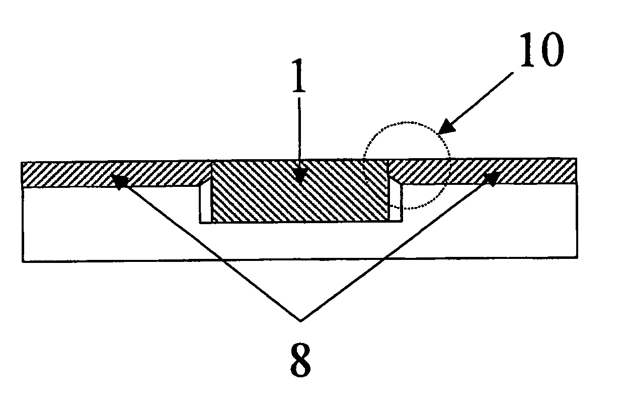
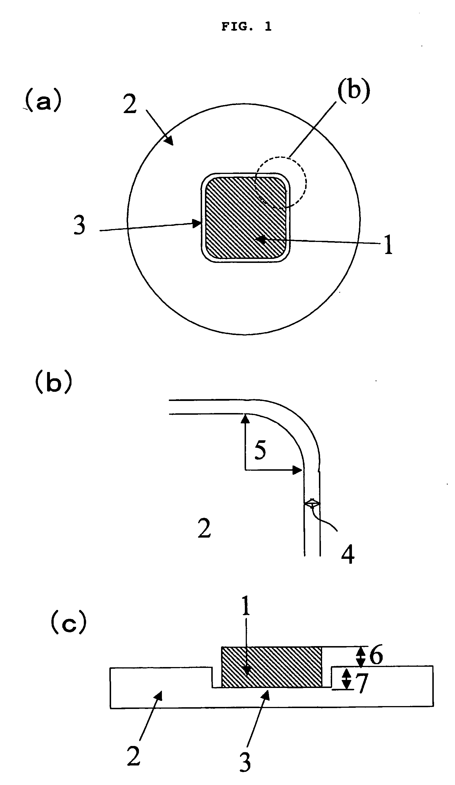
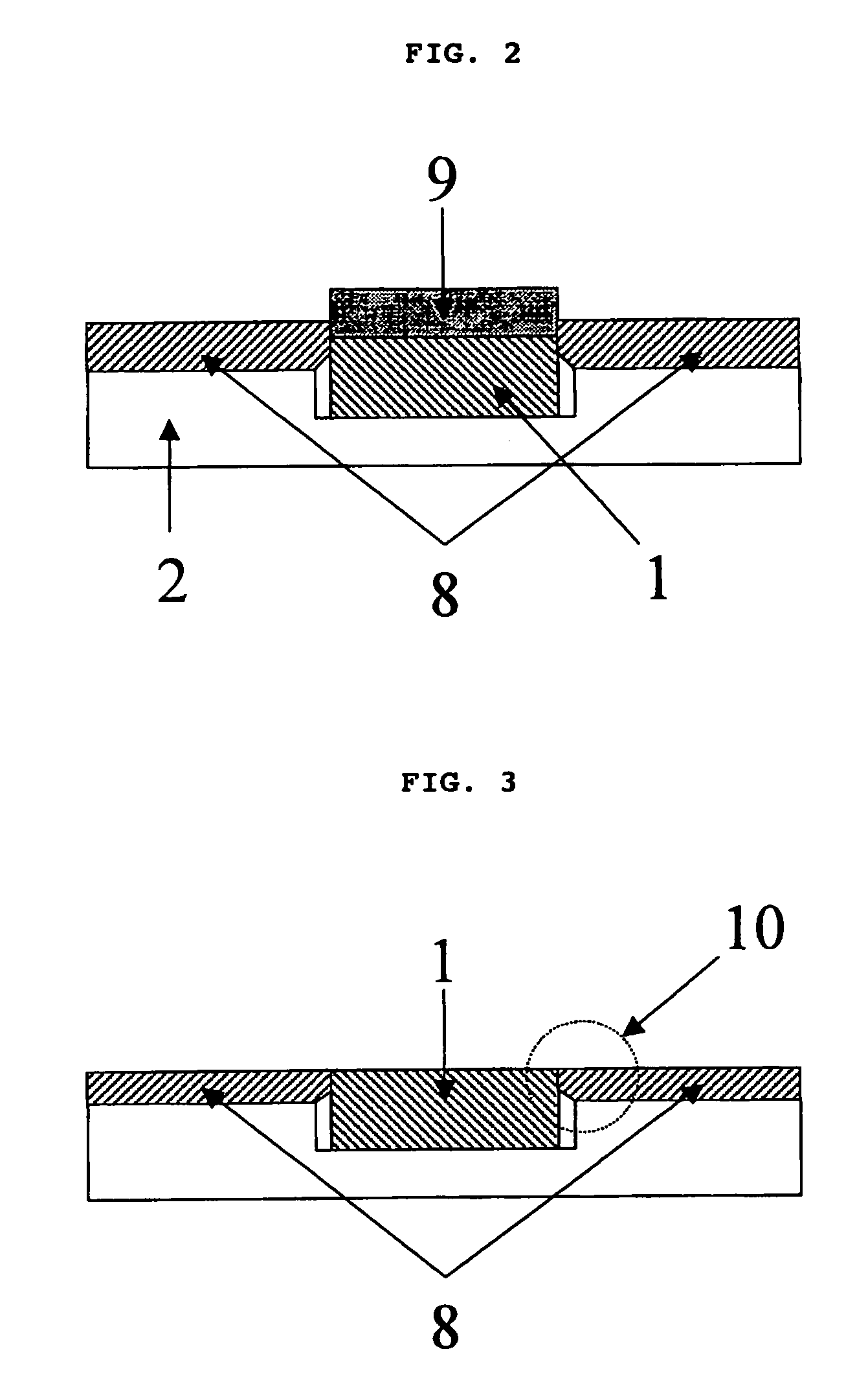
- A method involving a silicon substrate with a concave region for mounting a single crystalline diamond seed substrate, followed by chemical vapor deposition to form a CVD diamond layer, and subsequent mechanical polishing to unify and expose the single crystalline diamond seed substrate, ensuring strong bonding and high-quality crystallinity, while also allowing for conductive diamond substrates by using conductive materials.

Manufacturing Scalability Assessment
Manufacturing scalability represents a critical differentiator between diamond substrates and graphene technologies, with each material presenting distinct challenges and opportunities for large-scale production. The scalability assessment reveals fundamental differences in production methodologies, infrastructure requirements, and economic viability at industrial volumes.
Diamond substrate manufacturing relies primarily on Chemical Vapor Deposition (CVD) and High Pressure High Temperature (HPHT) synthesis methods. CVD processes, while offering superior control over crystal quality and doping characteristics, face significant scalability constraints due to lengthy deposition times ranging from hours to days for achieving desired thickness. The process requires specialized reactor chambers operating at temperatures exceeding 800°C with precise gas flow control, limiting throughput capacity. HPHT methods can produce larger volumes but struggle with uniformity control across batch sizes, creating quality consistency challenges at scale.
Graphene manufacturing demonstrates superior scalability potential through multiple production pathways. Chemical exfoliation and liquid-phase exfoliation techniques enable continuous processing with relatively simple equipment requirements. Roll-to-roll CVD processes have emerged as particularly promising for large-area graphene production, achieving substrate sizes exceeding several meters while maintaining reasonable production speeds. These methods leverage existing semiconductor manufacturing infrastructure, reducing capital investment barriers for scaling operations.
Infrastructure requirements differ substantially between the two materials. Diamond substrate production demands specialized high-temperature furnaces, ultra-pure gas handling systems, and extensive quality control equipment, resulting in capital expenditures often exceeding tens of millions of dollars for commercial-scale facilities. The energy consumption per unit area remains significantly higher due to extreme processing conditions and extended cycle times.
Graphene manufacturing infrastructure proves more adaptable and cost-effective for scaling. Existing chemical processing equipment can often be modified for graphene production, while roll-to-roll systems utilize proven manufacturing principles from the printing and coating industries. Energy requirements per unit area are substantially lower, and production cycle times measured in minutes rather than hours enable higher throughput rates.
Yield optimization presents ongoing challenges for both materials but with different characteristics. Diamond substrate yields are highly sensitive to process parameter variations, with defect formation significantly impacting usable output. Graphene production achieves higher overall yields but faces quality uniformity challenges across large areas, particularly regarding layer count control and electrical property consistency.
The scalability trajectory favors graphene for near-term commercial applications requiring large volumes, while diamond substrates remain constrained to specialized high-value applications where superior performance justifies higher production costs and longer lead times.
Diamond substrate manufacturing relies primarily on Chemical Vapor Deposition (CVD) and High Pressure High Temperature (HPHT) synthesis methods. CVD processes, while offering superior control over crystal quality and doping characteristics, face significant scalability constraints due to lengthy deposition times ranging from hours to days for achieving desired thickness. The process requires specialized reactor chambers operating at temperatures exceeding 800°C with precise gas flow control, limiting throughput capacity. HPHT methods can produce larger volumes but struggle with uniformity control across batch sizes, creating quality consistency challenges at scale.
Graphene manufacturing demonstrates superior scalability potential through multiple production pathways. Chemical exfoliation and liquid-phase exfoliation techniques enable continuous processing with relatively simple equipment requirements. Roll-to-roll CVD processes have emerged as particularly promising for large-area graphene production, achieving substrate sizes exceeding several meters while maintaining reasonable production speeds. These methods leverage existing semiconductor manufacturing infrastructure, reducing capital investment barriers for scaling operations.
Infrastructure requirements differ substantially between the two materials. Diamond substrate production demands specialized high-temperature furnaces, ultra-pure gas handling systems, and extensive quality control equipment, resulting in capital expenditures often exceeding tens of millions of dollars for commercial-scale facilities. The energy consumption per unit area remains significantly higher due to extreme processing conditions and extended cycle times.
Graphene manufacturing infrastructure proves more adaptable and cost-effective for scaling. Existing chemical processing equipment can often be modified for graphene production, while roll-to-roll systems utilize proven manufacturing principles from the printing and coating industries. Energy requirements per unit area are substantially lower, and production cycle times measured in minutes rather than hours enable higher throughput rates.
Yield optimization presents ongoing challenges for both materials but with different characteristics. Diamond substrate yields are highly sensitive to process parameter variations, with defect formation significantly impacting usable output. Graphene production achieves higher overall yields but faces quality uniformity challenges across large areas, particularly regarding layer count control and electrical property consistency.
The scalability trajectory favors graphene for near-term commercial applications requiring large volumes, while diamond substrates remain constrained to specialized high-value applications where superior performance justifies higher production costs and longer lead times.
Environmental Impact of Carbon Substrate Production
The production of carbon substrates, particularly diamond and graphene, presents significant environmental challenges that vary considerably between manufacturing processes. Diamond substrate production through chemical vapor deposition (CVD) requires extremely high temperatures ranging from 800-1200°C and substantial energy consumption, typically demanding 50-100 kWh per carat of synthetic diamond. This energy-intensive process generates considerable carbon emissions, especially when powered by fossil fuel-based electricity grids.
Graphene production methods exhibit diverse environmental footprints depending on the synthesis approach. Mechanical exfoliation, while producing high-quality graphene, generates substantial material waste with yields often below 1%. Chemical vapor deposition for graphene requires lower temperatures than diamond synthesis, typically 800-1000°C, but still demands significant energy input and often utilizes methane or other hydrocarbon precursors that contribute to greenhouse gas emissions.
The liquid-phase exfoliation method for graphene production involves organic solvents such as N-methyl-2-pyrrolidone (NMP) or dimethylformamide (DMF), which pose environmental risks through potential groundwater contamination and air quality degradation. Solvent recovery and recycling systems can mitigate these impacts but require additional energy investment and infrastructure.
Water consumption represents another critical environmental factor, particularly in diamond substrate production where cooling systems and chemical processing require substantial water resources. Graphene oxide production through the Hummers method generates acidic waste streams containing sulfuric acid and potassium permanganate, necessitating careful neutralization and disposal protocols.
Emerging production technologies show promise for reducing environmental impact. Plasma-enhanced CVD systems demonstrate improved energy efficiency for both diamond and graphene synthesis. Additionally, bio-based precursors and renewable energy integration in manufacturing facilities are beginning to address the carbon footprint concerns associated with substrate production.
The lifecycle assessment of carbon substrates must also consider end-of-life disposal and recycling potential. Diamond substrates offer superior durability and potential for reuse, while graphene's integration into composite materials may complicate recycling processes. Developing sustainable production pathways remains crucial for the widespread adoption of these advanced carbon materials in electronic applications.
Graphene production methods exhibit diverse environmental footprints depending on the synthesis approach. Mechanical exfoliation, while producing high-quality graphene, generates substantial material waste with yields often below 1%. Chemical vapor deposition for graphene requires lower temperatures than diamond synthesis, typically 800-1000°C, but still demands significant energy input and often utilizes methane or other hydrocarbon precursors that contribute to greenhouse gas emissions.
The liquid-phase exfoliation method for graphene production involves organic solvents such as N-methyl-2-pyrrolidone (NMP) or dimethylformamide (DMF), which pose environmental risks through potential groundwater contamination and air quality degradation. Solvent recovery and recycling systems can mitigate these impacts but require additional energy investment and infrastructure.
Water consumption represents another critical environmental factor, particularly in diamond substrate production where cooling systems and chemical processing require substantial water resources. Graphene oxide production through the Hummers method generates acidic waste streams containing sulfuric acid and potassium permanganate, necessitating careful neutralization and disposal protocols.
Emerging production technologies show promise for reducing environmental impact. Plasma-enhanced CVD systems demonstrate improved energy efficiency for both diamond and graphene synthesis. Additionally, bio-based precursors and renewable energy integration in manufacturing facilities are beginning to address the carbon footprint concerns associated with substrate production.
The lifecycle assessment of carbon substrates must also consider end-of-life disposal and recycling potential. Diamond substrates offer superior durability and potential for reuse, while graphene's integration into composite materials may complicate recycling processes. Developing sustainable production pathways remains crucial for the widespread adoption of these advanced carbon materials in electronic applications.
Unlock deeper insights with PatSnap Eureka Quick Research — get a full tech report to explore trends and direct your research. Try now!
Generate Your Research Report Instantly with AI Agent
Supercharge your innovation with PatSnap Eureka AI Agent Platform!