Microtransfer Printing vs Vapor Deposition: An Efficiency Guide
APR 23, 20269 MIN READ
Generate Your Research Report Instantly with AI Agent
PatSnap Eureka helps you evaluate technical feasibility & market potential.
Microtransfer Printing vs Vapor Deposition Background and Objectives
The semiconductor and display manufacturing industries have witnessed remarkable technological evolution over the past decades, driven by the relentless pursuit of miniaturization, enhanced performance, and cost-effective production methods. Two pivotal technologies have emerged as critical enablers in advanced device fabrication: microtransfer printing and vapor deposition. These technologies represent fundamentally different approaches to material placement and device assembly, each offering unique advantages and facing distinct challenges in modern manufacturing environments.
Microtransfer printing has evolved from traditional printing concepts into a sophisticated manufacturing technique capable of handling microscale components with exceptional precision. This technology enables the selective transfer of pre-fabricated micro-devices from donor substrates to receiver substrates, facilitating heterogeneous integration across different material systems. The technique has gained significant traction in applications requiring precise placement of discrete components, particularly in advanced display technologies and photonic devices.
Vapor deposition technologies, encompassing both physical vapor deposition (PVD) and chemical vapor deposition (CVD), have long served as cornerstone processes in semiconductor manufacturing. These techniques involve the formation of thin films through the condensation of vaporized materials onto substrates, enabling atomic-level control over material properties and thickness uniformity across large surface areas.
The primary objective of comparing these technologies centers on evaluating their respective efficiencies across multiple dimensions including throughput, material utilization, energy consumption, and process scalability. Understanding the efficiency trade-offs becomes crucial as manufacturers seek to optimize production costs while maintaining quality standards and meeting increasingly demanding performance specifications.
Current market demands for flexible electronics, micro-LED displays, and advanced packaging solutions have intensified the need for comprehensive efficiency analysis between these competing approaches. The comparison aims to identify optimal application domains for each technology, considering factors such as substrate compatibility, processing temperatures, material waste, and overall manufacturing complexity.
This technological assessment seeks to establish clear performance benchmarks and provide strategic insights for technology selection in next-generation manufacturing processes, ultimately supporting informed decision-making in capital equipment investments and process development initiatives.
Market Demand Analysis for Advanced Deposition Technologies
The global semiconductor and display manufacturing industries are experiencing unprecedented growth, driving substantial demand for advanced deposition technologies. This expansion is primarily fueled by the proliferation of consumer electronics, automotive electronics, and emerging applications in augmented reality, virtual reality, and flexible displays. Manufacturing facilities worldwide are seeking more efficient, cost-effective, and precise deposition methods to meet increasingly stringent performance requirements while maintaining competitive production costs.
Microtransfer printing technology addresses critical market needs in applications requiring heterogeneous integration and precise material placement. The technology demonstrates particular value in micro-LED display manufacturing, where traditional pick-and-place methods prove inadequate for handling millions of microscopic components. Market demand for micro-LED displays continues expanding across smartphone, television, and automotive display segments, creating substantial opportunities for microtransfer printing adoption.
Vapor deposition technologies maintain strong market positioning across multiple semiconductor and display manufacturing processes. Chemical vapor deposition and physical vapor deposition methods remain essential for thin-film formation, barrier layers, and metallization processes. The market demand spans from established applications in silicon-based semiconductors to emerging compound semiconductor devices used in 5G infrastructure and electric vehicle power electronics.
The flexible electronics market represents a convergence point where both technologies compete for market share. Manufacturers require deposition methods capable of processing temperature-sensitive substrates while maintaining material quality and production throughput. This market segment includes flexible displays, wearable electronics, and printed electronics applications, each presenting unique technical requirements and cost constraints.
Regional market dynamics reveal varying preferences for deposition technologies based on local manufacturing capabilities and target applications. Asian markets, particularly in South Korea, Taiwan, and China, demonstrate strong demand for both technologies driven by major display and semiconductor manufacturing investments. European and North American markets show increasing interest in specialized applications requiring precise material placement and novel device architectures.
The competitive landscape indicates growing market segmentation based on specific application requirements rather than universal technology adoption. Manufacturers increasingly evaluate deposition technologies based on total cost of ownership, including equipment costs, material utilization efficiency, processing speed, and yield considerations. This trend suggests sustained demand for both microtransfer printing and vapor deposition technologies, with market success determined by application-specific performance advantages rather than broad technological superiority.
Current Status and Challenges in Printing and Deposition Methods
Microtransfer printing and vapor deposition technologies represent two fundamentally different approaches to material deposition, each facing distinct technical and operational challenges in contemporary manufacturing environments. Both methods have evolved significantly over the past decade, yet continue to encounter limitations that affect their widespread adoption across various industrial applications.
Microtransfer printing currently struggles with scalability issues, particularly when transitioning from laboratory-scale demonstrations to industrial production volumes. The technology exhibits excellent precision for small-area applications but faces significant throughput limitations due to the sequential nature of the transfer process. Yield consistency remains a critical concern, with defect rates varying substantially based on substrate conditions, environmental factors, and the mechanical properties of transfer stamps. The technology also encounters material compatibility constraints, as not all semiconductor materials can be effectively processed using current elastomeric stamp materials.
Vapor deposition methods, while more mature, confront their own set of challenges related to material utilization efficiency and process uniformity. Chemical vapor deposition processes often suffer from poor precursor utilization rates, with significant material waste occurring during deposition cycles. Physical vapor deposition techniques face limitations in achieving uniform thickness distribution across large substrate areas, particularly for complex three-dimensional structures. Temperature requirements for many vapor deposition processes also restrict substrate material choices and can introduce thermal stress-related defects.
Both technologies encounter significant challenges in achieving cost-effective production at scale. Microtransfer printing requires expensive precision alignment equipment and specialized stamp materials that degrade over time, necessitating frequent replacement. Vapor deposition systems demand high-vacuum environments and precise temperature control, resulting in substantial energy consumption and maintenance costs.
Process integration represents another shared challenge, as both methods must be compatible with existing semiconductor fabrication workflows. Contamination control remains critical for both approaches, though the specific contamination sources and mitigation strategies differ significantly between the two technologies.
The geographical distribution of expertise and manufacturing capabilities varies considerably between these technologies. Vapor deposition infrastructure is well-established globally, with mature supply chains and standardized equipment. Microtransfer printing capabilities remain concentrated in specialized research institutions and a limited number of commercial facilities, creating potential bottlenecks for technology adoption and scaling.
Current Technical Solutions for Efficient Material Transfer
01 Microtransfer printing for OLED device fabrication
Microtransfer printing techniques enable efficient transfer of organic materials and functional layers onto substrates for OLED manufacturing. This method offers advantages in material utilization, pattern resolution, and reduced waste compared to traditional deposition methods. The process involves selective transfer of pre-patterned materials using elastomeric stamps or transfer media, allowing for precise placement and reduced material consumption.- Microtransfer printing for OLED device fabrication: Microtransfer printing techniques enable efficient transfer of organic materials and functional layers onto substrates for OLED manufacturing. This method offers advantages in material utilization, pattern resolution, and reduced waste compared to traditional deposition methods. The process involves transferring pre-formed patterns from donor substrates to receiver substrates with high precision and minimal material loss.
- Vapor deposition methods for thin film formation: Vapor deposition techniques including physical vapor deposition and chemical vapor deposition are widely used for creating uniform thin films in electronic devices. These methods provide controlled thickness, composition, and material properties. The efficiency of vapor deposition is characterized by deposition rate, material utilization ratio, and uniformity across large substrate areas.
- Material utilization efficiency comparison: Comparative analysis of material consumption and waste generation between different deposition methods reveals significant differences in efficiency metrics. Transfer printing methods can achieve higher material utilization rates by selective patterning and precise placement, while vapor deposition may result in material loss on chamber walls and masks. Economic and environmental considerations favor methods with minimal material waste.
- Throughput and scalability considerations: Production throughput and scalability to large-area substrates are critical factors in manufacturing efficiency. Different deposition technologies exhibit varying capabilities for batch processing, continuous operation, and adaptation to industrial-scale production. Process speed, substrate size limitations, and equipment complexity impact overall manufacturing efficiency and cost-effectiveness.
- Hybrid approaches combining multiple deposition techniques: Integration of microtransfer printing with vapor deposition methods enables optimization of manufacturing processes by leveraging advantages of each technique. Hybrid approaches can achieve superior pattern quality, material efficiency, and device performance. Sequential or parallel application of different deposition methods allows for complex multilayer structures with optimized properties for each functional layer.
02 Vapor deposition methods for thin film formation
Vapor deposition techniques including physical vapor deposition and chemical vapor deposition are widely used for creating uniform thin films in electronic devices. These methods provide controlled thickness, composition, and coverage across large substrate areas. The efficiency of vapor deposition is characterized by deposition rate, material utilization ratio, and uniformity of the deposited layers.Expand Specific Solutions03 Material utilization efficiency comparison
The efficiency of material usage differs significantly between printing and deposition methods. Transfer printing techniques can achieve higher material utilization rates by selectively placing materials only where needed, while vapor deposition methods may result in material waste on chamber walls and fixtures. Comparative studies evaluate the percentage of source material that reaches the target substrate versus material lost during processing.Expand Specific Solutions04 Throughput and scalability considerations
Manufacturing throughput and scalability vary between microtransfer printing and vapor deposition approaches. Printing methods may offer advantages in parallel processing and faster cycle times for certain applications, while vapor deposition can provide continuous processing capabilities. The choice between methods depends on production volume requirements, substrate size, and desired manufacturing speed.Expand Specific Solutions05 Hybrid approaches combining printing and deposition
Advanced manufacturing strategies integrate both microtransfer printing and vapor deposition techniques to optimize efficiency and device performance. Hybrid processes leverage the strengths of each method, using printing for selective patterning and deposition for conformal coating or encapsulation layers. These combined approaches can improve overall manufacturing efficiency while maintaining high quality standards.Expand Specific Solutions
Major Players in Microtransfer and Vapor Deposition Industries
The efficiency comparison between microtransfer printing and vapor deposition technologies represents a rapidly evolving competitive landscape within the semiconductor and display manufacturing industry. The market is currently in a growth phase, driven by increasing demand for advanced displays and miniaturized electronics, with significant market expansion expected in OLED and microLED applications. Technology maturity varies considerably across players, with established companies like ASM International NV and Advanced Micro Fabrication Equipment demonstrating mature vapor deposition capabilities, while Kateeva leads in innovative inkjet printing solutions for OLED production. Research institutions including South China University of Technology and Northwestern Polytechnical University are advancing fundamental research, while companies like Semiconductor Energy Laboratory and SPTS Technologies are developing hybrid approaches. The competitive dynamics show traditional vapor deposition maintaining dominance in established applications, while microtransfer printing gains traction in emerging flexible and large-area electronics markets.
Kateeva, Inc.
Technical Solution: Kateeva specializes in advanced inkjet printing technology for OLED manufacturing, offering an alternative approach to traditional vapor deposition methods. Their YIELDjet platform utilizes precision inkjet printing to deposit organic materials with high accuracy and material efficiency. This microtransfer printing approach enables selective material deposition with reduced waste compared to conventional vapor deposition techniques. The technology allows for room temperature processing and eliminates the need for shadow masks, potentially reducing manufacturing complexity. Kateeva's system demonstrates improved material utilization rates and enables flexible substrate processing, making it particularly suitable for large-area display manufacturing where traditional vapor deposition faces scalability challenges.
Strengths: Higher material utilization efficiency, room temperature processing, maskless deposition. Weaknesses: Limited to specific organic materials, potential resolution constraints compared to vapor deposition.
Seiko Epson Corp.
Technical Solution: Seiko Epson leverages its inkjet printing expertise to develop microtransfer printing solutions for electronic device manufacturing, particularly in the display and printed electronics sectors. Their technology enables precise deposition of functional materials including conductive inks, organic semiconductors, and dielectric materials with micron-level accuracy. Epson's approach emphasizes material efficiency and waste reduction compared to traditional vapor deposition methods. Their systems can operate at ambient conditions and offer flexibility in substrate selection, including flexible and curved surfaces. The company's research demonstrates that their microtransfer printing technology achieves comparable electrical performance to vapor-deposited films while offering significant advantages in material utilization and processing versatility for certain applications.
Strengths: High material efficiency, ambient processing conditions, substrate flexibility, proven inkjet technology base. Weaknesses: Limited material compatibility, potential resolution limitations for finest features.
Core Technology Analysis of Printing vs Deposition Efficiency
Deposition source, deposition device, and deposition film manufacturing method
PatentWO2017051790A1
Innovation
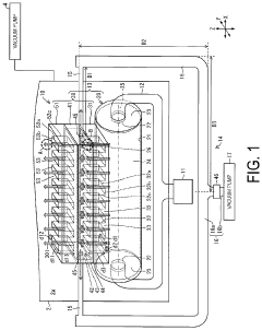
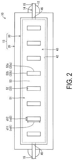
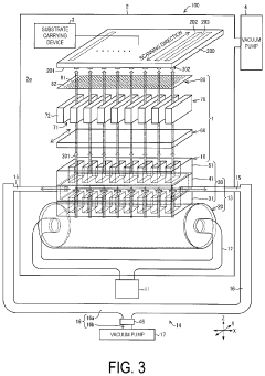
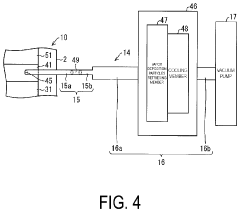
- The vapor deposition apparatus incorporates a plurality of vertically stacked evaporation nozzle sections with spaced nozzles, a vacuum pump, and a vacuum evacuation unit, where the pressure inside the vapor deposition nozzle sections is controlled to be lower upstream and higher downstream in the injection direction, reducing particle scattering and enhancing directional control of vapor deposition particles.


Vapor deposition source and vapor deposition device for producing vapor deposition film with high material usage efficiency
PatentActiveUS10760155B2
Innovation
- A vapor deposition source with multistage nozzle portions and a vacuum exhaust unit connected to spaces between the nozzles, adjusting pressure to ensure vapor deposition particles are emitted with higher directivity, reducing scattering and improving material usage efficiency.
Manufacturing Cost Analysis and Economic Feasibility
The manufacturing cost structure of microtransfer printing differs significantly from vapor deposition technologies, primarily due to equipment requirements and operational parameters. Microtransfer printing systems typically require lower capital investment compared to high-end vapor deposition equipment, particularly when considering molecular beam epitaxy or metal-organic chemical vapor deposition systems. The initial equipment cost for microtransfer printing ranges from $500,000 to $2 million, while advanced vapor deposition systems can exceed $5 million for industrial-scale operations.
Material utilization efficiency represents a critical cost factor distinguishing these technologies. Microtransfer printing achieves material utilization rates of 85-95% due to its selective transfer mechanism, minimizing waste of expensive semiconductor materials. In contrast, vapor deposition processes typically exhibit 30-60% material utilization efficiency, as significant portions of precursor materials are deposited on chamber walls or exhausted through vacuum systems.
Operational expenditure analysis reveals contrasting cost profiles between the technologies. Microtransfer printing operates at atmospheric pressure with minimal energy consumption, resulting in lower utility costs. The process requires specialized elastomeric stamps and donor substrates, contributing to recurring material costs of approximately $0.50-2.00 per device. Vapor deposition processes demand high-vacuum environments and elevated temperatures, leading to substantial energy consumption and maintenance requirements.
Throughput considerations significantly impact per-unit manufacturing costs. Microtransfer printing enables parallel processing of multiple devices simultaneously, achieving throughput rates of 100-1000 devices per hour depending on device complexity. Vapor deposition processes typically operate sequentially, with throughput rates of 10-100 wafers per hour, though each wafer may contain thousands of devices.
Economic feasibility assessment indicates that microtransfer printing becomes cost-competitive for production volumes exceeding 10,000 units annually, particularly for heterogeneous integration applications. The technology demonstrates superior economics for small-to-medium scale production due to lower fixed costs and higher material efficiency. Vapor deposition maintains advantages in high-volume manufacturing scenarios where amortization of capital equipment costs becomes favorable, typically above 100,000 units annually.
The total cost of ownership analysis over a five-year period shows microtransfer printing achieving 20-40% lower costs for specialized applications requiring precise material placement and minimal waste generation.
Environmental Impact Assessment of Deposition Technologies
The environmental implications of microtransfer printing and vapor deposition technologies present distinct profiles that significantly influence their adoption in manufacturing processes. Both technologies demonstrate varying degrees of environmental impact across multiple dimensions, from resource consumption to waste generation patterns.
Microtransfer printing exhibits a relatively favorable environmental footprint due to its additive manufacturing nature. The process generates minimal material waste since it precisely places materials only where needed, eliminating the excess material removal typical in subtractive processes. Energy consumption remains moderate as the technology operates at lower temperatures compared to traditional vapor deposition methods. The process typically requires minimal use of hazardous chemicals, reducing the risk of toxic emissions and simplifying waste management protocols.
Vapor deposition technologies, particularly chemical vapor deposition (CVD) and physical vapor deposition (PVD), present more complex environmental challenges. These processes often require high-temperature operations, resulting in substantial energy consumption and associated carbon emissions. The use of precursor gases and chemicals in CVD processes can generate hazardous byproducts requiring specialized treatment and disposal systems. Additionally, the vacuum requirements for many vapor deposition techniques contribute to increased energy demands.
Water usage patterns differ significantly between the two technologies. Microtransfer printing generally requires minimal water consumption, primarily for cleaning processes. Vapor deposition systems, however, often necessitate extensive cooling water circulation and chemical processing steps that increase overall water consumption and potential contamination risks.
The lifecycle assessment reveals that microtransfer printing demonstrates superior sustainability metrics in terms of material efficiency and waste reduction. However, vapor deposition technologies benefit from established recycling infrastructure for certain materials and byproducts. The scalability factor also influences environmental impact, as vapor deposition processes can achieve higher throughput rates, potentially offsetting per-unit environmental costs in large-scale manufacturing scenarios.
Regulatory compliance requirements vary substantially between these technologies, with vapor deposition facing stricter environmental controls due to potential emissions and chemical handling requirements, while microtransfer printing generally encounters fewer regulatory barriers related to environmental protection.
Unlock deeper insights with PatSnap Eureka Quick Research — get a full tech report to explore trends and direct your research. Try now!
Generate Your Research Report Instantly with AI Agent
Supercharge your innovation with PatSnap Eureka AI Agent Platform!