

Microtransfer Printing for Hypersensitive Sensor Assembly
APR 23, 20269 MIN READ
Generate Your Research Report Instantly with AI Agent
PatSnap Eureka helps you evaluate technical feasibility & market potential.
Microtransfer Printing Technology Background and Objectives
Microtransfer printing has emerged as a revolutionary manufacturing technique that enables the precise placement of microscale and nanoscale materials onto diverse substrates with exceptional accuracy. This technology represents a paradigm shift from traditional semiconductor manufacturing processes, offering unprecedented flexibility in heterogeneous integration of materials that would otherwise be incompatible through conventional fabrication methods.
The fundamental principle of microtransfer printing involves the use of elastomeric stamps to selectively retrieve microscale components from donor substrates and deposit them onto receiver substrates. This process leverages controlled adhesion mechanisms, where the interfacial adhesion between the stamp and the target material can be modulated through kinetic control, enabling selective pickup and release operations.
In the context of hypersensitive sensor assembly, microtransfer printing addresses critical limitations of conventional sensor fabrication approaches. Traditional methods often require high-temperature processing, chemical treatments, or lithographic processes that can compromise the sensitivity and functionality of delicate sensing elements. The gentle, room-temperature nature of microtransfer printing preserves the intrinsic properties of sensitive materials while enabling their integration into complex sensor architectures.
The technology has evolved significantly since its inception in the early 2000s, progressing from simple proof-of-concept demonstrations to sophisticated manufacturing platforms capable of handling diverse material systems. Key developments include advances in stamp materials, surface chemistry control, and automation systems that have enhanced throughput and reliability.
The primary objective of applying microtransfer printing to hypersensitive sensor assembly is to achieve deterministic placement of sensing elements with nanometer-scale precision while maintaining their functional integrity. This includes the ability to integrate heterogeneous materials such as quantum dots, nanowires, organic semiconductors, and biological components into unified sensor platforms without thermal or chemical degradation.
Furthermore, the technology aims to enable the fabrication of sensor arrays with unprecedented density and uniformity, facilitating the development of next-generation sensing systems for applications ranging from biomedical diagnostics to environmental monitoring. The ultimate goal is to establish a scalable manufacturing pathway that can transition from laboratory demonstrations to industrial-scale production of advanced sensor technologies.
Market Demand for Hypersensitive Sensor Applications
The global hypersensitive sensor market is experiencing unprecedented growth driven by the convergence of multiple technological and societal trends. Healthcare applications represent the largest segment, where hypersensitive sensors enable early disease detection, continuous patient monitoring, and personalized medicine approaches. The demand for wearable health devices capable of detecting minute biological markers, such as glucose levels, cardiac biomarkers, and inflammatory proteins, has intensified following increased health consciousness and aging populations worldwide.
Environmental monitoring applications constitute another significant demand driver, particularly in air quality assessment, water contamination detection, and industrial emission monitoring. Regulatory pressures for environmental compliance and growing public awareness of pollution-related health risks have accelerated adoption of hypersensitive sensor technologies capable of detecting trace-level contaminants and toxic substances.
The automotive industry presents substantial opportunities for hypersensitive sensors in advanced driver assistance systems and autonomous vehicle development. These applications require sensors with exceptional sensitivity for obstacle detection, environmental perception, and safety-critical decision making. The transition toward electric vehicles has further expanded demand for battery monitoring sensors that can detect early signs of thermal runaway and performance degradation.
Industrial Internet of Things applications drive demand for hypersensitive sensors in predictive maintenance, process optimization, and quality control. Manufacturing facilities increasingly rely on sensors capable of detecting minute changes in vibration, temperature, chemical composition, and structural integrity to prevent costly equipment failures and maintain product quality standards.
Consumer electronics applications, including smartphones, smart home devices, and augmented reality systems, require miniaturized hypersensitive sensors for gesture recognition, biometric authentication, and environmental adaptation. The proliferation of smart devices has created substantial volume demand for cost-effective, high-performance sensor solutions.
Defense and security applications represent a specialized but high-value market segment, where hypersensitive sensors enable chemical threat detection, surveillance systems, and communication security. Government investments in homeland security and military modernization programs continue to drive demand for advanced sensor technologies with superior sensitivity and reliability characteristics.
Current State and Challenges in Microtransfer Printing
Microtransfer printing has emerged as a critical enabling technology for advanced sensor assembly, particularly in applications requiring hypersensitive detection capabilities. Currently, the technology demonstrates significant potential in transferring microscale and nanoscale functional materials with high precision, enabling the fabrication of sensors with enhanced sensitivity and miniaturized form factors. Leading research institutions and semiconductor companies have successfully demonstrated microtransfer printing for various sensor components, including photodetectors, chemical sensors, and biosensors.
The precision achievable in current microtransfer printing systems ranges from sub-micrometer to several micrometers, depending on the specific technique employed. Elastomeric stamp-based approaches dominate the field, utilizing polydimethylsiloxane (PDMS) and other polymer materials to facilitate controlled transfer of device structures. These systems can handle diverse material types, including III-V semiconductors, two-dimensional materials, and organic compounds essential for sensor functionality.
Despite technological advances, several critical challenges persist in microtransfer printing for hypersensitive sensor applications. Adhesion control remains a fundamental obstacle, as achieving reliable pickup and release of microscale components requires precise manipulation of interfacial forces. The balance between sufficient adhesion for stable transfer and controlled release at target locations continues to limit throughput and yield in manufacturing environments.
Alignment accuracy presents another significant challenge, particularly when assembling multi-component sensor systems requiring nanometer-scale precision. Current alignment systems struggle to maintain consistent positioning across large substrate areas, leading to performance variations in sensor arrays. Temperature fluctuations, mechanical vibrations, and substrate deformation contribute to alignment drift during the transfer process.
Material compatibility issues further complicate the implementation of microtransfer printing in sensor assembly. Different materials exhibit varying surface energies and mechanical properties, requiring customized transfer protocols for each component type. This complexity increases process development time and limits the versatility of manufacturing platforms.
Contamination control represents a critical concern in hypersensitive sensor fabrication, where even trace amounts of foreign materials can significantly impact device performance. Current microtransfer printing processes face challenges in maintaining clean interfaces throughout the transfer sequence, particularly when handling multiple material systems sequentially.
Scalability limitations constrain the commercial viability of microtransfer printing for large-scale sensor production. While laboratory demonstrations show promising results for individual devices or small arrays, scaling to wafer-level processing with consistent quality and throughput remains challenging. Process uniformity across large areas and integration with existing semiconductor manufacturing infrastructure require substantial technological development.
Current Microtransfer Printing Solutions
01 Ink composition optimization for enhanced sensitivity
The sensitivity of microtransfer printing can be improved by optimizing the ink composition, including the selection of appropriate pigments, binders, and additives. The formulation affects the transfer efficiency and print quality by controlling viscosity, surface tension, and adhesion properties. Specific ratios of components and the inclusion of sensitizing agents can enhance the responsiveness of the ink to transfer conditions.- Ink composition optimization for enhanced sensitivity: The sensitivity of microtransfer printing can be improved by optimizing the ink composition, including the selection of appropriate pigments, binders, and additives. The formulation affects the transfer efficiency and print quality by controlling viscosity, surface tension, and adhesion properties. Specific ratios of components and the inclusion of sensitizing agents can enhance the responsiveness of the ink to transfer conditions.
- Substrate surface treatment and modification: Surface treatment of the receiving substrate plays a crucial role in improving microtransfer printing sensitivity. Methods include plasma treatment, chemical modification, and coating with receptor layers to enhance ink adhesion and transfer efficiency. The surface energy and roughness of the substrate can be adjusted to optimize the interaction between the transferred material and the receiving surface.
- Transfer stamp material and structure design: The material properties and structural design of the transfer stamp significantly affect printing sensitivity. Elastomeric materials with specific hardness, surface patterns, and micro-structured features can improve contact uniformity and release characteristics. The stamp geometry and compliance can be engineered to achieve better conformability to substrate surfaces and more precise pattern transfer.
- Process parameter control and optimization: Controlling process parameters such as transfer pressure, temperature, contact time, and separation speed is essential for achieving high sensitivity in microtransfer printing. Precise control of these parameters enables consistent transfer of fine features and improves reproducibility. Dynamic adjustment of conditions during the transfer process can compensate for variations in material properties and environmental factors.
- Pattern resolution and registration accuracy enhancement: Improving the sensitivity of microtransfer printing involves enhancing pattern resolution and registration accuracy through advanced alignment systems and high-precision positioning mechanisms. Optical detection methods and feedback control systems can be employed to ensure accurate placement of transferred patterns. The use of specialized imaging techniques and measurement tools enables real-time monitoring and adjustment of the printing process.
02 Substrate surface treatment and modification
Treating and modifying the substrate surface can significantly improve microtransfer printing sensitivity. Surface treatments such as plasma treatment, chemical modification, or coating with specific materials can enhance ink adhesion and transfer efficiency. The surface energy and roughness of the substrate play crucial roles in determining the quality and sensitivity of the printing process.Expand Specific Solutions03 Transfer pressure and temperature control
Precise control of transfer pressure and temperature is essential for achieving optimal microtransfer printing sensitivity. The application of appropriate pressure ensures complete contact between the donor and receptor surfaces, while temperature control affects the rheological properties of the ink and the bonding strength. Dynamic adjustment of these parameters during the transfer process can enhance printing resolution and consistency.Expand Specific Solutions04 Stamp material and structure design
The material selection and structural design of the transfer stamp directly impact printing sensitivity. Elastomeric materials with specific hardness and surface properties enable conformal contact and efficient ink transfer. Microstructured or patterned stamp surfaces can improve transfer selectivity and resolution. The stamp's mechanical properties, including elasticity and durability, are critical factors in maintaining consistent printing performance.Expand Specific Solutions05 Drying and curing process optimization
The drying and curing processes following microtransfer printing significantly affect the final print sensitivity and quality. Controlled drying conditions, including temperature, humidity, and air flow, prevent defects such as cracking or uneven coating. Curing methods such as UV exposure, thermal treatment, or chemical crosslinking can enhance the adhesion and durability of the transferred material. Optimization of these post-transfer processes ensures stable and reproducible printing results.Expand Specific Solutions
Key Players in Microtransfer Printing Industry
The microtransfer printing technology for hypersensitive sensor assembly represents an emerging field in the early commercialization stage, with significant growth potential driven by increasing demand for miniaturized, high-performance sensors across healthcare, electronics, and industrial applications. The market demonstrates moderate maturity with established academic foundations but limited commercial deployment. Technology maturity varies significantly among key players: X Display Co. Technology Ltd. leads with commercialized μTP platforms, while research institutions like University of Illinois, Huazhong University of Science & Technology, and SINANO advance fundamental research. Industrial giants Robert Bosch GmbH and FUJIFILM Corp. represent potential large-scale adopters, whereas specialized companies like NanoInk Inc. and DB HITEK Co. focus on niche applications. The competitive landscape shows a clear divide between technology developers and end-users, with academic institutions bridging research gaps and companies like IMEC facilitating technology transfer, indicating a maturing ecosystem poised for broader commercial adoption.
The Board of Trustees of the University of Illinois
Technical Solution: Developed pioneering microtransfer printing technology using elastomeric stamps for precise assembly of microscale materials onto target substrates. Their approach enables selective pickup and placement of semiconductor devices with sub-micron accuracy, particularly effective for heterogeneous integration of different material systems. The technology utilizes kinetically controlled adhesion mechanisms and surface energy modulation to achieve high-yield transfer processes. Their research demonstrates successful integration of III-V semiconductors onto silicon substrates for advanced sensor applications, with transfer yields exceeding 95% for devices ranging from 1-100 micrometers in size.
Strengths: Pioneer in the field with extensive patent portfolio and proven scalability. Weaknesses: Limited commercial manufacturing experience and potential licensing complexities.
Robert Bosch GmbH
Technical Solution: Implements microtransfer printing for MEMS sensor manufacturing, focusing on high-precision assembly of pressure and inertial sensors. Their approach combines traditional semiconductor processing with selective transfer techniques to create multi-functional sensor arrays. The technology enables integration of different sensing elements onto single substrates, reducing package size while improving sensitivity. Bosch's process achieves positioning accuracy within ±0.5 micrometers and supports batch processing for cost-effective manufacturing. Their hypersensitive sensor assemblies demonstrate enhanced signal-to-noise ratios through optimized material interfaces and reduced parasitic effects.
Strengths: Strong manufacturing capabilities and established market presence in automotive sensors. Weaknesses: Focus primarily on specific sensor types may limit broader applications.
Core Patents in Hypersensitive Sensor Assembly
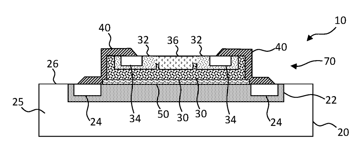
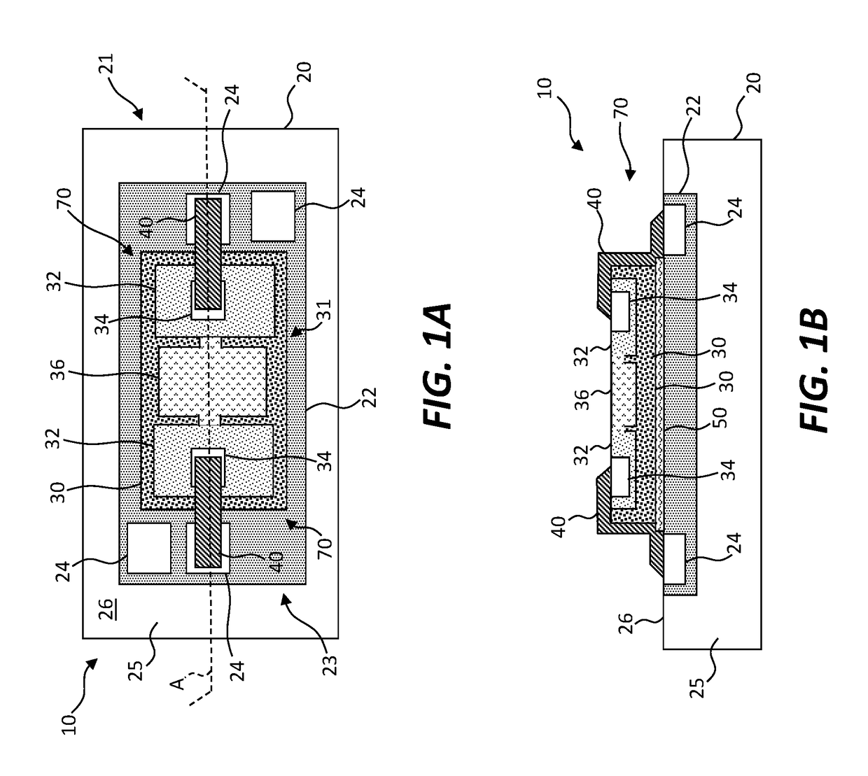
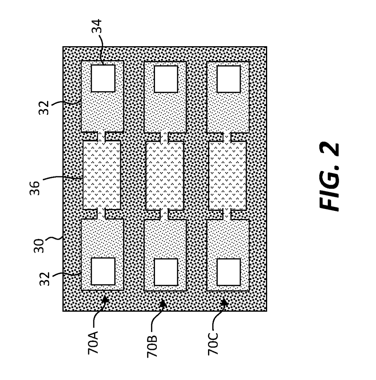
Micro-transfer printing methods
PatentPendingUS20250210399A1
Innovation
- A method involving a visco-elastic stamp with controlled horizontal and vertical movements, including rotations, is used to detach micro-components from a source wafer by fracturing or separating the tether, utilizing a motion-control platform for precise alignment and stress concentration on the tether to facilitate detachment.


Micro-transfer-printed compound sensor device
PatentActiveUS20170225945A1
Innovation
- A compound sensor device is created by micro-transfer printing a sensor substrate with a different material and technology onto a semiconductor substrate, reducing the length of electrical connections and enabling better integration and performance, particularly in high-frequency applications.

Manufacturing Standards for Microsensor Assembly
The establishment of comprehensive manufacturing standards for microsensor assembly represents a critical foundation for advancing microtransfer printing technologies in hypersensitive sensor applications. Current industry practices reveal significant variations in assembly protocols, dimensional tolerances, and quality control measures across different manufacturers and research institutions. This inconsistency creates substantial barriers to scalable production and reliable performance validation of hypersensitive sensors.
Dimensional precision standards constitute the primary framework for microsensor assembly manufacturing. Industry-leading specifications typically require positional accuracy within ±0.5 micrometers for sensor element placement, with surface roughness parameters maintained below 10 nanometers Ra. These stringent requirements necessitate specialized metrology equipment and controlled environmental conditions, including temperature stability within ±0.1°C and vibration isolation systems capable of attenuating disturbances below 1 micrometer amplitude.
Material compatibility standards address the critical interface requirements between sensor substrates, transfer media, and target assemblies. Established protocols mandate comprehensive characterization of thermal expansion coefficients, surface energy properties, and chemical compatibility matrices. These standards ensure reliable adhesion mechanisms while preventing contamination or degradation during the transfer printing process.
Process control standards encompass critical parameters including transfer pressure profiles, temperature cycling protocols, and timing sequences. Validated manufacturing procedures typically specify pressure application rates between 0.1-1.0 MPa/second, with dwell times optimized for specific material combinations. Temperature control protocols maintain substrate temperatures within ±2°C during critical transfer phases.
Quality assurance frameworks integrate real-time monitoring systems with post-assembly validation procedures. Standard protocols require electrical continuity testing, optical inspection at sub-micrometer resolution, and mechanical stress testing under accelerated aging conditions. These comprehensive validation procedures ensure consistent performance characteristics and long-term reliability of assembled hypersensitive sensor systems.
Contamination control standards establish cleanroom requirements, typically Class 100 or better environments, with specific protocols for handling procedures, storage conditions, and equipment maintenance schedules to maintain assembly integrity throughout the manufacturing process.
Quality Control in Microtransfer Printing Processes
Quality control in microtransfer printing processes represents a critical aspect of manufacturing hypersensitive sensors, where precision and reliability directly impact sensor performance. The inherently small scale of microtransfer printing operations, typically involving features ranging from micrometers to millimeters, demands sophisticated monitoring and control mechanisms to ensure consistent output quality.
The primary quality control challenges stem from the multi-step nature of microtransfer printing, which includes donor substrate preparation, pick-up operations, transport phases, and final placement onto receiver substrates. Each stage introduces potential sources of variation that can compromise the integrity of sensor assemblies. Critical parameters requiring continuous monitoring include transfer yield, positional accuracy, material integrity, and interface quality between transferred elements and target substrates.
Real-time monitoring systems have emerged as essential tools for maintaining process control. Advanced optical inspection techniques, including high-resolution microscopy and automated defect detection algorithms, enable immediate identification of transfer failures, misalignments, or material defects. These systems typically integrate machine learning capabilities to distinguish between acceptable variations and critical deviations that could affect sensor sensitivity.
Statistical process control methodologies play a crucial role in establishing acceptable quality thresholds and identifying process drift before it impacts production outcomes. Control charts tracking key metrics such as transfer success rates, dimensional accuracy, and electrical continuity provide operators with actionable insights for process optimization. The implementation of Design of Experiments approaches helps identify optimal parameter combinations while minimizing quality variations.
Environmental control represents another fundamental aspect of quality assurance in microtransfer printing. Temperature fluctuations, humidity variations, and particulate contamination can significantly impact transfer reliability and material properties. Cleanroom environments with precise climate control and continuous monitoring of atmospheric conditions are typically required to maintain consistent process performance.
Traceability systems enable comprehensive quality documentation throughout the manufacturing process, linking individual sensor assemblies to specific process parameters and material batches. This capability proves essential for identifying root causes of quality issues and implementing corrective actions. Integration with manufacturing execution systems provides real-time visibility into process performance and facilitates rapid response to quality deviations.
Unlock deeper insights with PatSnap Eureka Quick Research — get a full tech report to explore trends and direct your research. Try now!
Generate Your Research Report Instantly with AI Agent
Supercharge your innovation with PatSnap Eureka AI Agent Platform!