

Enhance Magnetoelectric Material Interaction with Substrates
APR 16, 20269 MIN READ
Generate Your Research Report Instantly with AI Agent
PatSnap Eureka helps you evaluate technical feasibility & market potential.
Magnetoelectric Material Development Background and Objectives
Magnetoelectric materials represent a fascinating class of multifunctional materials that exhibit coupled magnetic and electric properties, enabling direct conversion between magnetic and electric fields. This coupling phenomenon has garnered significant attention in the scientific community due to its potential applications in next-generation electronic devices, sensors, actuators, and memory storage systems. The fundamental principle underlying magnetoelectric effects involves the interaction between magnetic and electric order parameters within a single material or composite system.
The historical development of magnetoelectric materials traces back to the 1960s when Pierre Curie first predicted the theoretical possibility of magnetoelectric coupling. However, practical applications remained limited due to weak coupling effects in single-phase materials at room temperature. The field experienced renewed interest in the 1990s with the discovery of strong magnetoelectric effects in composite materials and the identification of multiferroic compounds that simultaneously exhibit ferroelectric and ferromagnetic properties.
Current technological evolution focuses on enhancing the magnetoelectric coefficient, which quantifies the strength of coupling between magnetic and electric fields. Researchers have explored various approaches including layered composites, particulate composites, and single-phase multiferroic materials. The substrate interaction plays a crucial role in determining the overall performance, as it influences strain transfer, interfacial coupling, and thermal stability of the magnetoelectric response.
The primary technical objectives center on achieving robust magnetoelectric coupling at room temperature with enhanced sensitivity and reduced power consumption. Key targets include developing materials with magnetoelectric coefficients exceeding 100 V/cm·Oe, improving frequency response characteristics for high-speed applications, and establishing reliable substrate integration methods that maintain coupling efficiency across temperature variations.
Strategic goals encompass creating scalable manufacturing processes for industrial applications, particularly in magnetic field sensors, energy harvesting devices, and spintronic components. The ultimate vision involves realizing voltage-controlled magnetic devices that could revolutionize data storage and processing technologies while significantly reducing energy consumption compared to current electromagnetic systems.
Market Demand for Enhanced Substrate-Material Interfaces
The global electronics industry is experiencing unprecedented demand for advanced magnetoelectric materials with enhanced substrate interactions, driven by the rapid expansion of Internet of Things devices, wearable electronics, and next-generation computing systems. This surge reflects the critical need for materials that can efficiently convert between magnetic and electric energy while maintaining strong interfacial bonding with various substrate materials.
Automotive electronics represents one of the fastest-growing market segments demanding improved magnetoelectric-substrate interfaces. Electric vehicle manufacturers require sensors and actuators that can withstand extreme temperature variations and mechanical stress while maintaining precise magnetic field detection capabilities. The integration of these materials with silicon carbide and gallium nitride substrates has become essential for power management systems and motor control applications.
The telecommunications sector is driving substantial demand for magnetoelectric materials that can interface effectively with flexible substrates. Fifth-generation wireless infrastructure requires components that combine magnetic sensing capabilities with mechanical flexibility, necessitating advanced interfacial engineering between magnetoelectric films and polymer or ceramic substrates. This application area particularly values materials that maintain performance integrity under repeated mechanical deformation.
Healthcare and biomedical device markets are emerging as significant consumers of enhanced magnetoelectric-substrate systems. Implantable medical devices and non-invasive diagnostic equipment require biocompatible interfaces that can function reliably in physiological environments. The demand centers on materials that can bond effectively with biocompatible substrates while providing stable magnetoelectric responses for therapeutic and monitoring applications.
Consumer electronics manufacturers are increasingly seeking magnetoelectric materials with superior substrate adhesion for miniaturized devices. Smartphone manufacturers and wearable device producers require materials that can maintain functionality despite the mechanical stresses associated with thin-form-factor designs. The market particularly values solutions that enable reliable performance across diverse substrate materials including glass, ceramics, and advanced polymers.
Industrial automation and robotics sectors are generating growing demand for robust magnetoelectric-substrate interfaces capable of operating in harsh environments. Manufacturing equipment requires sensors that can maintain calibration accuracy despite exposure to vibration, temperature cycling, and chemical exposure, driving the need for enhanced interfacial stability between magnetoelectric materials and industrial-grade substrates.
Current Challenges in Magnetoelectric-Substrate Interactions
Magnetoelectric materials face significant substrate-related challenges that fundamentally limit their performance and practical applications. The primary obstacle stems from lattice mismatch between magnetoelectric thin films and their substrates, which introduces structural defects, strain-induced distortions, and compromised functional properties. This mismatch creates dislocations and grain boundaries that act as scattering centers for charge carriers and magnetic domains, ultimately degrading the magnetoelectric coupling coefficient.
Thermal expansion coefficient disparities between magnetoelectric materials and substrates present another critical challenge. During processing and operational temperature variations, differential thermal expansion creates mechanical stress that can lead to film cracking, delamination, or permanent structural changes. These thermal stresses are particularly problematic in multiferroic heterostructures where precise atomic arrangements are essential for optimal magnetoelectric response.
Interface chemistry incompatibility represents a complex challenge affecting long-term stability and performance. Chemical reactions at the magnetoelectric-substrate interface can form unwanted phases, create interdiffusion layers, or alter the electronic structure near the interface. These chemical interactions often result in dead layers with reduced or eliminated magnetoelectric properties, effectively diminishing the active volume of the functional material.
Substrate-induced strain effects, while sometimes beneficial, frequently create uncontrolled modifications to the magnetoelectric properties. Compressive or tensile strains can alter magnetic anisotropy, ferroelectric polarization directions, and the coupling mechanisms between magnetic and electric order parameters. The challenge lies in achieving controlled strain engineering rather than random strain-induced property degradation.
Electrical conductivity mismatches between substrates and magnetoelectric materials create additional complications. Conductive substrates can short-circuit the electric field necessary for magnetoelectric measurements, while highly insulating substrates may introduce unwanted capacitive effects or charge accumulation at interfaces. This conductivity mismatch problem becomes particularly acute in device applications requiring precise electrical control.
Surface roughness and morphological irregularities of substrates significantly impact the quality of magnetoelectric film growth. Poor surface conditions lead to non-uniform film thickness, increased surface scattering, and compromised crystalline quality. These morphological issues directly translate to reduced magnetoelectric coupling efficiency and increased device-to-device performance variations.
The challenge of achieving optimal adhesion between magnetoelectric materials and substrates without compromising functional properties remains unresolved. Weak adhesion leads to mechanical failure, while overly strong chemical bonding can create interface states that disrupt the magnetoelectric coupling mechanisms. Balancing mechanical integrity with preserved functionality requires sophisticated interface engineering approaches that are not yet fully developed.
Current Solutions for Substrate Interface Enhancement
01 Composite magnetoelectric materials with layered structures
Magnetoelectric materials can be designed with layered composite structures combining magnetostrictive and piezoelectric phases. These structures enable enhanced magnetoelectric coupling through strain-mediated interactions between the magnetic and electric phases. The layered architecture allows for optimization of interface properties and improved conversion efficiency between magnetic and electric fields. Various fabrication methods and material combinations can be employed to achieve desired magnetoelectric coefficients.- Magnetoelectric composite materials and structures: Magnetoelectric composite materials combine magnetic and electric properties through the coupling of ferromagnetic and ferroelectric phases. These composites can be designed in various structural configurations including layered, particulate, and fibrous arrangements to optimize the magnetoelectric coupling coefficient. The interaction between the magnetic and electric phases enables conversion between magnetic and electric energy, making these materials suitable for sensors, actuators, and energy harvesting applications.
- Magnetoelectric coupling mechanisms and enhancement: The magnetoelectric effect arises from strain-mediated coupling between piezoelectric and magnetostrictive phases in composite materials. Enhancement of magnetoelectric coupling can be achieved through optimization of phase composition, interface engineering, and structural design. Various mechanisms including strain transfer, charge coupling, and exchange bias contribute to the overall magnetoelectric response. Understanding and controlling these mechanisms is crucial for developing high-performance magnetoelectric materials.
- Magnetoelectric sensors and detection devices: Magnetoelectric materials can be utilized in sensing applications for detecting magnetic fields, electric fields, and mechanical stress. These sensors exploit the coupling between magnetic and electric properties to convert magnetic signals into electrical outputs or vice versa. Applications include magnetic field sensors, current sensors, and biomedical detection devices. The high sensitivity and low power consumption of magnetoelectric sensors make them attractive for various technological applications.
- Magnetoelectric memory and data storage applications: Magnetoelectric materials offer potential for next-generation memory devices by enabling electric-field control of magnetization. This approach allows for low-power writing operations compared to conventional magnetic memory technologies. The magnetoelectric coupling enables voltage-controlled magnetic switching, which can be exploited for non-volatile memory applications. These materials can be integrated into memory architectures for improved energy efficiency and scalability.
- Magnetoelectric energy conversion and harvesting: Magnetoelectric materials can be employed for energy conversion applications, converting magnetic energy to electrical energy or vice versa. These materials are suitable for energy harvesting from ambient magnetic fields or mechanical vibrations. The bidirectional energy conversion capability enables applications in wireless power transfer, energy scavenging devices, and electromagnetic energy harvesters. Optimization of material composition and device structure is essential for maximizing energy conversion efficiency.
02 Magnetoelectric sensors and detection devices
Magnetoelectric materials can be utilized in sensing applications to detect magnetic fields through electrical signal output. These sensors exploit the magnetoelectric coupling effect where magnetic field variations induce measurable electric responses. Applications include magnetic field detection, current sensing, and position monitoring. The sensors can offer advantages such as high sensitivity, low power consumption, and compact size compared to conventional magnetic sensing technologies.Expand Specific Solutions03 Multiferroic materials with coupled magnetic and electric properties
Multiferroic materials exhibit simultaneous magnetic and electric ordering, enabling direct magnetoelectric interactions. These materials demonstrate coupled ferromagnetic and ferroelectric properties that can be controlled through external magnetic or electric fields. The coupling mechanisms include exchange interactions, strain coupling, and charge-mediated effects. Such materials are promising for applications in memory devices, spintronics, and tunable microwave components.Expand Specific Solutions04 Magnetoelectric energy conversion and harvesting
Magnetoelectric materials can be employed for energy conversion applications, transforming magnetic energy into electrical energy or vice versa. These systems utilize the magnetoelectric coupling effect to harvest energy from ambient magnetic field fluctuations or mechanical vibrations. The conversion efficiency depends on material properties, device geometry, and operating conditions. Applications include wireless power transfer, energy harvesting from environmental sources, and magnetic-to-electric signal conversion.Expand Specific Solutions05 Magnetoelectric memory and logic devices
Magnetoelectric coupling can be exploited for developing novel memory and logic devices with voltage-controlled magnetic switching. These devices utilize electric fields to manipulate magnetic states through magnetoelectric interactions, enabling low-power operation. The technology offers potential advantages including non-volatility, high speed, and reduced energy consumption compared to conventional magnetic memory. Device architectures can incorporate thin film structures, nanocomposites, or heterostructures to optimize performance.Expand Specific Solutions
Key Players in Magnetoelectric Materials Industry
The magnetoelectric material interaction enhancement field represents an emerging technology sector in its early development stage, characterized by significant research activity but limited commercial maturity. The market remains relatively nascent with substantial growth potential, driven by applications in next-generation memory devices, sensors, and energy harvesting systems. Technology maturity varies considerably across different approaches, with established players like TDK Corp., Intel Corp., and Toshiba Corp. leveraging their materials science expertise alongside specialized companies such as Everspin Technologies focusing on magnetoresistive applications. Academic institutions including MIT, Tohoku University, and Nanjing University contribute fundamental research breakthroughs, while research organizations like CNR and CSIC advance theoretical understanding. The competitive landscape shows a hybrid ecosystem where traditional electronics manufacturers collaborate with universities and research institutes to overcome technical challenges in substrate integration, with most practical applications still in prototype or early commercialization phases.
TDK Corp.
Technical Solution: TDK has developed advanced magnetoelectric composite materials by integrating ferroelectric and ferromagnetic phases on specialized substrates. Their approach focuses on optimizing the interface between magnetoelectric thin films and ceramic substrates through controlled deposition techniques and interface engineering. The company utilizes multilayer ceramic technology to create substrates with tailored thermal expansion coefficients that match magnetoelectric materials, reducing stress-induced degradation. Their proprietary substrate surface treatment processes enhance adhesion and minimize lattice mismatch, resulting in improved magnetoelectric coupling coefficients. TDK's solutions also incorporate buffer layers between the substrate and active magnetoelectric material to optimize strain transfer and enhance overall device performance.
Strengths: Strong expertise in ceramic substrate technology and multilayer processing, established manufacturing capabilities. Weaknesses: Limited focus on novel substrate materials beyond traditional ceramics, higher production costs.
Intel Corp.
Technical Solution: Intel has developed magnetoelectric materials integrated with silicon-based substrates for next-generation computing applications. Their approach involves epitaxial growth of magnetoelectric heterostructures on silicon wafers using advanced molecular beam epitaxy and chemical vapor deposition techniques. Intel's technology focuses on creating atomically sharp interfaces between magnetoelectric materials and silicon substrates through precise control of growth parameters and interface chemistry. They have developed specialized buffer layer architectures that accommodate lattice mismatch while maintaining high-quality crystalline interfaces. The company's substrate engineering includes surface passivation techniques and thermal management solutions to enhance the stability and performance of magnetoelectric devices integrated with CMOS technology.
Strengths: Advanced semiconductor fabrication capabilities, strong integration with existing silicon technology infrastructure. Weaknesses: Limited to silicon-based substrates, challenges in scaling magnetoelectric properties at nanoscale dimensions.
Core Patents in Magnetoelectric-Substrate Coupling
Magneto-dielectric substrate, circuit material, and assembly having the same
PatentWO2016149465A1
Innovation
- A magneto-dielectric substrate comprising a dielectric polymer matrix with hexaferrite particles, which offers a magnetic constant of less than or equal to 3.5 and magnetic loss of less than or equal to 0.1 from 500 MHz to 1 GHz, along with improved stability and flammability, using a combination of polymers like polybutadiene and polyisoprene, and optional reinforcing layers for enhanced mechanical properties.


Magnetoelectric material and method of manufacturing the same
PatentActiveUS20140138571A1
Innovation
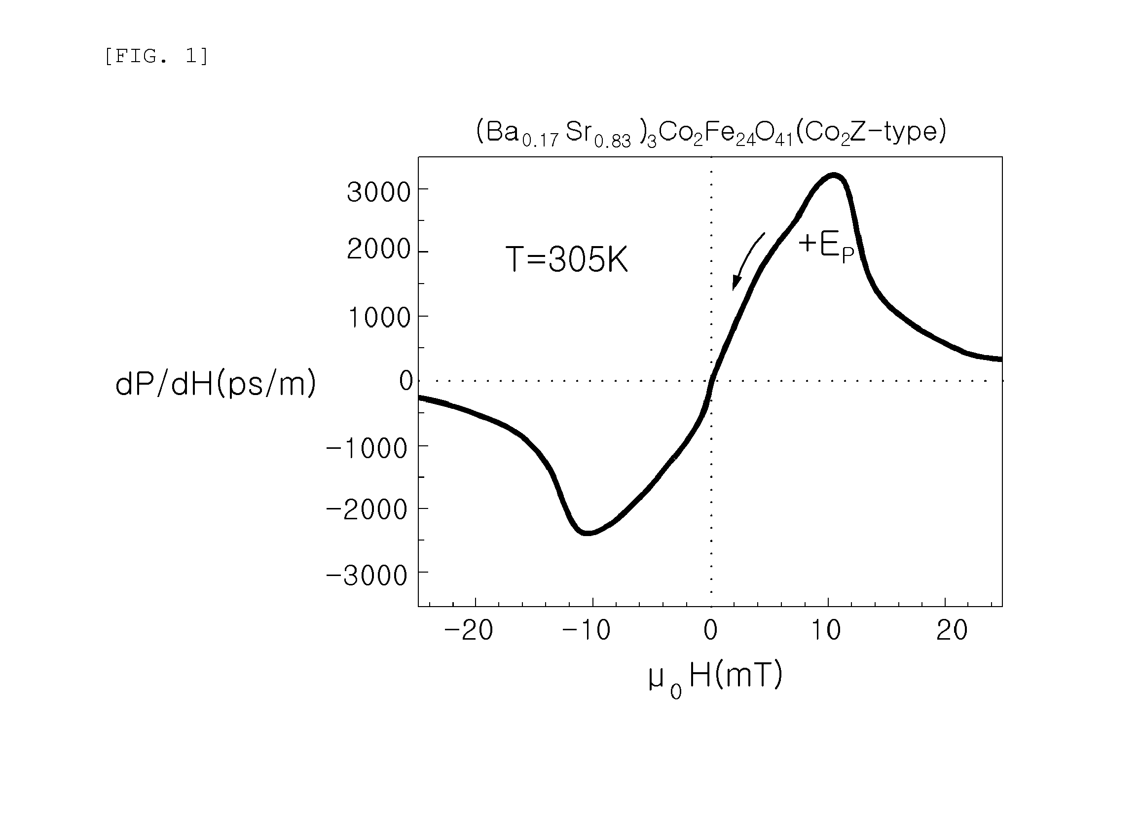
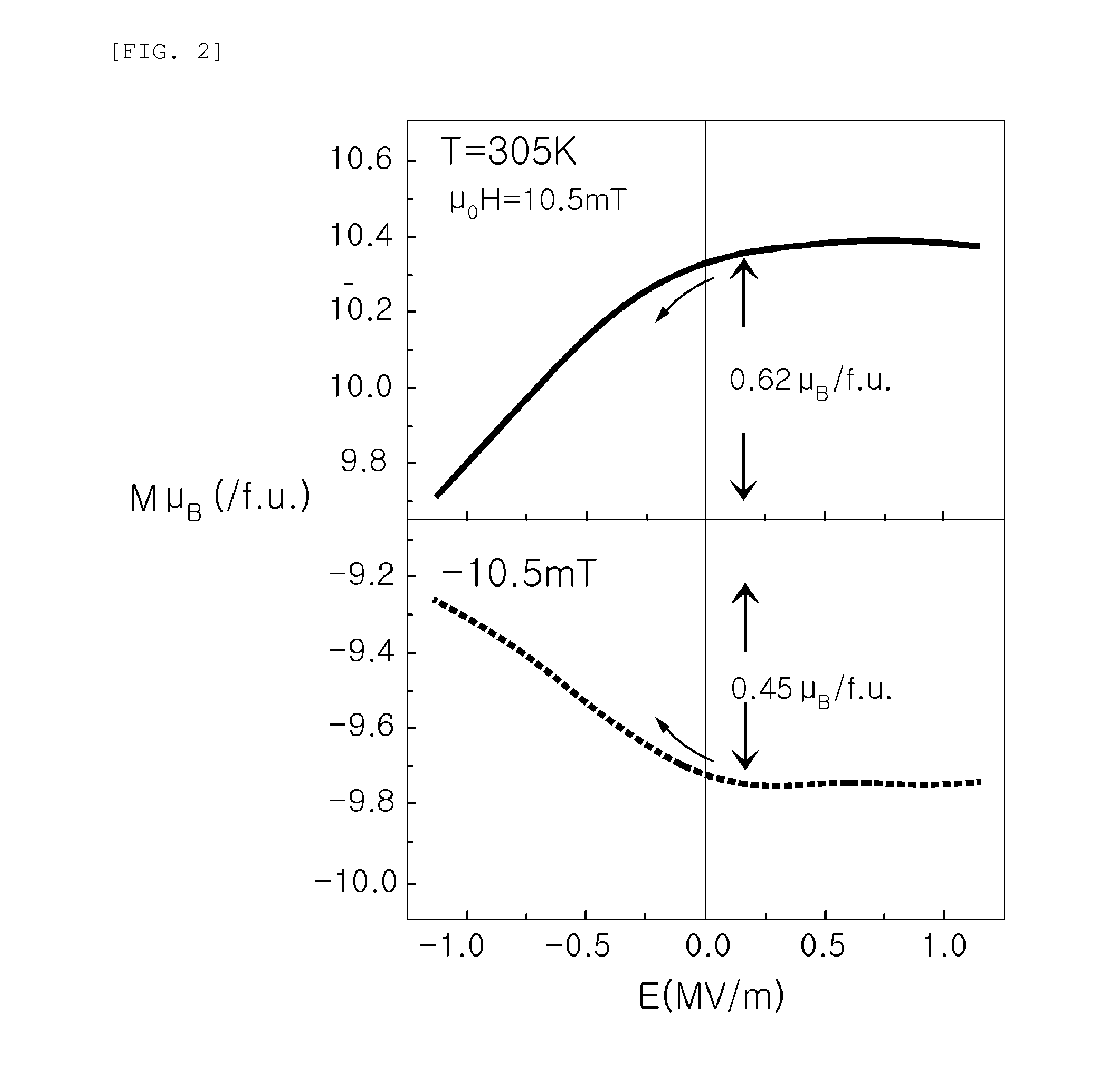
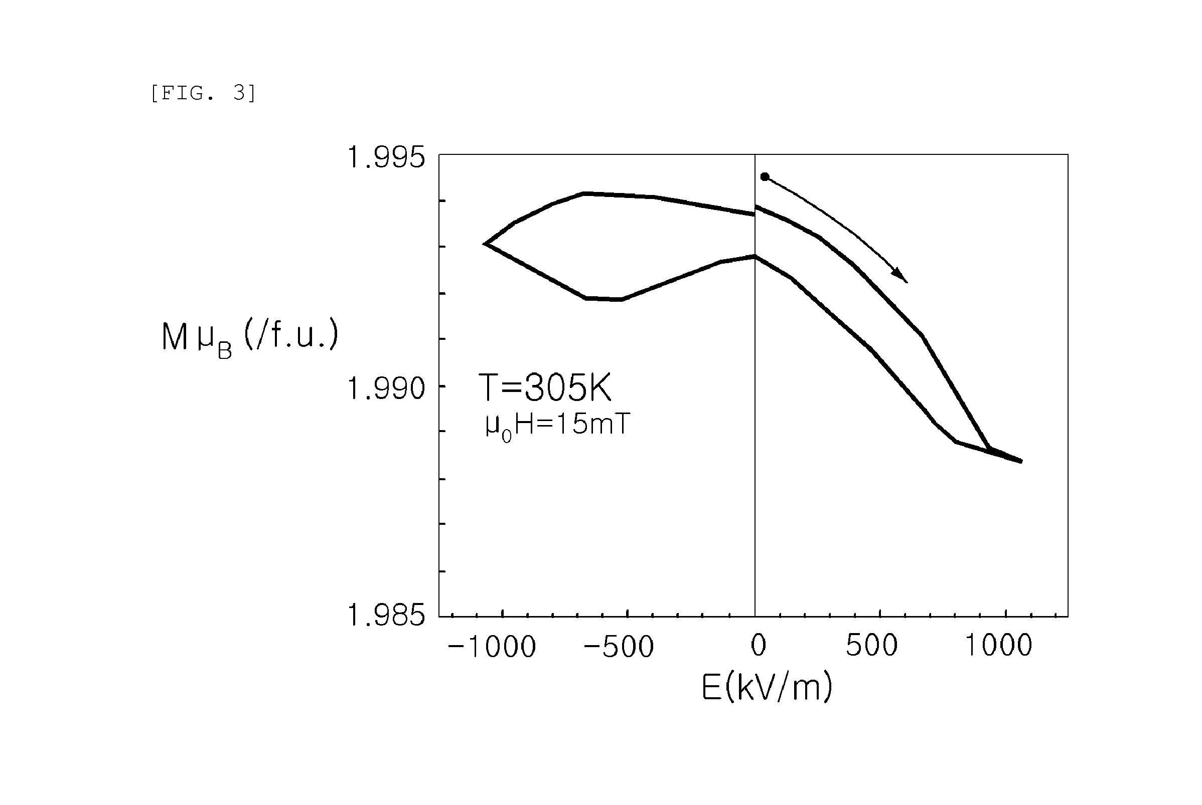
- A magnetoelectric material is developed by controlling the distance between magnetic ions using non-magnetic ions or alkaline earth metal ions, specifically through the inclusion of ions like aluminum or gallium and alkaline earth metal ions such as barium and strontium, which allows for magnetic property control by an electric field at normal temperatures, utilizing hexaferrite structures like Z-type and Y-type hexaferrites.

Material Safety and Environmental Regulations
The development and deployment of enhanced magnetoelectric materials for substrate interactions must comply with comprehensive safety protocols and environmental regulations across multiple jurisdictions. These materials often contain rare earth elements, transition metals, and engineered nanostructures that require careful handling throughout their lifecycle. Regulatory frameworks such as REACH (Registration, Evaluation, Authorization and Restriction of Chemicals) in Europe, TSCA (Toxic Substances Control Act) in the United States, and similar regulations in Asia-Pacific regions establish mandatory requirements for material characterization, toxicity assessment, and environmental impact evaluation.
Material safety considerations encompass both occupational health during manufacturing and end-user exposure risks. Magnetoelectric composites frequently incorporate ferrite particles, piezoelectric ceramics containing lead compounds, and magnetic alloys that may pose inhalation or dermal contact hazards. Manufacturing facilities must implement appropriate ventilation systems, personal protective equipment protocols, and waste management procedures. Worker exposure limits for constituent materials must be monitored according to OSHA standards and international equivalents.
Environmental regulations address the entire product lifecycle, from raw material extraction to end-of-life disposal. The presence of critical materials like neodymium, cobalt, and lead in magnetoelectric systems triggers specific reporting requirements under conflict minerals legislation and hazardous substance directives. Manufacturers must establish supply chain traceability and demonstrate compliance with RoHS (Restriction of Hazardous Substances) directives, particularly for electronic applications.
Substrate compatibility introduces additional regulatory complexity, as different substrate materials may create unique chemical interactions or degradation pathways. Silicon-based substrates generally present fewer regulatory challenges, while flexible polymer substrates may require evaluation under plastic additives regulations. The interface between magnetoelectric materials and substrates must be assessed for potential leaching, outgassing, or chemical migration that could impact safety classifications.
Emerging regulations specifically targeting nanomaterials and advanced functional materials are reshaping compliance requirements. The EU's Novel Materials Regulation and similar frameworks in other regions require extensive characterization of engineered nanoscale components commonly found in modern magnetoelectric systems. These regulations mandate detailed documentation of particle size distributions, surface modifications, and potential environmental transformation pathways.
Waste management and recycling protocols represent critical regulatory considerations, particularly given the strategic importance and environmental impact of rare earth elements. Extended Producer Responsibility frameworks increasingly require manufacturers to establish take-back programs and demonstrate sustainable end-of-life management strategies for magnetoelectric devices and their substrates.
Manufacturing Scalability for Enhanced Interfaces
Manufacturing scalability represents a critical bottleneck in translating enhanced magnetoelectric substrate interfaces from laboratory demonstrations to commercial applications. Current production methods for high-quality magnetoelectric composites rely heavily on sophisticated deposition techniques such as molecular beam epitaxy and pulsed laser deposition, which inherently limit throughput and increase per-unit costs. These precision-controlled processes, while essential for achieving optimal interface quality, present significant challenges when scaling to industrial production volumes.
The transition from small-scale research samples to large-area substrates introduces fundamental manufacturing complexities. Maintaining uniform interface properties across extended surfaces requires precise control of deposition parameters, substrate temperature distribution, and atmospheric conditions throughout the manufacturing process. Variations in these parameters can lead to inconsistent magnetoelectric coupling coefficients and reduced device performance, making quality control increasingly challenging as production scales expand.
Roll-to-roll processing emerges as a promising pathway for achieving manufacturing scalability, particularly for flexible magnetoelectric devices. This approach enables continuous production of magnetoelectric films on polymer substrates, potentially reducing manufacturing costs by orders of magnitude compared to batch processing methods. However, adapting high-temperature interface enhancement techniques to roll-to-roll compatible processes remains a significant technical challenge requiring innovative low-temperature synthesis approaches.
Cost-effective substrate preparation techniques represent another crucial scalability factor. Traditional substrate cleaning and surface modification processes often involve expensive vacuum systems and hazardous chemicals, limiting their applicability to high-volume manufacturing. Alternative approaches, including plasma-based surface treatments and solution-processed interface layers, offer potential pathways to reduce manufacturing complexity while maintaining interface quality standards.
Standardization of manufacturing protocols becomes increasingly important as production scales increase. Establishing reproducible process parameters, quality metrics, and testing procedures ensures consistent product performance across different manufacturing facilities and production runs. This standardization effort requires close collaboration between research institutions and industrial partners to translate laboratory-optimized processes into robust manufacturing procedures suitable for commercial implementation.
Unlock deeper insights with PatSnap Eureka Quick Research — get a full tech report to explore trends and direct your research. Try now!
Generate Your Research Report Instantly with AI Agent
Supercharge your innovation with PatSnap Eureka AI Agent Platform!