

Enhancing Circuit Density in Substrate-Like PCBs for EVs
APR 22, 20269 MIN READ
Generate Your Research Report Instantly with AI Agent
Patsnap Eureka helps you evaluate technical feasibility & market potential.
EV PCB Circuit Density Enhancement Background and Objectives
The automotive industry is undergoing a transformative shift toward electrification, driven by stringent environmental regulations, consumer demand for sustainable transportation, and technological advancements in battery systems. Electric vehicles represent a paradigm change from traditional internal combustion engines, requiring sophisticated electronic control systems to manage power distribution, battery management, motor control, and advanced driver assistance systems. This transition has created unprecedented demands on electronic packaging technologies, particularly printed circuit boards that serve as the backbone of EV electronic systems.
Traditional PCB technologies, originally developed for consumer electronics and telecommunications applications, face significant limitations when applied to automotive environments. Electric vehicles operate under extreme conditions including wide temperature ranges, high vibration levels, electromagnetic interference, and stringent reliability requirements over extended operational lifespans. The complexity of EV systems necessitates integration of multiple high-power electronic modules within increasingly constrained physical spaces, creating critical challenges for circuit density optimization.
The evolution toward substrate-like PCB architectures represents a convergence of semiconductor packaging technologies with traditional PCB manufacturing processes. These advanced substrates incorporate fine-pitch interconnects, embedded components, and multi-layer routing capabilities that enable higher circuit densities while maintaining the mechanical robustness required for automotive applications. The substrate-like approach bridges the gap between rigid PCBs and semiconductor substrates, offering enhanced electrical performance and miniaturization potential.
Current market pressures demand continuous reduction in electronic module sizes while simultaneously increasing functionality and power handling capabilities. Automotive manufacturers seek to optimize vehicle weight, improve aerodynamics, and maximize interior space utilization, all of which require more compact electronic packaging solutions. The challenge extends beyond simple miniaturization to encompass thermal management, signal integrity, and manufacturing cost optimization within high-volume production constraints.
The primary objective of enhancing circuit density in substrate-like PCBs for EVs encompasses developing manufacturing processes, materials, and design methodologies that enable significant increases in interconnect density while maintaining automotive-grade reliability standards. This involves advancing via formation technologies, implementing finer trace geometries, optimizing layer stackup configurations, and integrating passive components directly within substrate structures. Success in this domain will enable next-generation EV architectures with improved performance, reduced system complexity, and enhanced cost-effectiveness across the automotive supply chain.
Market Demand for High-Density EV Electronic Systems
The electric vehicle industry is experiencing unprecedented growth, driving substantial demand for advanced electronic systems that require increasingly sophisticated circuit density solutions. Modern EVs integrate multiple complex subsystems including battery management systems, power electronics, autonomous driving sensors, infotainment platforms, and thermal management controls, all of which demand compact yet powerful electronic architectures.
Battery management systems represent one of the most critical applications requiring high-density PCB solutions. These systems must monitor hundreds of individual cells while managing power distribution, thermal regulation, and safety protocols within severely constrained spaces. The integration of multiple voltage domains and high-current switching circuits necessitates substrate-like PCB technologies that can accommodate dense component placement while maintaining electrical isolation and thermal performance.
Power electronics modules in EVs are transitioning toward higher switching frequencies and increased power densities to improve efficiency and reduce system weight. Silicon carbide and gallium nitride semiconductors enable these performance improvements but require PCB substrates with enhanced thermal conductivity and reduced parasitic inductance. The market demands solutions that can support component densities exceeding traditional automotive electronics by significant margins.
Autonomous driving systems create additional complexity through their requirement for multiple high-speed processors, sensor interfaces, and communication modules. These systems process vast amounts of data from cameras, lidar, radar, and ultrasonic sensors, requiring PCB architectures that can support high-frequency signals while minimizing electromagnetic interference. The integration of artificial intelligence processing units further intensifies the demand for advanced substrate technologies.
The charging infrastructure evolution toward ultra-fast charging capabilities introduces new requirements for high-voltage, high-current electronics that must operate reliably in harsh automotive environments. Onboard chargers and DC-DC converters require PCB solutions that can handle increased power densities while maintaining safety standards and electromagnetic compatibility.
Market pressures for cost reduction and miniaturization continue to intensify as EV manufacturers seek to achieve price parity with internal combustion vehicles. This economic driver creates strong demand for PCB technologies that can integrate multiple functions onto single substrates while reducing overall system complexity and manufacturing costs.
The transition toward centralized vehicle architectures, where fewer but more powerful electronic control units replace distributed systems, further amplifies the need for high-density PCB solutions capable of supporting diverse functional requirements within consolidated hardware platforms.
Current State and Challenges of Substrate-Like PCB Density
The current landscape of substrate-like PCB technology for electric vehicles presents a complex interplay of advancing capabilities and persistent technical barriers. Modern substrate-like PCBs have achieved significant miniaturization through advanced manufacturing processes, with line widths reaching 25-30 micrometers and via diameters as small as 50-75 micrometers. These achievements represent substantial progress from traditional PCB technologies, enabling higher component integration densities essential for EV power management systems.
Contemporary manufacturing techniques employ modified IC fabrication processes, including photolithography and chemical etching methods adapted from semiconductor industry practices. Leading manufacturers have successfully implemented multi-layer structures with up to 8-12 conductive layers, utilizing thin dielectric materials with thicknesses ranging from 15-25 micrometers. This technological foundation supports the integration of high-density interconnects required for advanced EV control units and power conversion systems.
Despite these advancements, several critical challenges continue to constrain further density improvements. Thermal management remains a primary concern, as increased circuit density generates concentrated heat loads that exceed current dissipation capabilities. The coefficient of thermal expansion mismatch between different materials creates reliability issues under the extreme temperature cycling conditions typical in automotive environments, ranging from -40°C to 150°C operational requirements.
Manufacturing yield rates present another significant obstacle, with defect densities increasing exponentially as feature sizes approach current technological limits. The precision required for fine-pitch interconnects demands extremely controlled manufacturing environments, resulting in higher production costs and longer lead times. Quality control becomes increasingly complex as inspection technologies struggle to detect micro-defects that can cause field failures.
Material limitations further compound these challenges, particularly in dielectric layer performance and copper conductor reliability at reduced dimensions. Current polymer-based dielectrics exhibit insufficient dimensional stability for next-generation density requirements, while copper migration and electromigration phenomena become more pronounced at smaller geometries. The automotive qualification standards, including AEC-Q100 compliance, impose additional constraints on material selection and process optimization.
Signal integrity degradation emerges as circuit densities increase, with crosstalk, electromagnetic interference, and power delivery network performance becoming critical limiting factors. The proximity of high-speed digital signals to power electronics creates unique challenges not encountered in traditional consumer electronics applications, requiring innovative design approaches and advanced simulation capabilities to ensure reliable operation in EV environments.
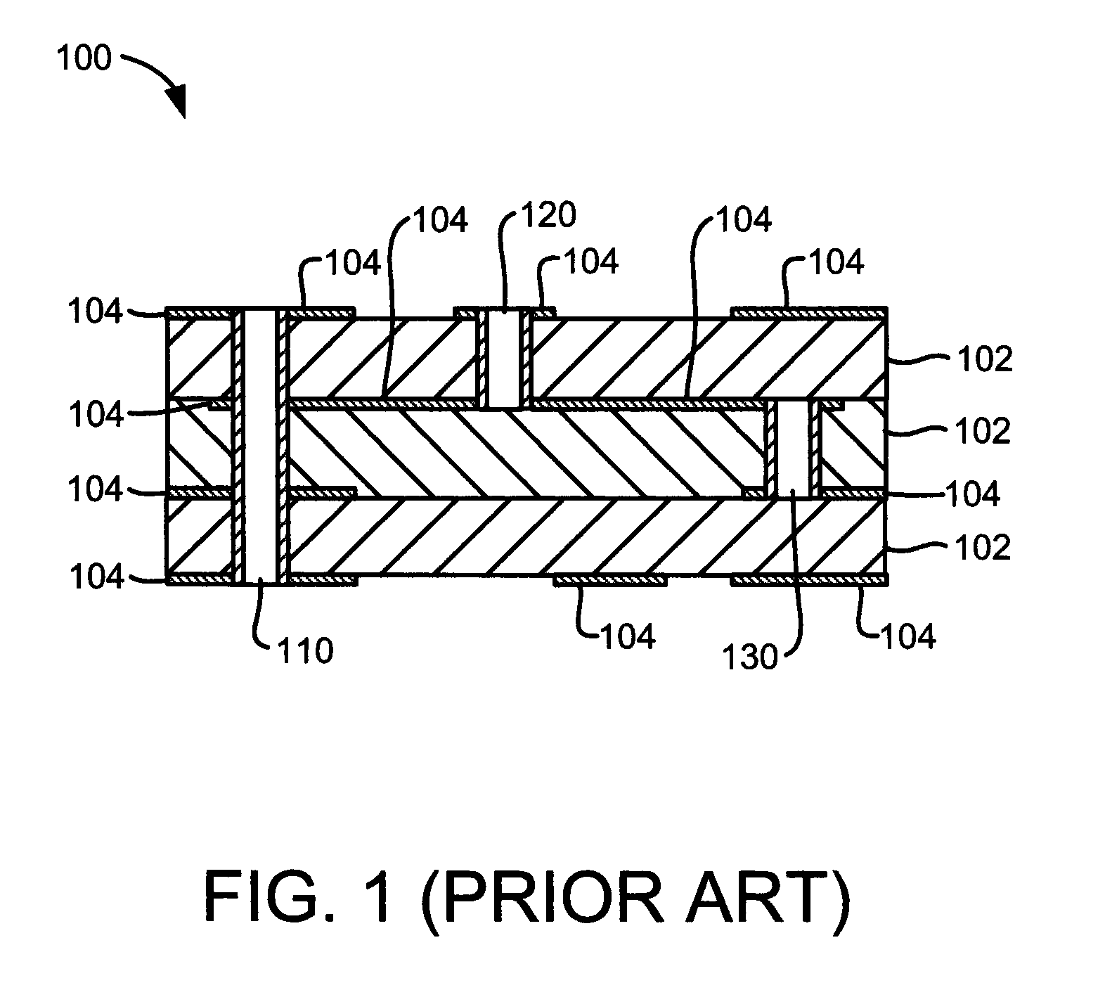
Existing Solutions for Maximizing Circuit Density in PCBs
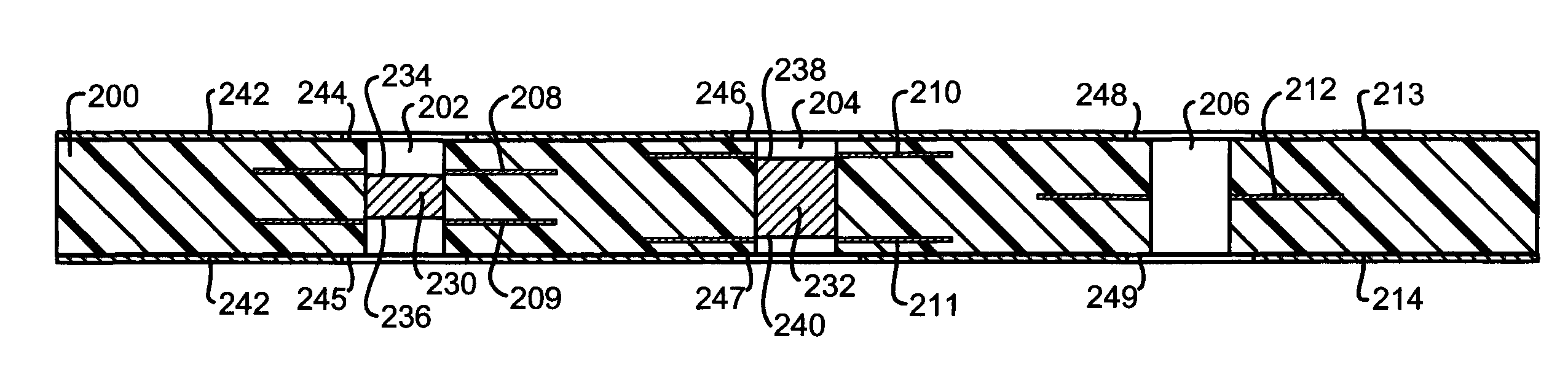
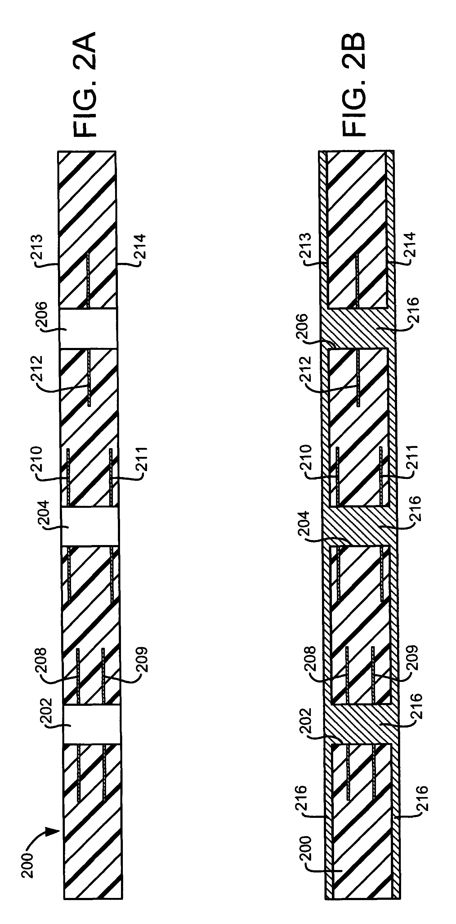
01 High-density interconnect (HDI) PCB structures
Substrate-like PCBs utilize high-density interconnect technology to achieve increased circuit density. This involves the use of microvias, fine line traces, and advanced layer stacking techniques to create compact circuit layouts. HDI structures enable more routing channels in smaller areas, allowing for miniaturization of electronic devices while maintaining or improving electrical performance. The technology incorporates laser-drilled vias and sequential build-up processes to achieve higher wiring density compared to traditional PCB manufacturing methods.- High-density interconnect (HDI) PCB structures: Substrate-like PCBs utilize high-density interconnect technology to achieve increased circuit density. This involves using microvias, fine-line traces, and multiple layer stackups to accommodate more circuits in a smaller area. HDI technology enables the creation of complex routing patterns with reduced trace widths and spacing, allowing for higher component density and improved electrical performance. The use of laser-drilled microvias and sequential lamination processes are key techniques in achieving these high-density configurations.
- Embedded component technology for space optimization: Embedding passive and active components within the PCB substrate layers is an effective method to increase circuit density. This technology involves integrating resistors, capacitors, and even semiconductor dies into the inner layers of the board, freeing up surface area for additional components and routing. The embedded approach reduces the overall board thickness while maintaining or improving functionality, and helps minimize signal path lengths for better electrical performance. This technique is particularly valuable in applications requiring compact form factors.
- Advanced layer stackup configurations: Optimizing the layer stackup design is crucial for achieving higher circuit density in substrate-like PCBs. This involves strategic arrangement of signal, power, and ground layers to maximize routing efficiency while maintaining signal integrity. Multi-layer designs with thin dielectric materials enable more layers to be incorporated within a given thickness constraint. The use of specialized core and prepreg materials with controlled dielectric properties allows for tighter layer spacing and improved impedance control, facilitating denser circuit layouts.
- Fine-pitch via and pad structures: Implementing fine-pitch via and pad structures is essential for increasing circuit density in substrate-like PCBs. This includes the use of smaller via diameters, reduced pad sizes, and tighter pitch spacing between connection points. Advanced drilling and plating technologies enable the creation of microvias with diameters as small as several mils, allowing for more routing channels in constrained spaces. The optimization of via-in-pad designs and stacked via configurations further enhances space utilization and enables higher component placement density.
- Surface treatment and metallization techniques: Advanced surface treatment and metallization processes play a critical role in achieving high circuit density while maintaining reliability. These techniques include the application of thin copper layers with precise thickness control, specialized surface finishes that enable fine-pitch bonding, and selective metallization patterns that optimize conductor spacing. The use of semi-additive or modified semi-additive processes allows for the creation of finer trace geometries with better dimensional control compared to traditional subtractive methods, supporting the requirements of high-density circuit designs.
02 Embedded component technology for space optimization
Embedding passive and active components within the PCB substrate layers significantly increases circuit density by eliminating surface-mounted components. This approach reduces the overall board thickness and footprint while improving electrical performance through shorter interconnection paths. The embedded components are integrated into the dielectric layers during the manufacturing process, allowing for more efficient use of board space and enabling higher component density on remaining surface areas.Expand Specific Solutions03 Advanced via technology and stacking methods
Implementing advanced via structures such as stacked vias, staggered vias, and via-in-pad technology enhances circuit density in substrate-like PCBs. These techniques optimize vertical interconnections between layers, reducing the horizontal space required for routing. The use of filled and plated vias, along with optimized via placement strategies, allows for more efficient layer utilization and enables tighter component placement, thereby increasing overall circuit density.Expand Specific Solutions04 Fine pitch trace and spacing design
Achieving higher circuit density through reduced trace widths and spacing between conductors is a key characteristic of substrate-like PCBs. Advanced manufacturing processes enable the creation of fine pitch patterns with precise dimensional control. This includes the use of specialized etching techniques, high-resolution imaging, and controlled impedance designs that maintain signal integrity while maximizing routing density. The implementation of differential pair routing and controlled spacing parameters further optimizes the available board area.Expand Specific Solutions05 Multi-layer substrate construction and material selection
Substrate-like PCBs employ multi-layer construction with optimized material selection to achieve high circuit density. This involves the use of thin core materials, low-loss dielectrics, and advanced resin systems that support fine feature fabrication. The layer stack-up design incorporates multiple signal, power, and ground planes arranged to maximize routing efficiency while maintaining electrical performance. Material properties such as dielectric constant, thermal conductivity, and dimensional stability are carefully selected to support high-density circuit requirements.Expand Specific Solutions
Key Players in EV PCB and Substrate Manufacturing Industry
The substrate-like PCB technology for electric vehicles is experiencing rapid growth driven by the expanding EV market and increasing demands for higher circuit density and miniaturization. The competitive landscape spans multiple industry segments, with established automotive manufacturers like Nissan Motor, BYD, and Renault leading EV integration, while battery technology leaders including Contemporary Amperex Technology (CATL), SK On, and CALB Group drive power system innovations. Technology giants such as Samsung Electronics, Intel, and Samsung Electro-Mechanics contribute advanced semiconductor and component solutions. The technology maturity varies significantly across players, with semiconductor companies like SK Hynix and materials specialists like 3M Innovative Properties demonstrating high technical sophistication, while emerging companies and research institutions including Industrial Technology Research Institute and various universities are advancing next-generation solutions, indicating a dynamic ecosystem transitioning from early adoption to mainstream implementation.
Intel Corp.
Technical Solution: Intel has developed embedded multi-die interconnect bridge (EMIB) technology and advanced packaging solutions that enhance circuit density for automotive applications. Their approach combines substrate-like PCB technology with advanced interconnect solutions, utilizing fine-pitch routing and high-density via structures. Intel's technology employs organic substrates with enhanced thermal management capabilities and incorporates advanced materials for improved signal integrity. The company's packaging solutions feature ultra-high-density interconnects with pitch scaling down to sub-40μm levels. Their automotive-grade solutions include specialized design rules for power delivery networks and thermal dissipation optimized for EV power electronics and control systems requiring compact form factors and high reliability.
Strengths: Advanced packaging expertise and strong thermal management solutions. Weaknesses: Limited focus on automotive-specific applications and higher complexity in manufacturing processes.
Samsung Electro-Mechanics Co., Ltd.
Technical Solution: Samsung Electro-Mechanics has developed advanced substrate-like PCB (SLP) technology specifically for high-density circuit applications in electric vehicles. Their approach utilizes ultra-fine line/space patterns down to 15/15μm and employs modified semi-additive processes (mSAP) to achieve superior circuit density. The company implements multi-layer build-up structures with thin dielectric materials and optimized via formation techniques. Their SLP technology incorporates advanced materials including low-loss dielectrics and high-performance copper foils designed for automotive temperature ranges. The manufacturing process includes precision laser drilling for microvias and specialized plating processes to ensure reliable interconnections in demanding EV environments.
Strengths: Industry-leading fine line capabilities and proven automotive qualification processes. Weaknesses: Higher manufacturing costs compared to traditional PCB technologies and complex process control requirements.
Core Innovations in Substrate-Like PCB Design Techniques
Method of forming a substrate having a plurality of insulator layers
PatentInactiveUS8136240B2
Innovation
- The implementation of photolithographic techniques to create plated-through-hole (PTH) plugs of controlled, variable depth in through-holes, allowing for the horizontal splitting of conductive vias, thereby increasing wiring density without the need for additional fabrication steps.

Build-up printed circuit board structure for increasing fine circuit density and method of manufacturing the same
PatentInactiveUS20100044083A1
Innovation
- A method involving a core carrier board with multiple dielectric layers and two-step conductive blind holes, where each step forms conductive pads and circuits, increasing bump pitches and allowing for larger pad sizes and increased circuit density through a build-up process, including electroless copper, lithography, and electroplating processes.


Automotive Safety Standards for High-Density Electronic Systems
The automotive industry's transition toward electrification has necessitated the development of comprehensive safety standards specifically addressing high-density electronic systems in electric vehicles. These standards encompass critical aspects of circuit density enhancement while maintaining operational safety and reliability under extreme automotive conditions.
ISO 26262 serves as the foundational functional safety standard for automotive electrical and electronic systems, establishing safety integrity levels that directly impact high-density PCB design requirements. The standard mandates rigorous hazard analysis and risk assessment procedures for densely packed electronic components, requiring manufacturers to implement systematic approaches to failure mode identification and mitigation strategies.
IPC-2221 and IPC-2222 standards provide specific guidelines for automotive PCB design, addressing spacing requirements, thermal management, and electrical isolation in high-density configurations. These standards establish minimum clearance distances between conductors and components, which become increasingly challenging to maintain as circuit density increases in substrate-like PCB architectures.
The Automotive Electronics Council's AEC-Q100 qualification standard defines stress testing requirements for integrated circuits used in automotive applications. For high-density systems, this standard becomes particularly relevant as thermal cycling, humidity exposure, and mechanical stress testing must account for the increased heat generation and reduced thermal dissipation pathways inherent in densely packed designs.
EMC compliance requirements under CISPR 25 and ISO 11452 present unique challenges for high-density automotive electronics. The proximity of high-speed digital circuits, power management systems, and sensitive analog components in compact PCB layouts requires sophisticated shielding strategies and careful signal routing to prevent electromagnetic interference that could compromise vehicle safety systems.
Recent developments in automotive cybersecurity standards, including ISO/SAE 21434, introduce additional considerations for high-density electronic systems. The standard requires secure hardware design practices that must be balanced against density optimization goals, ensuring that security features do not compromise the physical constraints of substrate-like PCB implementations while maintaining robust protection against cyber threats in connected vehicle architectures.
Thermal Management Solutions for Dense EV Circuit Boards
As electric vehicle circuit boards achieve unprecedented component density, thermal management becomes the critical bottleneck determining system reliability and performance. Dense substrate-like PCBs generate concentrated heat loads that can exceed 50W/cm² in power electronics sections, creating thermal hotspots that threaten component integrity and system longevity. Traditional air-cooling approaches prove inadequate for these high-density configurations, necessitating advanced thermal solutions specifically engineered for automotive environments.
Liquid cooling systems represent the most promising approach for dense EV circuit boards, utilizing direct contact cooling plates or embedded microchannels within the substrate structure. These solutions can achieve thermal resistance values below 0.1°C/W while maintaining compact form factors essential for automotive applications. Advanced implementations incorporate phase-change materials and vapor chamber technologies to enhance heat spreading across the board surface, effectively mitigating localized thermal stress concentrations.
Thermal interface materials play a crucial role in dense PCB thermal management, with next-generation solutions featuring thermal conductivities exceeding 10W/mK. Graphene-enhanced thermal pads and liquid metal interfaces provide superior heat transfer pathways between high-power components and cooling systems. These materials must withstand automotive temperature cycling requirements while maintaining consistent thermal performance over extended operational periods.
Innovative substrate materials incorporating thermally conductive fillers offer integrated thermal management capabilities. Ceramic-filled polymer substrates and metal-core PCB technologies provide enhanced heat dissipation directly through the board structure, reducing reliance on external cooling systems. These solutions enable thermal conductivity improvements of 300-500% compared to standard FR4 materials while preserving electrical performance characteristics.
Advanced thermal simulation and real-time monitoring systems enable predictive thermal management for dense EV circuits. Machine learning algorithms optimize cooling system operation based on driving patterns and component loading, maximizing thermal efficiency while minimizing energy consumption. Integrated temperature sensors and thermal imaging capabilities provide continuous monitoring of critical thermal zones, enabling proactive thermal management strategies that prevent performance degradation and extend component lifespan in high-density automotive electronic systems.
Unlock deeper insights with Patsnap Eureka Quick Research — get a full tech report to explore trends and direct your research. Try now!
Generate Your Research Report Instantly with AI Agent
Supercharge your innovation with Patsnap Eureka AI Agent Platform!