

Evaluate Particle Adhesion Prevention Techniques for Reticle Pellicles
MAY 21, 20269 MIN READ
Generate Your Research Report Instantly with AI Agent
PatSnap Eureka helps you evaluate technical feasibility & market potential.
Pellicle Particle Contamination Background and Objectives
Reticle pellicles represent a critical component in advanced semiconductor lithography systems, serving as protective membranes that shield photomasks from airborne contaminants during the exposure process. These ultra-thin polymer films, typically measuring 100-200 nanometers in thickness, are mounted several millimeters above the reticle surface to create a protective barrier while maintaining optical transparency for precise pattern transfer.
The semiconductor industry's relentless pursuit of smaller feature sizes has intensified the challenges associated with pellicle contamination. As lithography wavelengths have progressed from 365nm to 248nm, 193nm, and now extreme ultraviolet (EUV) at 13.5nm, the tolerance for particle contamination has decreased exponentially. Even sub-10nm particles can cause critical defects that result in yield loss and device failure.
Particle adhesion on pellicle surfaces occurs through various mechanisms including van der Waals forces, electrostatic attraction, and capillary forces from moisture. These contaminants originate from multiple sources within the lithography environment, including outgassing from photoresist materials, mechanical wear from wafer handling systems, and residual particles from cleanroom air filtration systems.
The evolution toward EUV lithography has introduced unprecedented challenges for pellicle technology. Traditional pellicle materials face degradation under high-energy EUV radiation, while the requirement for hydrogen environments in EUV scanners creates additional contamination pathways. Current pellicle solutions struggle to maintain both optical performance and contamination resistance under these extreme conditions.
Primary objectives for particle adhesion prevention techniques encompass developing surface treatments that minimize particle attraction forces while preserving optical transmission properties. Advanced coating technologies, electrostatic mitigation strategies, and novel pellicle materials represent key research directions. Additionally, real-time monitoring systems for early contamination detection and automated cleaning protocols are essential for maintaining production efficiency.
The technical goals extend beyond simple contamination prevention to include extending pellicle lifetime, reducing replacement frequency, and minimizing production downtime. Success in these areas directly impacts semiconductor manufacturing economics, where each hour of scanner downtime can cost hundreds of thousands of dollars in lost production capacity.
Market Demand for Advanced Pellicle Protection Solutions
The semiconductor manufacturing industry faces unprecedented challenges in maintaining yield rates as device geometries continue to shrink below 7nm nodes. Advanced lithography processes demand exceptional cleanliness standards, driving substantial market demand for sophisticated pellicle protection solutions that can effectively prevent particle contamination on photomasks during exposure operations.
Market drivers stem primarily from the exponential cost increase of photomask replacement and production delays caused by particle-induced defects. Leading foundries report that a single contaminated reticle can result in production losses exceeding hundreds of thousands of dollars per incident, creating urgent demand for reliable particle adhesion prevention technologies. The transition to extreme ultraviolet lithography has further intensified these requirements, as traditional pellicle materials face thermal and chemical stability challenges under EUV radiation.
The automotive semiconductor sector represents a rapidly expanding market segment, where reliability requirements for advanced driver assistance systems and autonomous vehicle components necessitate zero-defect manufacturing standards. This sector's growth trajectory significantly amplifies demand for advanced pellicle protection solutions, particularly those capable of maintaining performance across extended production runs without degradation.
Memory manufacturers constitute another major demand driver, as high-volume production of DRAM and NAND flash devices requires consistent yield optimization. The industry's shift toward 3D memory architectures with increasingly complex multi-layer structures has created new contamination vulnerability points, expanding the addressable market for comprehensive pellicle protection systems.
Emerging applications in quantum computing and photonics manufacturing are generating additional market opportunities for specialized pellicle solutions. These applications often require custom contamination control approaches due to unique material sensitivities and processing environments, creating premium market segments for advanced protection technologies.
Regional demand patterns show concentrated growth in Asia-Pacific manufacturing hubs, where major foundries and memory manufacturers are expanding production capacity. This geographic concentration creates opportunities for localized solution development and support services, while also driving competitive pressure for cost-effective protection technologies that can scale with high-volume manufacturing requirements.
Current Particle Adhesion Issues and Technical Barriers
Particle adhesion on reticle pellicles represents one of the most critical challenges in advanced semiconductor lithography, directly impacting yield rates and manufacturing efficiency. Current pellicle materials, primarily consisting of organic polymers with thickness ranging from 100-300 nanometers, exhibit inherent susceptibility to particle attraction and retention due to electrostatic forces, van der Waals interactions, and surface energy characteristics.
The fundamental physics governing particle adhesion involves multiple force mechanisms operating simultaneously. Electrostatic attraction occurs when charged particles encounter pellicle surfaces that have accumulated static charge during handling or processing. Van der Waals forces become dominant for particles smaller than 50 nanometers, creating strong adhesion that conventional cleaning methods cannot overcome. Surface roughness at the nanoscale level creates mechanical interlocking sites where particles become physically trapped.
Manufacturing environments introduce additional complexity through airborne contamination sources. Despite cleanroom protocols maintaining Class 1 conditions, submicron particles from photoresist outgassing, equipment wear, and human activity continuously threaten pellicle cleanliness. The pellicle's position directly above the reticle creates a particle collection zone where gravitational settling combines with electrostatic attraction to concentrate contaminants.
Current cleaning methodologies face significant limitations when addressing adhered particles. Traditional gas purging techniques prove ineffective against strongly bonded contaminants, while liquid cleaning risks pellicle damage due to material sensitivity. Ultrasonic cleaning methods can cause pellicle membrane rupture or delamination from support frames. Chemical cleaning agents often interact unpredictably with pellicle polymers, leading to optical property degradation or structural weakening.
Temperature cycling during lithography processes exacerbates particle adhesion through thermal expansion mismatches between particles and pellicle materials. This creates stress concentrations that can either strengthen existing bonds or cause particle embedding into the pellicle surface. The resulting defects become permanent features that cannot be removed through conventional cleaning approaches.
Electrostatic discharge events during pellicle handling represent another critical barrier. These events can create localized charge concentrations that attract particles with extraordinary force, making subsequent removal extremely difficult. Current antistatic measures provide only temporary protection and often lose effectiveness in low-humidity manufacturing environments.
Existing Particle Prevention Methods for Reticle Pellicles
01 Pellicle frame design and structure optimization
Optimized pellicle frame designs that minimize particle generation and adhesion through improved structural configurations. These designs focus on reducing turbulence and creating smoother airflow patterns around the pellicle to prevent particle accumulation on critical surfaces.- Pellicle frame design and structure optimization: Optimized pellicle frame designs that minimize particle generation and adhesion through improved structural configurations. These designs focus on reducing turbulence and creating smoother airflow patterns around the pellicle to prevent particle accumulation on critical surfaces.
- Electrostatic charge control methods: Techniques for controlling electrostatic charges on pellicle surfaces to prevent particle attraction and adhesion. These methods involve charge neutralization systems and conductive materials that reduce the electrostatic forces responsible for particle attachment to pellicle membranes.
- Surface treatment and coating technologies: Specialized surface treatments and coatings applied to pellicle components to create particle-repelling properties. These treatments modify surface energy and create smooth, low-adhesion surfaces that prevent particles from sticking to critical pellicle areas.
- Air flow management and filtration systems: Advanced air flow control and filtration mechanisms designed to maintain clean environments around pellicles. These systems include directional air flow patterns and high-efficiency filtration to remove particles before they can reach pellicle surfaces.
- Particle detection and removal mechanisms: Integrated systems for detecting and actively removing particles from pellicle surfaces. These mechanisms include monitoring technologies that identify particle contamination and automated cleaning processes that maintain pellicle cleanliness during operation.
02 Electrostatic charge control methods
Techniques for controlling electrostatic charges on pellicle surfaces to prevent particle attraction and adhesion. These methods involve charge neutralization systems and conductive materials that eliminate static buildup which can attract contaminant particles to the pellicle membrane.Expand Specific Solutions03 Surface treatment and coating technologies
Specialized surface treatments and coatings applied to pellicle components to create particle-repelling properties. These treatments modify surface energy and create smooth, non-adhesive surfaces that prevent particles from sticking to the pellicle membrane and frame structures.Expand Specific Solutions04 Airflow management and contamination control
Systems and methods for managing airflow patterns around pellicles to minimize particle deposition. These approaches include directional air curtains, laminar flow optimization, and pressure differential control to keep particles away from sensitive pellicle surfaces during semiconductor processing.Expand Specific Solutions05 Cleaning and maintenance mechanisms
Integrated cleaning systems and maintenance protocols designed to remove particles from pellicle surfaces without damage. These mechanisms include gentle cleaning methods, automated particle removal systems, and preventive maintenance approaches that maintain pellicle cleanliness throughout the manufacturing process.Expand Specific Solutions
Key Players in Pellicle and Lithography Equipment Industry
The particle adhesion prevention techniques for reticle pellicles market represents a mature yet evolving segment within the semiconductor lithography ecosystem. The industry is in a consolidation phase, driven by increasing demands for advanced node manufacturing and stringent contamination control requirements. Market dynamics are shaped by established players like ASML Netherlands BV, Applied Materials, and Nikon Corp., who dominate lithography equipment, while material specialists including Shin-Etsu Chemical, AGC Inc., and Mitsui Chemicals provide critical pellicle substrates and coatings. Technology maturity varies significantly across the competitive landscape - foundry leaders such as Taiwan Semiconductor Manufacturing, Samsung Electronics, and Intel Corp. drive demanding specifications, while emerging players like Shanghai Huali Microelectronics and ChangXin Memory Technologies represent growing regional capabilities. The market exhibits high barriers to entry due to complex technical requirements and established supplier relationships.
Shin-Etsu Chemical Co., Ltd.
Technical Solution: Shin-Etsu Chemical specializes in developing advanced polymer materials and surface treatment chemicals for pellicle applications with enhanced particle repulsion properties. Their solutions include silicone-based anti-adhesion coatings and fluoropolymer treatments that create low-energy surfaces resistant to particle contamination. The company's technology portfolio encompasses both preventive coatings and reactive cleaning agents designed to maintain pellicle transparency while minimizing particle accumulation during semiconductor manufacturing processes.
Strengths: Strong materials chemistry expertise, established supplier relationships in semiconductor industry. Weaknesses: Limited equipment integration capabilities, dependency on customer implementation expertise.
Samsung Electronics Co., Ltd.
Technical Solution: Samsung utilizes atomic layer deposition (ALD) and molecular beam epitaxy techniques to create ultra-smooth pellicle surfaces with controlled surface chemistry for particle adhesion prevention. Their technology incorporates fluorinated polymer coatings and nanostructured surface textures that reduce particle adhesion forces by modifying van der Waals interactions. The company has developed proprietary cleaning methodologies using plasma-activated gases and precision temperature control systems to maintain pellicle performance in high-throughput manufacturing environments.
Strengths: Comprehensive semiconductor manufacturing capabilities, strong materials science expertise. Weaknesses: Technology integration complexity, high development costs for new process nodes.
Core Patents in Anti-Adhesion Pellicle Technologies
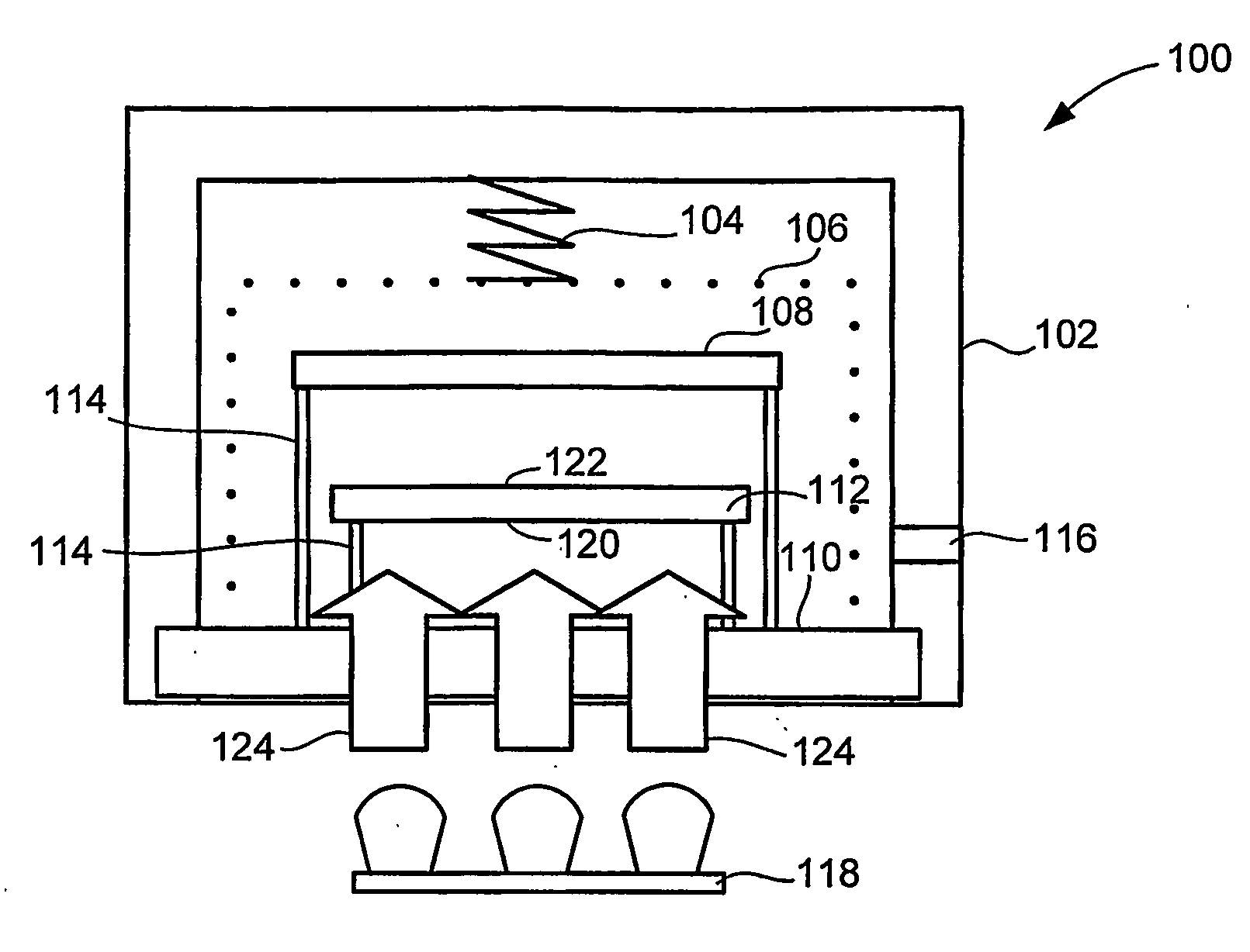
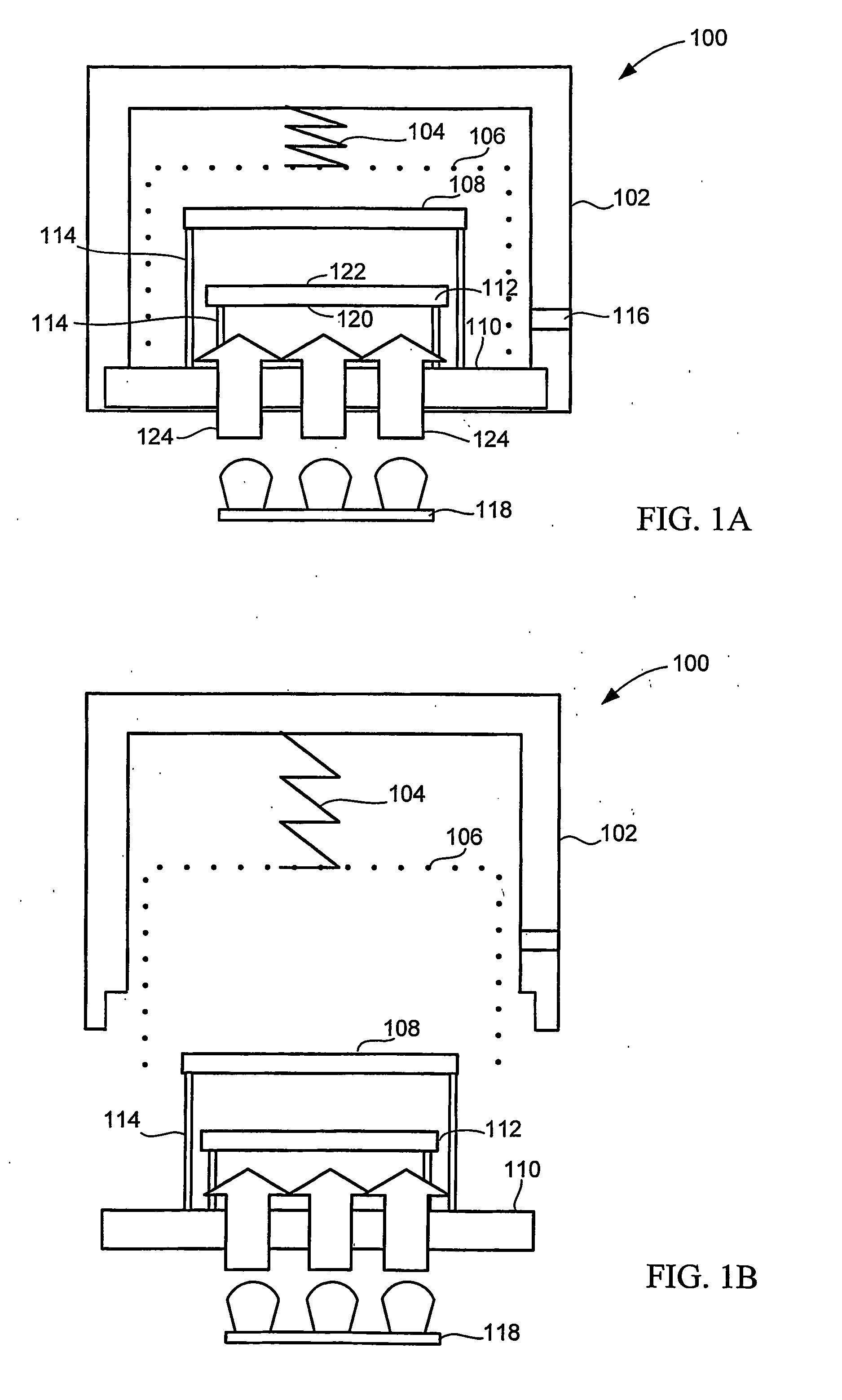
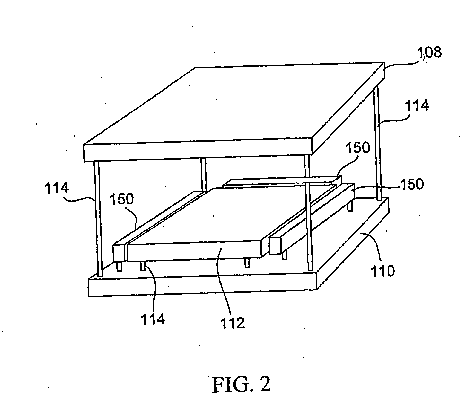
Thermophoretic Techniques for Protecting Reticles from Contaminants
PatentInactiveUS20070211232A1
Innovation
- The implementation of thermophoresis by maintaining the reticle at a higher temperature than its surroundings, using plates at a lower temperature positioned proximate to the reticle to create a temperature gradient that repels contaminants, effectively protecting the reticle from particles during storage, handling, and use within the lithography system.

Pellicle manufacturing method and method for manufacturing photomask with pellicle
PatentWO2016175019A1
Innovation
- A method involving the use of adhesive sheets with decreasing adhesive strength when subjected to external stimuli is applied to both sides of the substrate, allowing for precise cutting and separation of the pellicle frame while capturing foreign particles, thereby preventing their adhesion to the pellicle membrane. This method includes exposing the pellicle film from the opposite substrate surface, attaching adhesive sheets to cover the cutting area, and using stealth dicing or other techniques to minimize dust generation.


Cleanroom Standards and Contamination Control Regulations
The semiconductor manufacturing industry operates under stringent cleanroom standards that directly impact particle adhesion prevention strategies for reticle pellicles. ISO 14644 series standards define the fundamental framework for cleanroom classification, establishing particle concentration limits that range from ISO Class 1 (≤10 particles/m³ of ≥0.1 μm) to ISO Class 9. For advanced lithography processes, particularly those involving EUV and deep UV technologies, ISO Class 1 or 2 cleanrooms are mandatory to minimize particle contamination risks on pellicle surfaces.
Federal Standard 209E, though superseded by ISO standards in many regions, continues to influence cleanroom design principles and contamination control protocols. The standard's emphasis on airflow patterns, filtration efficiency, and personnel protocols remains relevant for pellicle handling environments. Modern facilities typically implement unidirectional airflow systems with HEPA or ULPA filtration achieving 99.9995% efficiency for particles ≥0.12 μm, creating laminar flow conditions that prevent particle settlement on critical surfaces.
SEMI standards, particularly SEMI F20 for specification and guidelines for particle monitoring systems, establish protocols for real-time contamination detection in pellicle manufacturing and storage areas. These standards mandate continuous monitoring of airborne molecular contamination (AMC) and particle levels, with alert thresholds typically set at 50% of the maximum allowable contamination levels. The integration of laser particle counters and condensation particle counters enables immediate detection of contamination events that could compromise pellicle integrity.
Regulatory compliance extends beyond particle concentration limits to encompass material compatibility requirements. SEMI F21 guidelines address outgassing specifications for cleanroom materials, ensuring that construction materials, equipment, and consumables do not contribute to molecular contamination that could enhance particle adhesion through chemical interactions. These regulations specify maximum allowable outgassing rates for acids, bases, condensables, and dopants, typically measured in ng/cm²/min.
International standards also address electrostatic discharge (ESD) control, which significantly impacts particle behavior near pellicle surfaces. IEC 61340 series standards establish requirements for ESD control programs, including ionization systems that neutralize static charges responsible for attracting particles to pellicle surfaces. Proper implementation of these standards reduces electrostatic particle adhesion by maintaining surface potentials within ±50V ranges.
Environmental Impact of Pellicle Manufacturing Processes
The manufacturing of reticle pellicles involves several industrial processes that generate significant environmental impacts across multiple dimensions. Traditional pellicle fabrication relies heavily on fluoropolymer materials, particularly perfluorinated compounds, which pose substantial environmental concerns due to their persistence in ecosystems and potential bioaccumulation properties. The production of these materials requires energy-intensive polymerization processes that contribute to greenhouse gas emissions and consume considerable amounts of fossil fuel-derived energy.
Chemical waste generation represents a critical environmental challenge in pellicle manufacturing. The fabrication process involves extensive use of organic solvents, etching chemicals, and cleaning agents that require proper disposal and treatment. Many of these chemicals contain volatile organic compounds (VOCs) that can contribute to air pollution and ozone depletion. Additionally, the precision cleaning processes necessary for pellicle quality generate contaminated wastewater streams containing fluorinated compounds that are difficult to remediate using conventional treatment methods.
The membrane stretching and mounting processes consume significant amounts of water for cleaning and quality control procedures. This water usage, combined with the need for ultrapure water systems, places additional strain on local water resources. The energy requirements for maintaining cleanroom environments, temperature control, and specialized equipment operation contribute substantially to the carbon footprint of pellicle manufacturing facilities.
Packaging and transportation of pellicles also present environmental considerations, as these delicate components require specialized protective packaging materials and controlled shipping conditions. The global nature of semiconductor supply chains means that pellicles often travel long distances between manufacturing sites and end users, adding to transportation-related emissions.
Recent industry initiatives have focused on developing more sustainable manufacturing approaches, including solvent recovery systems, energy-efficient cleanroom designs, and alternative materials with reduced environmental impact. However, the stringent quality requirements for semiconductor applications limit the adoption of certain green manufacturing techniques, creating ongoing tension between environmental sustainability and product performance requirements.
Unlock deeper insights with PatSnap Eureka Quick Research — get a full tech report to explore trends and direct your research. Try now!
Generate Your Research Report Instantly with AI Agent
Supercharge your innovation with PatSnap Eureka AI Agent Platform!