

Evaluate Surface Mount Technology on Substrate-Like PCBs
APR 22, 20269 MIN READ
Generate Your Research Report Instantly with AI Agent
PatSnap Eureka helps you evaluate technical feasibility & market potential.
SMT on Substrate-Like PCB Technology Background and Goals
Surface Mount Technology (SMT) has undergone significant evolution since its introduction in the 1960s, transforming from a niche assembly method to the dominant approach in modern electronics manufacturing. The technology emerged as a response to the increasing demand for miniaturization, higher component density, and improved electrical performance in electronic devices. Initially developed for military and aerospace applications, SMT has expanded across all sectors of the electronics industry.
The evolution of SMT has been closely intertwined with advances in substrate technology. Traditional printed circuit boards (PCBs) served as the primary platform for SMT implementation for decades. However, the relentless push toward higher performance, increased functionality, and reduced form factors has driven the development of substrate-like PCBs that blur the lines between conventional PCBs and advanced semiconductor substrates.
Substrate-like PCBs represent a convergence of PCB manufacturing techniques with semiconductor packaging technologies. These advanced substrates incorporate features such as ultra-fine line widths, microvias, embedded components, and multi-layer stackups with controlled impedance characteristics. They enable the integration of passive components within the substrate structure and support advanced packaging concepts like system-in-package (SiP) and package-on-package (PoP) configurations.
The primary technical objectives driving SMT implementation on substrate-like PCBs include achieving higher interconnect density, reducing signal propagation delays, minimizing electromagnetic interference, and enabling three-dimensional packaging architectures. These goals align with industry demands for enhanced performance in applications such as 5G communications, artificial intelligence processors, automotive electronics, and Internet of Things devices.
Current technological targets focus on supporting component pitches below 0.3mm, implementing embedded passive integration, achieving layer-to-layer registration accuracy within ±10 micrometers, and maintaining signal integrity at frequencies exceeding 100 GHz. Additionally, thermal management objectives include developing substrate materials and structures that can effectively dissipate heat from high-power density components while maintaining dimensional stability during assembly processes.
The strategic importance of mastering SMT on substrate-like PCBs extends beyond immediate technical benefits, positioning organizations to capitalize on emerging market opportunities in next-generation electronics where traditional assembly approaches reach their physical and performance limitations.
The evolution of SMT has been closely intertwined with advances in substrate technology. Traditional printed circuit boards (PCBs) served as the primary platform for SMT implementation for decades. However, the relentless push toward higher performance, increased functionality, and reduced form factors has driven the development of substrate-like PCBs that blur the lines between conventional PCBs and advanced semiconductor substrates.
Substrate-like PCBs represent a convergence of PCB manufacturing techniques with semiconductor packaging technologies. These advanced substrates incorporate features such as ultra-fine line widths, microvias, embedded components, and multi-layer stackups with controlled impedance characteristics. They enable the integration of passive components within the substrate structure and support advanced packaging concepts like system-in-package (SiP) and package-on-package (PoP) configurations.
The primary technical objectives driving SMT implementation on substrate-like PCBs include achieving higher interconnect density, reducing signal propagation delays, minimizing electromagnetic interference, and enabling three-dimensional packaging architectures. These goals align with industry demands for enhanced performance in applications such as 5G communications, artificial intelligence processors, automotive electronics, and Internet of Things devices.
Current technological targets focus on supporting component pitches below 0.3mm, implementing embedded passive integration, achieving layer-to-layer registration accuracy within ±10 micrometers, and maintaining signal integrity at frequencies exceeding 100 GHz. Additionally, thermal management objectives include developing substrate materials and structures that can effectively dissipate heat from high-power density components while maintaining dimensional stability during assembly processes.
The strategic importance of mastering SMT on substrate-like PCBs extends beyond immediate technical benefits, positioning organizations to capitalize on emerging market opportunities in next-generation electronics where traditional assembly approaches reach their physical and performance limitations.
Market Demand Analysis for Advanced SMT Solutions
The global electronics manufacturing industry is experiencing unprecedented demand for advanced surface mount technology solutions, driven by the proliferation of high-performance electronic devices across multiple sectors. Consumer electronics, automotive systems, telecommunications infrastructure, and industrial automation equipment increasingly require sophisticated PCB assemblies that can accommodate higher component densities while maintaining superior electrical performance and reliability.
Substrate-like PCBs represent a critical segment within this expanding market, particularly as electronic devices continue to miniaturize while simultaneously increasing in functionality. These advanced substrates enable manufacturers to achieve finer pitch components, improved signal integrity, and enhanced thermal management capabilities compared to traditional PCB technologies. The automotive industry alone has emerged as a significant growth driver, with electric vehicles and autonomous driving systems demanding robust SMT solutions that can withstand harsh operating environments.
The telecommunications sector's transition to advanced wireless technologies has created substantial demand for high-frequency substrate solutions capable of supporting complex RF applications. Data centers and cloud computing infrastructure similarly require advanced SMT assemblies that can handle increased power densities and thermal challenges while maintaining signal integrity across high-speed digital interfaces.
Market analysis indicates strong growth potential across emerging applications including Internet of Things devices, wearable electronics, and medical devices. These applications demand increasingly sophisticated substrate technologies that can accommodate ultra-fine pitch components while meeting stringent size, weight, and performance constraints. The medical device sector particularly values the reliability and precision that advanced SMT solutions provide for critical healthcare applications.
Regional demand patterns show significant growth in Asia-Pacific markets, driven by expanding electronics manufacturing capabilities and increasing domestic consumption of advanced electronic products. North American and European markets demonstrate strong demand for high-value applications in automotive, aerospace, and industrial sectors, where performance and reliability requirements justify premium substrate technologies.
Supply chain considerations have become increasingly important, with manufacturers seeking SMT solutions that offer greater flexibility and reduced dependency on single-source suppliers. This trend has accelerated development of alternative substrate materials and manufacturing processes that can deliver comparable performance while providing supply chain resilience.
Substrate-like PCBs represent a critical segment within this expanding market, particularly as electronic devices continue to miniaturize while simultaneously increasing in functionality. These advanced substrates enable manufacturers to achieve finer pitch components, improved signal integrity, and enhanced thermal management capabilities compared to traditional PCB technologies. The automotive industry alone has emerged as a significant growth driver, with electric vehicles and autonomous driving systems demanding robust SMT solutions that can withstand harsh operating environments.
The telecommunications sector's transition to advanced wireless technologies has created substantial demand for high-frequency substrate solutions capable of supporting complex RF applications. Data centers and cloud computing infrastructure similarly require advanced SMT assemblies that can handle increased power densities and thermal challenges while maintaining signal integrity across high-speed digital interfaces.
Market analysis indicates strong growth potential across emerging applications including Internet of Things devices, wearable electronics, and medical devices. These applications demand increasingly sophisticated substrate technologies that can accommodate ultra-fine pitch components while meeting stringent size, weight, and performance constraints. The medical device sector particularly values the reliability and precision that advanced SMT solutions provide for critical healthcare applications.
Regional demand patterns show significant growth in Asia-Pacific markets, driven by expanding electronics manufacturing capabilities and increasing domestic consumption of advanced electronic products. North American and European markets demonstrate strong demand for high-value applications in automotive, aerospace, and industrial sectors, where performance and reliability requirements justify premium substrate technologies.
Supply chain considerations have become increasingly important, with manufacturers seeking SMT solutions that offer greater flexibility and reduced dependency on single-source suppliers. This trend has accelerated development of alternative substrate materials and manufacturing processes that can deliver comparable performance while providing supply chain resilience.
Current SMT Challenges on Substrate-Like PCB Platforms
Surface Mount Technology implementation on substrate-like PCB platforms faces significant thermal management challenges due to the increased component density and reduced thermal dissipation pathways. The thin dielectric layers and fine-pitch interconnects characteristic of substrate-like designs create thermal hotspots that can lead to component failure, solder joint degradation, and overall system reliability issues. Traditional thermal management approaches often prove inadequate for these advanced packaging architectures.
Mechanical stress concentration represents another critical challenge, particularly during thermal cycling and mechanical shock conditions. The coefficient of thermal expansion mismatch between different materials in substrate-like PCBs creates substantial stress at solder joints and component interfaces. This stress concentration is exacerbated by the rigid nature of substrate materials compared to conventional PCB substrates, leading to premature failure modes including pad cratering and interconnect fractures.
Manufacturing precision requirements pose substantial obstacles for SMT processes on substrate-like platforms. The extremely tight tolerances demanded by high-density interconnect structures require advanced placement accuracy, typically within ±25 micrometers for fine-pitch components. Conventional SMT equipment often lacks the precision necessary for reliable assembly, necessitating significant capital investment in specialized manufacturing tools and process control systems.
Solder paste printing challenges emerge from the fine-pitch pad geometries and varying pad sizes typical of substrate-like designs. Achieving consistent solder paste volume across different pad sizes while maintaining adequate release characteristics becomes increasingly difficult. The aspect ratio limitations of stencil printing technology create particular challenges for ultra-fine pitch applications, often requiring alternative deposition methods or specialized stencil designs.
Reflow profile optimization presents complex challenges due to the thermal mass variations and heat transfer characteristics of substrate-like PCBs. The dense component population and varying thermal masses across the assembly create non-uniform heating patterns during reflow, potentially causing incomplete solder joint formation or component damage. Achieving optimal reflow profiles requires sophisticated thermal modeling and process control capabilities.
Inspection and quality control difficulties arise from the high component density and limited accessibility inherent in substrate-like PCB designs. Traditional optical inspection methods may be insufficient for detecting defects in densely packed assemblies, while X-ray inspection becomes more critical but also more complex due to component overlap and varying material densities.
Mechanical stress concentration represents another critical challenge, particularly during thermal cycling and mechanical shock conditions. The coefficient of thermal expansion mismatch between different materials in substrate-like PCBs creates substantial stress at solder joints and component interfaces. This stress concentration is exacerbated by the rigid nature of substrate materials compared to conventional PCB substrates, leading to premature failure modes including pad cratering and interconnect fractures.
Manufacturing precision requirements pose substantial obstacles for SMT processes on substrate-like platforms. The extremely tight tolerances demanded by high-density interconnect structures require advanced placement accuracy, typically within ±25 micrometers for fine-pitch components. Conventional SMT equipment often lacks the precision necessary for reliable assembly, necessitating significant capital investment in specialized manufacturing tools and process control systems.
Solder paste printing challenges emerge from the fine-pitch pad geometries and varying pad sizes typical of substrate-like designs. Achieving consistent solder paste volume across different pad sizes while maintaining adequate release characteristics becomes increasingly difficult. The aspect ratio limitations of stencil printing technology create particular challenges for ultra-fine pitch applications, often requiring alternative deposition methods or specialized stencil designs.
Reflow profile optimization presents complex challenges due to the thermal mass variations and heat transfer characteristics of substrate-like PCBs. The dense component population and varying thermal masses across the assembly create non-uniform heating patterns during reflow, potentially causing incomplete solder joint formation or component damage. Achieving optimal reflow profiles requires sophisticated thermal modeling and process control capabilities.
Inspection and quality control difficulties arise from the high component density and limited accessibility inherent in substrate-like PCB designs. Traditional optical inspection methods may be insufficient for detecting defects in densely packed assemblies, while X-ray inspection becomes more critical but also more complex due to component overlap and varying material densities.
Current SMT Solutions for Substrate-Like PCB Assembly
01 Surface mount component placement and assembly methods
Technologies and methods for placing and assembling surface mount components onto printed circuit boards, including automated pick-and-place systems, component positioning techniques, and assembly process optimization. These methods focus on improving placement accuracy, speed, and reliability of surface mount device attachment to substrates.- Surface mount component placement and assembly methods: Technologies and methods for placing and assembling surface mount components onto printed circuit boards, including automated pick-and-place systems, component positioning techniques, and assembly process optimization. These methods focus on improving placement accuracy, speed, and reliability of surface mount device attachment to substrates.
- Solder paste application and reflow soldering processes: Techniques for applying solder paste to circuit boards and controlling reflow soldering processes in surface mount technology. This includes solder paste printing methods, reflow temperature profiles, and process control to ensure proper solder joint formation and minimize defects such as bridging or insufficient wetting.
- Inspection and quality control systems for surface mount assemblies: Automated optical inspection systems and quality control methods for detecting defects in surface mount assemblies. These systems utilize imaging technologies, pattern recognition, and defect detection algorithms to identify issues such as component misalignment, solder defects, missing components, and other assembly errors before final product completion.
- Surface mount device packaging and terminal configurations: Design innovations in surface mount device packages, including terminal structures, lead configurations, and package geometries optimized for surface mounting. These developments focus on improving electrical performance, thermal management, mounting reliability, and compatibility with automated assembly processes.
- Substrate and pad design for surface mount technology: Circuit board substrate designs and pad layouts specifically optimized for surface mount components. This includes pad geometry, spacing, metallization patterns, and substrate materials that enhance solder joint reliability, reduce thermal stress, and improve overall assembly yield in surface mount applications.
02 Solder paste application and reflow soldering processes
Techniques for applying solder paste to circuit boards and controlling reflow soldering processes in surface mount technology. This includes solder paste printing methods, thermal profile management, and soldering quality control to ensure reliable electrical and mechanical connections between components and boards.Expand Specific Solutions03 Surface mount device packaging and terminal structures
Design and construction of surface mount device packages, including terminal configurations, lead arrangements, and package geometries optimized for surface mounting. These innovations focus on improving electrical performance, thermal management, and mounting reliability of surface mount components.Expand Specific Solutions04 Inspection and testing systems for surface mount assemblies
Automated optical inspection systems, X-ray inspection methods, and testing equipment designed to verify the quality of surface mount assemblies. These systems detect defects such as misalignment, insufficient solder, bridging, and component presence to ensure manufacturing quality control.Expand Specific Solutions05 Rework and repair techniques for surface mount components
Methods and equipment for removing, replacing, and repairing surface mount components on assembled circuit boards. These techniques include localized heating systems, component removal tools, and procedures that minimize damage to boards and adjacent components during rework operations.Expand Specific Solutions
Major SMT and Substrate PCB Industry Players
The Surface Mount Technology (SMT) on substrate-like PCBs market represents a mature, growth-stage industry with substantial market presence driven by increasing miniaturization demands across electronics sectors. The competitive landscape features established technology giants like Intel, Samsung Electronics, and Texas Instruments leading semiconductor integration, while specialized manufacturers such as Jabil, Hon Hai Precision Industry (Foxconn), and Inventec dominate contract manufacturing and assembly services. Equipment providers like Mycronic and FormFactor supply critical SMT placement and testing solutions. The technology demonstrates high maturity levels, evidenced by widespread adoption across consumer electronics, automotive, and industrial applications. Key players like ABP Electronics and Fasford Technology showcase advanced capabilities in high-density interconnect and precision placement technologies, indicating robust technological sophistication and competitive differentiation in this established market segment.
Intel Corp.
Technical Solution: Intel has developed advanced substrate-like PCB technologies for their high-performance processors, utilizing embedded die technology and advanced packaging solutions. Their approach integrates multiple chiplets on organic substrates with fine-pitch interconnects, achieving routing densities comparable to silicon interposers while maintaining cost effectiveness. Intel's EMIB (Embedded Multi-die Interconnect Bridge) technology enables heterogeneous integration on substrate-like PCBs, supporting high-speed signal transmission and thermal management for complex multi-chip packages.
Strengths: Industry-leading packaging technology, extensive R&D resources, proven scalability for high-volume production. Weaknesses: High development costs, complex manufacturing processes requiring specialized equipment.
Mycronic AB
Technical Solution: Mycronic provides advanced assembly equipment and solutions for substrate-like PCB manufacturing, specializing in high-precision pick-and-place systems and inspection technologies. Their equipment enables fine-pitch component placement and advanced packaging assembly processes, supporting the demanding requirements of substrate-like PCB production. Mycronic's solutions incorporate advanced vision systems and process control algorithms to ensure placement accuracy and yield optimization in high-volume manufacturing environments.
Strengths: Leading assembly equipment technology, strong process expertise, comprehensive automation solutions. Weaknesses: Equipment-focused rather than substrate design, high capital investment requirements for customers.
Core SMT Process Innovations for Substrate Applications
Surface mount technology evaluation board
PatentInactiveCA2497118C
Innovation
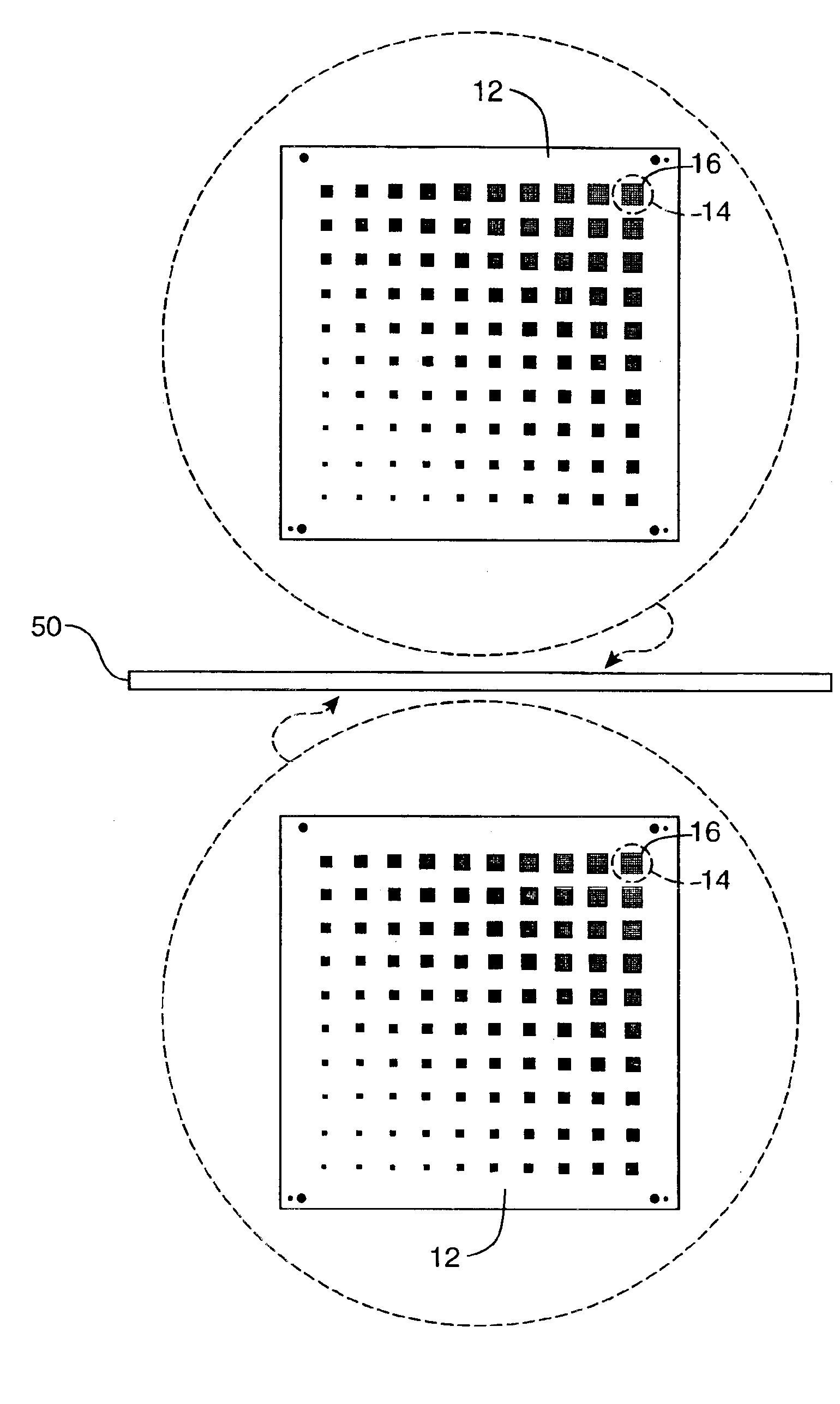
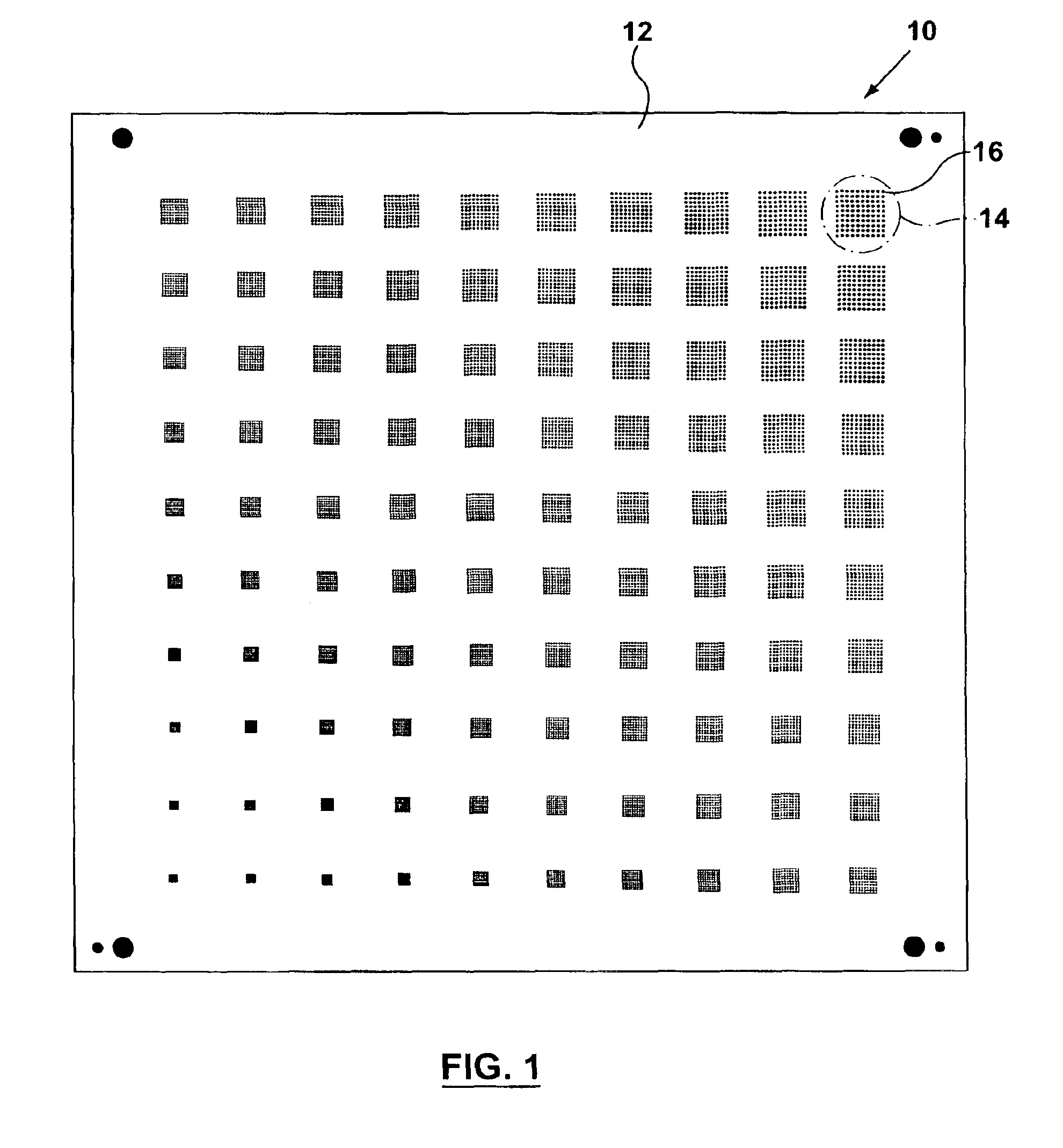
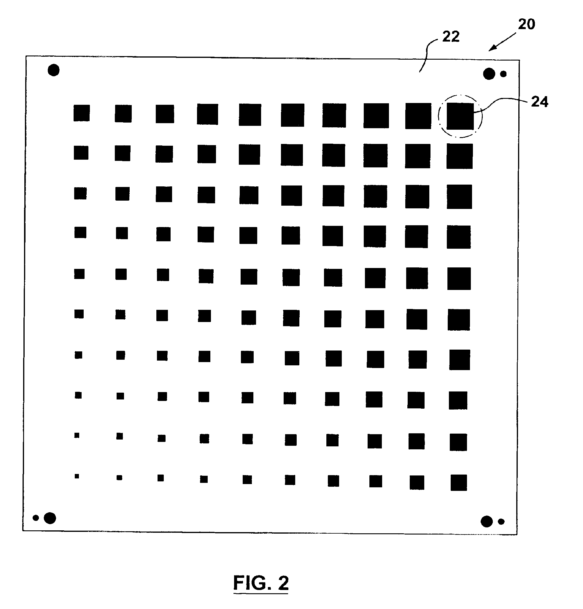
- An evaluation board with varied board pad patterns and sizes, and pad-to-pad spacings on a substrate, allowing for testing of solder paste deposition, stencil, and circuit board manufacturing processes to identify and address defects such as open pads, shorts, and voids, facilitating the evaluation of different solder paste formulations and printing/reflow parameters.


Surface mount technology evaluation board having varied board pad characteristics
PatentInactiveUS6888360B1
Innovation
- An evaluation board with varied board pad patterns and sizes, and pad-to-pad spacings on a substrate, allowing for testing of different solder paste formulations, stencil designs, and printing/reflow processes to identify and address defects, and ensure compatibility with current and future electronic component sizes.

Manufacturing Standards and Quality Control Requirements
Surface Mount Technology (SMT) implementation on substrate-like PCBs requires adherence to stringent manufacturing standards that ensure consistent product quality and reliability. The primary international standards governing SMT processes include IPC-A-610 for acceptability criteria, IPC-J-STD-001 for soldering requirements, and IPC-6012 for rigid PCB qualification specifications. These standards establish critical parameters for component placement accuracy, solder joint formation, and thermal management protocols specific to substrate-like architectures.
Manufacturing process control begins with incoming material inspection protocols that verify substrate dimensional stability, surface planarity, and thermal expansion coefficients. Component placement accuracy must maintain tolerances within ±25 micrometers for fine-pitch components, while solder paste printing requires stencil thickness optimization based on substrate thermal characteristics. Temperature profiling during reflow soldering becomes particularly critical due to the substrate's unique thermal properties, necessitating zone-specific heating curves that prevent warpage while ensuring complete solder joint formation.
Quality control frameworks incorporate both in-process monitoring and final inspection methodologies. Automated Optical Inspection (AOI) systems must be calibrated for substrate-specific reflectance properties and component visibility challenges. X-ray inspection protocols address hidden solder joint quality beneath components, particularly for Ball Grid Array (BGA) and Quad Flat No-lead (QFN) packages where traditional optical methods prove insufficient.
Statistical Process Control (SPC) implementation tracks key performance indicators including first-pass yield rates, defect density per million opportunities, and thermal cycle reliability metrics. Control charts monitor critical parameters such as solder paste volume consistency, component placement repeatability, and reflow temperature uniformity across substrate surfaces.
Traceability requirements mandate comprehensive documentation of material lots, process parameters, and inspection results throughout the manufacturing sequence. This includes substrate batch tracking, component reel identification, and environmental condition logging during assembly operations. Quality management systems must integrate these data streams to enable rapid root cause analysis and corrective action implementation when process deviations occur.
Manufacturing process control begins with incoming material inspection protocols that verify substrate dimensional stability, surface planarity, and thermal expansion coefficients. Component placement accuracy must maintain tolerances within ±25 micrometers for fine-pitch components, while solder paste printing requires stencil thickness optimization based on substrate thermal characteristics. Temperature profiling during reflow soldering becomes particularly critical due to the substrate's unique thermal properties, necessitating zone-specific heating curves that prevent warpage while ensuring complete solder joint formation.
Quality control frameworks incorporate both in-process monitoring and final inspection methodologies. Automated Optical Inspection (AOI) systems must be calibrated for substrate-specific reflectance properties and component visibility challenges. X-ray inspection protocols address hidden solder joint quality beneath components, particularly for Ball Grid Array (BGA) and Quad Flat No-lead (QFN) packages where traditional optical methods prove insufficient.
Statistical Process Control (SPC) implementation tracks key performance indicators including first-pass yield rates, defect density per million opportunities, and thermal cycle reliability metrics. Control charts monitor critical parameters such as solder paste volume consistency, component placement repeatability, and reflow temperature uniformity across substrate surfaces.
Traceability requirements mandate comprehensive documentation of material lots, process parameters, and inspection results throughout the manufacturing sequence. This includes substrate batch tracking, component reel identification, and environmental condition logging during assembly operations. Quality management systems must integrate these data streams to enable rapid root cause analysis and corrective action implementation when process deviations occur.
Thermal Management Considerations in SMT Substrate Design
Thermal management represents one of the most critical design considerations in Surface Mount Technology (SMT) implementation on substrate-like PCBs. As component densities continue to increase and power dissipation requirements grow more demanding, effective heat dissipation strategies become essential for maintaining system reliability and performance. The thermal characteristics of substrate materials directly influence the overall thermal performance of SMT assemblies.
Substrate material selection plays a fundamental role in thermal management effectiveness. Traditional FR-4 substrates exhibit relatively poor thermal conductivity, typically ranging from 0.3 to 0.4 W/mK, which creates significant thermal bottlenecks in high-power applications. Advanced substrate materials such as metal-core PCBs, ceramic substrates, and thermally enhanced laminates offer substantially improved thermal conductivity, with values reaching 1-8 W/mK for specialized materials.
Thermal via design constitutes another crucial aspect of SMT substrate thermal management. Strategic placement of thermal vias beneath high-power components creates efficient heat conduction paths from component junction to substrate ground planes or heat sinks. Via diameter, spacing, and fill materials significantly impact thermal resistance. Copper-filled vias demonstrate superior thermal performance compared to standard plated-through holes, reducing thermal resistance by approximately 30-50%.
Component placement optimization requires careful consideration of thermal interactions between adjacent SMT devices. Hot spot formation occurs when multiple high-power components cluster together without adequate thermal isolation. Thermal simulation tools enable designers to predict temperature distributions and identify potential thermal issues during the design phase, allowing for proactive thermal management strategies.
Advanced thermal management techniques include embedded cooling solutions, such as integrated heat spreaders and micro-channel cooling systems within substrate layers. These approaches enable more aggressive component packaging while maintaining acceptable operating temperatures. Thermal interface materials between components and substrates also play critical roles in minimizing thermal resistance at component-to-substrate interfaces.
Temperature cycling considerations become particularly important in SMT substrate design due to coefficient of thermal expansion mismatches between components, solder joints, and substrate materials. Proper thermal design must account for mechanical stress induced by thermal cycling to prevent solder joint fatigue and component reliability issues over extended operational lifetimes.
Substrate material selection plays a fundamental role in thermal management effectiveness. Traditional FR-4 substrates exhibit relatively poor thermal conductivity, typically ranging from 0.3 to 0.4 W/mK, which creates significant thermal bottlenecks in high-power applications. Advanced substrate materials such as metal-core PCBs, ceramic substrates, and thermally enhanced laminates offer substantially improved thermal conductivity, with values reaching 1-8 W/mK for specialized materials.
Thermal via design constitutes another crucial aspect of SMT substrate thermal management. Strategic placement of thermal vias beneath high-power components creates efficient heat conduction paths from component junction to substrate ground planes or heat sinks. Via diameter, spacing, and fill materials significantly impact thermal resistance. Copper-filled vias demonstrate superior thermal performance compared to standard plated-through holes, reducing thermal resistance by approximately 30-50%.
Component placement optimization requires careful consideration of thermal interactions between adjacent SMT devices. Hot spot formation occurs when multiple high-power components cluster together without adequate thermal isolation. Thermal simulation tools enable designers to predict temperature distributions and identify potential thermal issues during the design phase, allowing for proactive thermal management strategies.
Advanced thermal management techniques include embedded cooling solutions, such as integrated heat spreaders and micro-channel cooling systems within substrate layers. These approaches enable more aggressive component packaging while maintaining acceptable operating temperatures. Thermal interface materials between components and substrates also play critical roles in minimizing thermal resistance at component-to-substrate interfaces.
Temperature cycling considerations become particularly important in SMT substrate design due to coefficient of thermal expansion mismatches between components, solder joints, and substrate materials. Proper thermal design must account for mechanical stress induced by thermal cycling to prevent solder joint fatigue and component reliability issues over extended operational lifetimes.
Unlock deeper insights with PatSnap Eureka Quick Research — get a full tech report to explore trends and direct your research. Try now!
Generate Your Research Report Instantly with AI Agent
Supercharge your innovation with PatSnap Eureka AI Agent Platform!