

Excimer Lasers for Advanced Node Lithography: Techniques to Minimize Defects
MAY 21, 20269 MIN READ
Generate Your Research Report Instantly with AI Agent
PatSnap Eureka helps you evaluate technical feasibility & market potential.
Excimer Laser Lithography Background and Objectives
Excimer laser lithography emerged in the 1980s as a revolutionary photolithography technology, fundamentally transforming semiconductor manufacturing capabilities. The technology utilizes excimer lasers, which produce coherent ultraviolet light through excited dimers of noble gases, primarily argon fluoride (ArF) at 193nm wavelength and krypton fluoride (KrF) at 248nm wavelength. This breakthrough enabled the semiconductor industry to achieve unprecedented pattern resolution and manufacturing precision.
The evolution from mercury lamp-based proximity printing to excimer laser-based projection lithography marked a paradigmatic shift in semiconductor fabrication. Early lithography systems were limited by diffraction constraints and could only achieve feature sizes above 1 micrometer. The introduction of excimer lasers, with their shorter wavelengths and superior coherence properties, enabled the industry to break through these barriers and pursue Moore's Law scaling with greater confidence.
Advanced node lithography, typically referring to process nodes below 28nm, presents extraordinary technical challenges that demand exceptional precision and defect control. At these dimensions, even minor imperfections in the lithographic process can result in significant yield losses and performance degradation. The critical dimensions approach the fundamental limits of optical lithography, where traditional resolution enhancement techniques reach their theoretical boundaries.
The primary objective of excimer laser lithography for advanced nodes centers on achieving sub-10nm critical dimension uniformity while maintaining economically viable throughput rates. This requires sophisticated defect minimization strategies that address multiple sources of pattern distortion, including laser coherence fluctuations, optical aberrations, resist chemistry variations, and environmental instabilities. The technology must deliver consistent performance across entire wafer surfaces while accommodating increasingly complex three-dimensional device architectures.
Contemporary research focuses on extending excimer laser lithography capabilities through advanced computational lithography, multiple patterning techniques, and enhanced laser source stability. The integration of machine learning algorithms for real-time defect prediction and correction represents a significant technological frontier. Additionally, the development of next-generation photoresist materials specifically optimized for excimer laser wavelengths continues to drive improvements in pattern fidelity and defect reduction, ensuring the technology remains viable for future semiconductor generations.
Market Demand for Advanced Node Semiconductor Manufacturing
The semiconductor industry is experiencing unprecedented demand for advanced node manufacturing capabilities, driven by the proliferation of artificial intelligence, high-performance computing, and mobile technologies. Leading-edge processors for data centers, graphics processing units, and mobile system-on-chips require manufacturing processes at 7nm, 5nm, 3nm, and beyond. This technological progression necessitates increasingly sophisticated lithography systems capable of producing features with atomic-level precision.
Major semiconductor manufacturers including TSMC, Samsung, and Intel are investing heavily in advanced fabrication facilities to meet growing market demands. The transition to smaller geometries has created substantial challenges in lithography processes, where traditional light sources struggle to achieve the required resolution and pattern fidelity. Excimer lasers operating at 193nm wavelength have become critical enablers for these advanced manufacturing nodes, particularly when combined with multiple patterning techniques and immersion lithography.
The automotive industry's shift toward electric vehicles and autonomous driving systems has further amplified demand for advanced semiconductors. Power management chips, sensor processors, and AI accelerators require sophisticated manufacturing processes that depend on high-quality excimer laser lithography. Similarly, the expansion of 5G networks and Internet of Things applications has created substantial market pull for advanced node semiconductors manufactured using precise lithography techniques.
Defect minimization in excimer laser lithography has become a paramount concern as yield requirements intensify with smaller feature sizes. Even microscopic imperfections can render entire chips non-functional, making defect control techniques essential for economic viability. The market increasingly demands lithography solutions that can maintain high throughput while achieving defect densities measured in parts per billion.
Contract manufacturers and integrated device manufacturers are prioritizing suppliers who can demonstrate superior defect control capabilities in their excimer laser systems. This market dynamic has created strong incentives for developing advanced beam shaping, contamination control, and real-time monitoring technologies. The economic impact of improved defect minimization techniques extends beyond individual chip yields to encompass entire production line efficiency and time-to-market advantages.
Emerging applications in quantum computing, neuromorphic processors, and advanced memory technologies are establishing new market segments that require even more stringent lithography performance standards. These applications often demand unique device architectures and materials that challenge conventional manufacturing approaches, creating opportunities for innovative excimer laser defect minimization techniques.
Current State and Defect Challenges in Excimer Laser Systems
Excimer laser systems for advanced node lithography currently operate at 193nm wavelength using ArF (Argon Fluoride) gas mixtures, representing the backbone of sub-10nm semiconductor manufacturing processes. Leading manufacturers including Cymer (ASML subsidiary) and Gigaphoton dominate the market with laser systems capable of delivering over 90W average power at repetition rates exceeding 6kHz. These systems must maintain exceptional spectral purity with bandwidth control below 0.35pm and wavelength stability within ±0.15pm to meet the stringent requirements of extreme ultraviolet (EUV) and deep ultraviolet (DUV) lithography processes.
The primary defect challenges in current excimer laser systems stem from multiple interconnected factors that directly impact semiconductor yield and manufacturing efficiency. Optical contamination represents a critical issue, where molecular and particulate contaminants accumulate on laser chamber windows, mirrors, and beam delivery optics, causing localized absorption, scattering, and thermal distortion. These contaminants originate from gas impurities, electrode erosion products, and outgassing from chamber materials, leading to non-uniform beam profiles and intensity fluctuations that translate into pattern defects on wafers.
Spectral instability constitutes another major challenge, manifesting as wavelength drift and bandwidth broadening that compromise the precision required for advanced node patterning. Temperature variations, gas composition changes, and electrode wear contribute to spectral inconsistencies, resulting in focus errors and critical dimension variations across the exposure field. The interaction between high-energy photons and chamber materials accelerates degradation processes, creating a complex feedback loop where performance deterioration compounds over operational cycles.
Beam uniformity degradation presents significant obstacles for maintaining consistent exposure across large wafer areas. Non-uniform electrode erosion, asymmetric gas flow patterns, and optical element aging contribute to spatial intensity variations that exceed the tight tolerances required for advanced lithography. These variations manifest as across-chip linewidth variations (ACLV) and wafer-level uniformity issues that directly impact device performance and yield.
Pulse-to-pulse energy stability remains a persistent challenge, with current systems struggling to maintain energy variations below 1% RMS over extended operational periods. Factors including gas depletion, electrode conditioning, and thermal effects contribute to energy fluctuations that translate into dose variations during wafer exposure, affecting pattern fidelity and process window margins essential for advanced node manufacturing success.
Existing Defect Minimization Solutions in Laser Lithography
01 Gas discharge and electrode optimization for excimer lasers
Methods and systems for optimizing gas discharge characteristics and electrode configurations in excimer lasers to reduce operational defects. This includes techniques for improving electrode design, gas flow patterns, and discharge uniformity to minimize arcing, electrode erosion, and gas contamination that can lead to laser performance degradation.- Gas discharge and electrical system defects in excimer lasers: Defects related to the gas discharge mechanism and electrical systems in excimer lasers can significantly impact laser performance. These issues include problems with electrode degradation, gas mixture contamination, and electrical discharge instabilities that affect beam quality and output power consistency.
- Optical component degradation and alignment issues: Optical elements within excimer laser systems are susceptible to various defects including mirror coating degradation, window contamination, and misalignment problems. These defects can cause beam distortion, reduced transmission efficiency, and overall system performance deterioration over time.
- Beam quality and uniformity defects: Excimer lasers can suffer from beam quality issues including non-uniform intensity distribution, beam profile irregularities, and coherence problems. These defects affect the precision and effectiveness of laser applications, particularly in semiconductor manufacturing and medical procedures.
- Pulse stability and timing control defects: Defects in pulse generation and timing control systems can lead to inconsistent pulse energy, timing jitter, and repetition rate variations. These issues are critical for applications requiring precise temporal control and can significantly impact process quality and repeatability.
- Thermal management and cooling system failures: Thermal-related defects in excimer laser systems include inadequate cooling, temperature fluctuations, and thermal stress on components. These issues can cause wavelength drift, reduced efficiency, component damage, and shortened system lifetime, requiring proper thermal management solutions.
02 Optical component degradation and contamination control
Approaches for addressing optical component defects including window degradation, mirror contamination, and optical coating damage in excimer laser systems. These solutions focus on protective measures, cleaning techniques, and material selection to maintain optical quality and prevent beam quality deterioration over extended operation periods.Expand Specific Solutions03 Gas mixture purity and halogen management
Techniques for maintaining optimal gas mixture composition and managing halogen-related defects in excimer lasers. This includes methods for gas purification, halogen replenishment systems, and contamination prevention to ensure stable laser output and prevent performance issues caused by impure or depleted gas mixtures.Expand Specific Solutions04 Beam stability and output power control
Systems and methods for addressing beam instability and power fluctuation defects in excimer lasers. These approaches include feedback control mechanisms, power monitoring systems, and stabilization techniques to maintain consistent laser output parameters and prevent variations that could affect processing quality or system reliability.Expand Specific Solutions05 Thermal management and mechanical stability
Solutions for thermal-related defects and mechanical instabilities in excimer laser systems. This encompasses cooling system optimization, thermal stress reduction, vibration control, and structural design improvements to prevent thermal damage, mechanical misalignment, and other temperature or vibration-induced performance issues.Expand Specific Solutions
Key Players in Excimer Laser and Semiconductor Equipment Industry
The excimer laser lithography market for advanced node manufacturing represents a mature yet evolving competitive landscape. The industry is in a transitional phase, moving from traditional deep ultraviolet (DUV) excimer lasers toward extreme ultraviolet (EUV) technology for sub-7nm nodes, creating a bifurcated market worth several billion dollars annually. Technology maturity varies significantly across players, with Cymer LLC (now part of ASML) dominating the light source market through decades of ArF and KrF excimer laser development. Established semiconductor manufacturers like Intel Corp., SK Hynix, and Canon maintain strong positions in equipment integration and process optimization. Material suppliers including Tokyo Ohka Kogyo, Corning, and specialized optics companies like Carl Zeiss provide critical components for defect minimization. Emerging players from China, such as Beijing Keyi Hongyuan Optoelectronics and China Star Optoelectronics, are developing domestic capabilities, while research institutions continue advancing next-generation defect reduction techniques through improved gas purification, optical systems, and resist materials.
Cymer LLC
Technical Solution: Cymer LLC is a leading manufacturer of excimer laser light sources for semiconductor lithography, specializing in ArF and KrF excimer lasers for advanced node manufacturing. Their technology focuses on pulse energy stability control, spectral purity enhancement, and advanced gas management systems to minimize particle contamination. The company has developed sophisticated beam shaping optics and pulse-to-pulse energy control mechanisms that maintain energy variations within ±0.5% to reduce exposure uniformity defects. Their laser systems incorporate real-time wavelength monitoring and feedback control systems to ensure consistent spectral characteristics, which is critical for minimizing line edge roughness and critical dimension variations in advanced lithography processes.
Strengths: Market leader in excimer laser technology with proven track record in high-volume manufacturing, excellent pulse stability and spectral control. Weaknesses: High system complexity and maintenance requirements, significant power consumption and operational costs.
Canon, Inc.
Technical Solution: Canon develops integrated excimer laser lithography systems with advanced defect reduction techniques including sophisticated reticle inspection systems, environmental contamination control, and precision stage positioning. Their approach combines excimer laser optimization with comprehensive system-level defect management, incorporating real-time particle monitoring, advanced air filtration systems, and vibration isolation technologies. Canon's systems feature automated defect detection algorithms that can identify and compensate for various types of lithographic defects during the exposure process, significantly improving yield in advanced node production.
Strengths: Comprehensive system integration approach, strong defect detection and compensation capabilities, established semiconductor equipment manufacturer. Weaknesses: Smaller market share compared to ASML in advanced lithography, limited presence in EUV transition planning.
Core Patents in Excimer Laser Defect Reduction Technologies
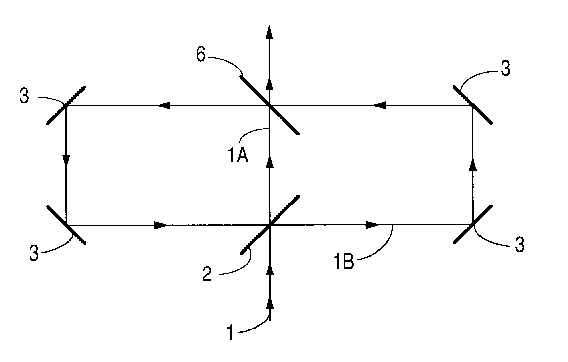
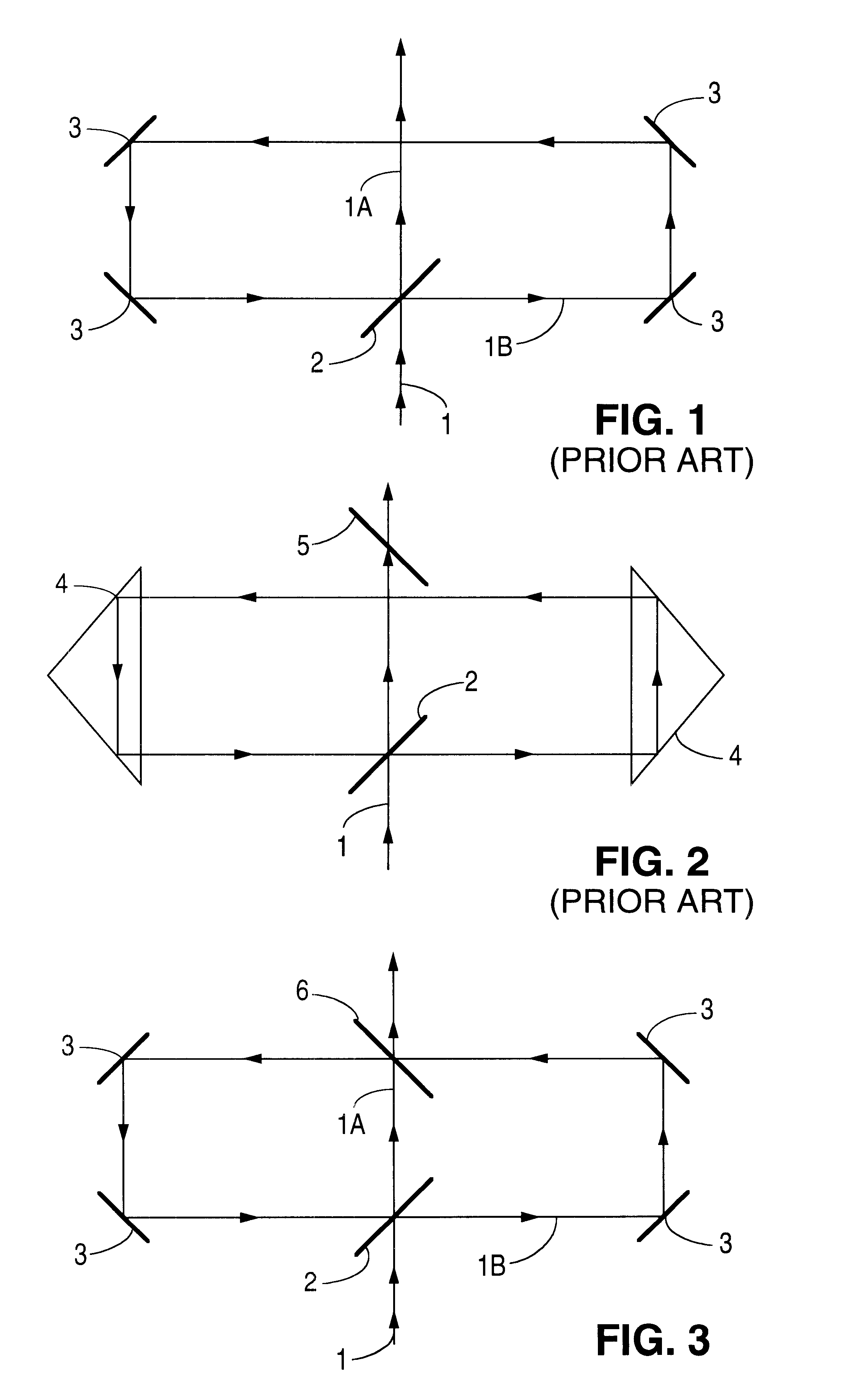
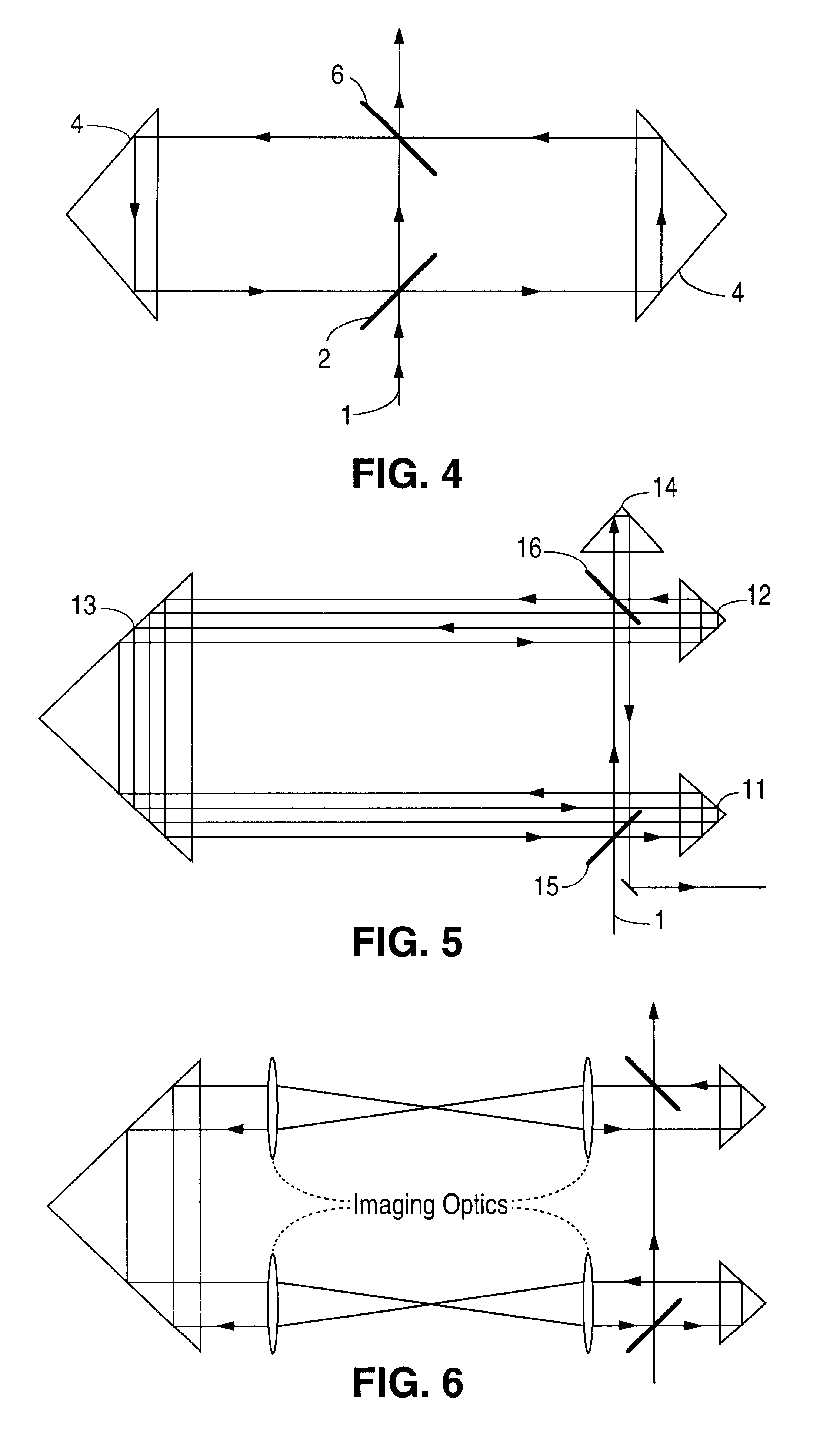
Optical pulse stretching and smoothing for ArF and F2 lithography excimer lasers
PatentInactiveUS6389045B1
Innovation
- The use of optical delay lines with multiple parallel beam paths, high reflecting coatings, and total internal reflection, along with imaging optics and multiple points of output coupling, allows for significant pulse stretching and smoothing of the temporal profile, reducing peak intensity and extending the lifetime of optical components.

Technique for efficient line narrowing of excimer lasers
PatentInactiveGB2205990A
Innovation
- The use of one or two intracavity Fabry-Perot etalons without pinholes or slits to achieve efficient line narrowing of excimer lasers, maintaining high power efficiency by tilting the etalons to prevent feedback and utilizing their transmission properties to control linewidth.


Semiconductor Industry Standards and Compliance Requirements
The semiconductor industry operates under stringent standards and compliance frameworks that directly impact excimer laser lithography systems used in advanced node manufacturing. The International Technology Roadmap for Semiconductors (ITRS) and its successor, the International Roadmap for Devices and Systems (IRDS), establish critical performance benchmarks for lithography equipment, including defect density requirements that must not exceed 0.1 defects per square centimeter for leading-edge processes.
ISO 14644 cleanroom standards mandate environmental controls essential for excimer laser operations, requiring Class 1 cleanroom conditions with particle counts below 10 particles per cubic meter for 0.1-micron and larger particles. These standards directly influence laser system design, necessitating enclosed beam paths and contamination-free optical components to prevent defect generation during exposure processes.
SEMI standards, particularly SEMI E10 for safety guidelines and SEMI E84 for equipment automation, govern excimer laser system integration within semiconductor fabs. Compliance with these standards ensures that laser wavelength stability, pulse energy uniformity, and beam coherence parameters meet the precision requirements for sub-7nm node lithography while maintaining operator safety protocols.
The FDA's Center for Devices and Radiological Health (CDRH) regulations classify excimer lasers as Class IV laser products, requiring comprehensive safety interlocks, emission controls, and documentation procedures. These compliance requirements influence system architecture, mandating redundant safety systems that can impact laser performance optimization efforts.
European CE marking requirements under the Machinery Directive 2006/42/EC and the Low Voltage Directive 2014/35/EU establish additional compliance obligations for excimer laser systems deployed in European facilities. These standards emphasize electromagnetic compatibility and electrical safety, requiring specialized filtering and shielding that can affect laser pulse characteristics and defect minimization strategies.
Quality management systems conforming to ISO 9001 and automotive-specific IATF 16949 standards increasingly influence semiconductor manufacturing, driving demand for enhanced process control and traceability in excimer laser operations, thereby establishing more rigorous defect monitoring and prevention protocols.
Environmental Impact Assessment of Excimer Laser Manufacturing
The manufacturing of excimer lasers for advanced node lithography presents significant environmental considerations that require comprehensive assessment across multiple dimensions. These high-precision optical systems, essential for producing semiconductors at sub-10nm nodes, involve complex manufacturing processes that generate various environmental impacts throughout their production lifecycle.
Energy consumption represents the most substantial environmental concern in excimer laser manufacturing. The production facilities require extensive clean room environments operating under stringent temperature, humidity, and particulate control standards. These controlled environments typically consume 10-100 times more energy per square foot compared to conventional manufacturing spaces. Additionally, the precision machining and optical component fabrication processes demand high-energy equipment operation for extended periods, contributing to substantial carbon footprint generation.
Chemical waste management poses another critical environmental challenge. Excimer laser manufacturing involves numerous hazardous materials including rare earth elements for optical coatings, specialized cleaning solvents, and photoresist chemicals. The production of high-quality optical components requires multiple etching and coating processes that generate chemical byproducts requiring specialized disposal methods. Fluorine-based gases used in excimer laser systems present particular concerns due to their high global warming potential and ozone depletion characteristics.
Water resource utilization in excimer laser manufacturing extends beyond typical industrial applications. Ultra-pure water systems essential for semiconductor-grade component cleaning consume significant volumes while generating contaminated wastewater streams. The cooling systems required for high-power laser operation and precision temperature control further amplify water consumption demands, particularly in facilities located in water-stressed regions.
Supply chain environmental impacts encompass the extraction and processing of rare materials essential for excimer laser components. Critical materials including specialized crystals, rare earth elements for optical coatings, and high-purity metals require energy-intensive extraction and refinement processes. The global distribution of these materials often necessitates long-distance transportation, adding to the overall carbon footprint of the manufacturing process.
Waste heat generation from manufacturing equipment and facility operations presents both challenges and opportunities for environmental impact mitigation. The substantial thermal loads generated during precision manufacturing processes require efficient cooling systems, while simultaneously offering potential for waste heat recovery and utilization in adjacent processes or facility heating applications.
Unlock deeper insights with PatSnap Eureka Quick Research — get a full tech report to explore trends and direct your research. Try now!
Generate Your Research Report Instantly with AI Agent
Supercharge your innovation with PatSnap Eureka AI Agent Platform!