Gallium Oxide Semiconductors in Photovoltaic Systems
OCT 27, 20259 MIN READ
Generate Your Research Report Instantly with AI Agent
Patsnap Eureka helps you evaluate technical feasibility & market potential.
Ga2O3 Semiconductor Evolution and Objectives
Gallium oxide (Ga2O3) has emerged as a promising ultra-wide bandgap semiconductor material, with its research history dating back to the 1950s. However, significant advancements in Ga2O3 semiconductor technology only began to accelerate in the early 2000s, when researchers recognized its exceptional properties for power electronics and optoelectronic applications. The material's ultra-wide bandgap of approximately 4.8-4.9 eV exceeds that of traditional semiconductors like silicon (1.1 eV), gallium nitride (3.4 eV), and silicon carbide (3.3 eV), positioning it as a next-generation semiconductor with tremendous potential.
The evolution of Ga2O3 has been marked by several key technological breakthroughs. Initially, the focus was primarily on fundamental material properties and basic growth techniques. By the 2010s, researchers had developed more sophisticated methods for producing high-quality Ga2O3 crystals, including melt growth techniques like edge-defined film-fed growth (EFG) and floating zone methods. These advancements enabled the production of larger, higher-quality substrates necessary for device fabrication.
In parallel with material development, the understanding of Ga2O3's polymorphism has expanded significantly. Among its five polymorphs (α, β, γ, δ, and ε), the β-phase has received the most attention due to its thermodynamic stability and superior electrical properties. This focus has driven research toward optimizing β-Ga2O3 for specific applications, including photovoltaic systems where its wide bandgap and high breakdown field are particularly advantageous.
The integration of Ga2O3 into photovoltaic systems represents a relatively recent development in its evolutionary trajectory. Traditional photovoltaic materials like silicon face fundamental efficiency limitations, while Ga2O3's unique properties offer pathways to overcome these barriers. Its ultra-wide bandgap makes it particularly suitable for UV detection and high-temperature operation, which are critical for specialized solar applications such as space-based solar power systems and concentrated photovoltaics.
The primary objectives for Ga2O3 semiconductor development in photovoltaic applications include enhancing conversion efficiency, improving material quality and uniformity, reducing production costs, and developing novel device architectures that leverage its unique properties. Researchers aim to optimize doping strategies to control electrical conductivity while maintaining high carrier mobility, a crucial factor for efficient photovoltaic performance.
Looking forward, the technology roadmap for Ga2O3 in photovoltaics includes developing effective heterojunction structures with complementary materials, improving contact technologies to reduce resistance losses, and exploring nanoscale engineering to enhance light absorption and carrier collection. The ultimate goal is to position Ga2O3 as a key enabling material for next-generation photovoltaic systems that can operate efficiently under extreme conditions where conventional semiconductors fail.
PV Market Demand for Wide-Bandgap Materials
The photovoltaic (PV) industry has witnessed significant growth in recent years, with global installed capacity reaching 1,013 GW by the end of 2022. This expansion has intensified the demand for more efficient and cost-effective semiconductor materials that can overcome the limitations of traditional silicon-based technologies. Wide-bandgap (WBG) materials have emerged as promising candidates for next-generation PV applications due to their superior electronic properties and potential for higher conversion efficiencies.
Market analysis indicates that the demand for WBG materials in PV applications is expected to grow at a compound annual growth rate of 25% through 2030. This growth is primarily driven by the increasing need for higher efficiency solar cells, particularly in space applications, building-integrated photovoltaics (BIPV), and regions with extreme environmental conditions where conventional silicon cells underperform.
Gallium oxide (Ga2O3), with its ultra-wide bandgap of 4.8-5.0 eV, represents a frontier material that could potentially address several market requirements. The material's exceptional breakdown field strength (8 MV/cm) and thermal stability make it particularly attractive for high-temperature and high-radiation environments where traditional semiconductors fail to maintain optimal performance.
The utility-scale solar sector, which constitutes approximately 60% of the global PV market, has shown increasing interest in WBG materials as grid parity becomes the norm in many regions. System integrators are seeking technologies that can reduce the levelized cost of electricity (LCOE) below 2 cents/kWh, a threshold where Ga2O3-based components could potentially contribute through higher conversion efficiencies and reduced balance-of-system costs.
Residential and commercial PV segments, representing about 30% of the market, are increasingly demanding aesthetically pleasing and space-efficient solutions. The transparency and potential for thin-film applications of Ga2O3 align well with these requirements, particularly for BIPV applications where form factor and visual integration are critical considerations.
Geographically, markets with high solar irradiance and extreme temperature conditions, such as the Middle East, Australia, and parts of the United States, show the strongest potential demand for WBG-based PV systems. These regions experience significant efficiency degradation in conventional silicon panels due to high operating temperatures, a challenge that Ga2O3-based systems could potentially address through better temperature coefficients.
Industry surveys indicate that 78% of PV manufacturers are exploring alternative semiconductor materials to diversify their technology portfolios, with 45% specifically investigating WBG materials. This trend is reinforced by increasing research funding, with government initiatives worldwide allocating substantial resources to advance WBG semiconductor technologies for renewable energy applications.
Ga2O3 Development Status and Technical Barriers
Gallium oxide (Ga2O3) has emerged as a promising ultra-wide bandgap semiconductor material with significant potential for power electronics and photovoltaic applications. Currently, the global research landscape shows concentrated development efforts in Japan, the United States, China, and Germany, with Japan maintaining leadership through pioneering work at institutions like the National Institute for Materials Science (NIMS) and Tamura Corporation.
The material exists in five polymorphs (α, β, γ, δ, and ε), with β-Ga2O3 receiving the most attention due to its thermodynamic stability and superior electrical properties. Recent advancements have enabled the growth of high-quality single crystals using methods such as edge-defined film-fed growth (EFG), floating zone (FZ), and Czochralski techniques, with wafer diameters reaching up to 4 inches commercially.
Despite promising progress, several critical technical barriers impede Ga2O3's widespread adoption in photovoltaic systems. The most significant challenge is its low thermal conductivity (approximately 0.1-0.3 W/cm·K), which causes heat management issues in high-power applications. This limitation becomes particularly problematic in photovoltaic systems operating under concentrated sunlight conditions.
Another major obstacle is the material's poor p-type doping capability. While n-type doping has been successfully achieved using elements like Si, Ge, and Sn, creating reliable p-type Ga2O3 remains elusive due to the deep acceptor levels and self-compensation effects. This doping asymmetry severely restricts the development of Ga2O3 homojunction devices, forcing researchers to explore heterojunction architectures that introduce additional interface challenges.
Crystal quality issues persist as well, with current growth techniques producing materials with relatively high defect densities. These defects act as recombination centers that reduce carrier lifetime and mobility, directly impacting photovoltaic efficiency. Dislocations, oxygen vacancies, and grain boundaries are particularly problematic in epitaxial layers grown for device fabrication.
The fabrication of ohmic contacts with low resistance remains challenging, especially for devices requiring high current density operation. Current metallization schemes often result in high contact resistances that limit device performance and reliability in photovoltaic applications.
From a manufacturing perspective, scaling production to commercially viable levels presents significant hurdles. Current crystal growth techniques are limited in throughput and consistency, while processing technologies for device fabrication require substantial refinement to achieve competitive yields and costs compared to established semiconductor materials.
Environmental stability is another concern, as some studies indicate potential degradation of Ga2O3 properties under prolonged UV exposure—ironically a critical consideration for photovoltaic applications. This necessitates the development of effective passivation and encapsulation techniques to ensure long-term reliability in real-world deployment scenarios.
Current Ga2O3 Integration Methods for Solar Applications
01 Gallium oxide semiconductor materials and properties
Gallium oxide (Ga2O3) is emerging as a promising wide bandgap semiconductor material with excellent electrical properties. It has a bandgap of approximately 4.8-4.9 eV, which is significantly wider than traditional semiconductors like silicon or gallium nitride. This wide bandgap gives gallium oxide superior breakdown voltage capabilities and makes it suitable for high-power electronic applications. The material also exhibits good thermal stability and can be grown in various crystalline forms, with β-Ga2O3 being the most commonly used polymorph for semiconductor applications.- Gallium oxide semiconductor device fabrication: Various methods for fabricating gallium oxide semiconductor devices, including crystal growth techniques, substrate preparation, and device structure formation. These processes are crucial for creating high-quality gallium oxide-based electronic components with optimal performance characteristics. The fabrication methods include techniques for controlling crystal orientation, doping concentration, and interface quality to achieve desired electrical properties.
- Power device applications of gallium oxide: Gallium oxide semiconductors are utilized in power electronic devices due to their wide bandgap properties, which enable high breakdown voltage and low on-resistance. These materials are particularly suitable for high-power and high-frequency applications, offering advantages over traditional silicon-based power devices. The implementation of gallium oxide in power devices allows for more efficient power conversion and management in various electronic systems.
- Doping and defect control in gallium oxide: Techniques for controlling doping levels and managing defects in gallium oxide semiconductors to optimize electrical properties. Various dopants can be incorporated to achieve n-type or p-type conductivity, while defect management strategies help improve carrier mobility and reduce unwanted recombination centers. These approaches are essential for tailoring the semiconductor properties for specific applications and enhancing overall device performance.
- Heterostructures and composite materials with gallium oxide: Development of heterostructures and composite materials incorporating gallium oxide with other semiconductor materials to create devices with enhanced functionality. These structures leverage the unique properties of gallium oxide while overcoming some of its limitations through integration with complementary materials. The resulting heterojunctions and composite systems enable novel device architectures with improved performance characteristics for various electronic and optoelectronic applications.
- Advanced processing techniques for gallium oxide semiconductors: Innovative processing methods for gallium oxide semiconductors, including novel etching techniques, surface treatments, and contact formation processes. These advanced techniques address challenges specific to gallium oxide processing, such as its chemical stability and thermal properties. The development of specialized processing approaches enables the fabrication of more complex and higher-performing gallium oxide-based devices with improved reliability and functionality.
02 Gallium oxide power devices and transistors
Gallium oxide is particularly promising for power electronic devices due to its high breakdown field strength and wide bandgap. Various transistor structures have been developed using gallium oxide, including metal-oxide-semiconductor field-effect transistors (MOSFETs), high-electron-mobility transistors (HEMTs), and junction field-effect transistors (JFETs). These devices demonstrate excellent performance characteristics such as high breakdown voltage, low on-resistance, and good switching capabilities, making them suitable for high-power and high-frequency applications in power conversion systems, electric vehicles, and renewable energy systems.Expand Specific Solutions03 Epitaxial growth and substrate technologies for gallium oxide
Various epitaxial growth techniques have been developed for gallium oxide semiconductor fabrication, including molecular beam epitaxy (MBE), metal-organic chemical vapor deposition (MOCVD), halide vapor phase epitaxy (HVPE), and mist chemical vapor deposition. These methods enable the controlled growth of high-quality gallium oxide thin films with precise doping profiles. Additionally, significant advances have been made in substrate technologies, including the development of native gallium oxide substrates and the use of alternative substrates like sapphire, silicon, and silicon carbide with appropriate buffer layers to accommodate lattice mismatches.Expand Specific Solutions04 Doping and defect engineering in gallium oxide semiconductors
Controlling the electrical properties of gallium oxide through doping and defect engineering is crucial for semiconductor device applications. N-type doping is commonly achieved using elements like silicon, tin, or germanium, while achieving effective p-type doping remains challenging due to the self-compensation effects and deep acceptor levels. Various approaches to overcome these challenges include co-doping strategies, ion implantation techniques, and defect engineering methods. Additionally, understanding and controlling native defects such as oxygen vacancies and gallium interstitials is essential for optimizing device performance and reliability.Expand Specific Solutions05 Novel device structures and applications of gallium oxide semiconductors
Beyond conventional transistors, gallium oxide is being explored for various novel device structures and applications. These include ultraviolet photodetectors that leverage the wide bandgap for solar-blind detection, Schottky barrier diodes with high breakdown voltages, gas sensors that utilize the surface properties of gallium oxide, and heterojunction devices that combine gallium oxide with other semiconductor materials. Additionally, gallium oxide is being investigated for applications in radiation-hard environments, high-temperature electronics, and as a transparent conductive oxide in optoelectronic devices, demonstrating the versatility of this semiconductor material.Expand Specific Solutions
Leading Entities in Ga2O3 Semiconductor Research
The Gallium Oxide Semiconductors market in photovoltaic systems is currently in an early growth phase, characterized by increasing research activities and emerging commercial applications. The global market is projected to expand significantly, driven by gallium oxide's superior properties including wider bandgap and higher breakdown voltage compared to traditional semiconductors. Leading players include established corporations like FLOSFIA, IBM, and ROHM Co., alongside research institutions such as Kyoto University and KAUST. The technology maturity varies across applications, with companies like NGK Insulators and Sumitomo Chemical advancing commercial viability while newer entrants like Fuga Gallium Technology focus on material development. Academic-industry partnerships, particularly involving PARC and Corning, are accelerating innovation in this promising renewable energy technology segment.
FLOSFIA, Inc.
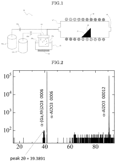
Technical Solution: FLOSFIA has pioneered the development of corundum-structured gallium oxide (α-Ga2O3) semiconductors specifically for photovoltaic applications. Their proprietary "Mist Chemical Vapor Deposition" technology enables the growth of high-quality α-Ga2O3 thin films at significantly lower temperatures than conventional methods, reducing manufacturing costs while maintaining excellent crystal quality. Their approach focuses on leveraging the wide bandgap (approximately 5.3 eV) of α-Ga2O3 to create transparent conducting layers for next-generation solar cells. FLOSFIA has demonstrated α-Ga2O3-based Schottky barrier diodes with breakdown voltages exceeding 1kV, making them suitable for high-voltage power conditioning in solar systems. Their technology also incorporates unique doping strategies to optimize carrier concentration and mobility, essential for efficient charge transport in photovoltaic applications.
Strengths: Proprietary low-temperature deposition technology reduces manufacturing costs; Corundum structure offers superior stability compared to β-Ga2O3; Excellent transparency in visible spectrum maximizes light transmission to active layers. Weaknesses: Still facing challenges in achieving large-area uniform deposition; Lower electron mobility compared to β-Ga2O3 variants; Relatively early stage of commercialization for PV-specific applications.
King Abdullah University of Science & Technology
Technical Solution: KAUST has pioneered innovative approaches to integrating gallium oxide semiconductors into next-generation photovoltaic systems through their comprehensive materials science program. Their research has developed novel synthesis methods for phase-controlled Ga2O3 nanostructures using hydrothermal techniques that achieve precise morphological control at temperatures below 200°C, significantly reducing energy requirements compared to conventional approaches. KAUST's technology incorporates unique surface functionalization strategies using phosphonic acid derivatives that create stable interfaces with organic photovoltaic materials, enabling hybrid device architectures with enhanced charge extraction. Their approach includes specialized doping protocols using transition metals that create intermediate band states within the Ga2O3 bandgap, enabling sub-bandgap photon absorption and theoretical efficiency improvements of up to 15% in tandem solar cell configurations. KAUST researchers have demonstrated Ga2O3-based transparent conducting electrodes with sheet resistances below 50 Ω/sq while maintaining over 85% transparency across the visible spectrum, creating new possibilities for top-cell contacts in multi-junction photovoltaics. Their technology also includes novel composite structures combining Ga2O3 with 2D materials like graphene and MoS2 that demonstrate enhanced charge transport properties while maintaining the environmental stability advantages of wide-bandgap oxides.
Strengths: Cutting-edge research facilities and multidisciplinary expertise in materials science; Strong focus on practical implementation and device engineering; Extensive international collaboration network accelerating technology development. Weaknesses: Early stage of technology development compared to industrial players; Limited manufacturing scale-up experience; Intellectual property commercialization pathway less defined than established companies.
Key Patents and Breakthroughs in Ga2O3 PV Technology
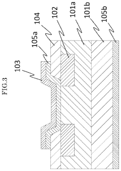
P-type oxide semiconductor and method for manufacturing same
PatentActiveUS20220352303A1
Innovation
- A method involving the generation of atomized droplets from a raw material solution containing d-block metals and Group 13 metals, carried by a carrier gas and subjected to a thermal reaction in an oxygen atmosphere to form a p-type oxide semiconductor with enhanced electrical conductivity, specifically utilizing metals like rhodium, iridium, or cobalt and indium, aluminum, or gallium to create a metal oxide with improved semiconductor properties.
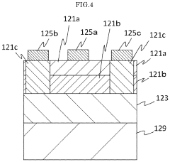
Semiconductor device
PatentPendingEP4333075A1
Innovation
- A semiconductor device is designed with a crystalline oxide semiconductor layer comprising a channel layer and a drift layer, featuring a current blocking layer with different compositions of crystalline oxides, including metals from Groups 6 to 10 and 13 of the periodic table, to enhance withstand voltage performance, utilizing a corundum structure and specific dopants for improved conductivity and insulation.
Supply Chain Analysis for Gallium-Based Materials
The global supply chain for gallium-based materials presents a complex network of extraction, processing, and distribution channels critical to the development of Gallium Oxide Semiconductors for photovoltaic applications. Gallium, primarily obtained as a byproduct of aluminum and zinc production, has limited primary sources, with China controlling approximately 95% of global production capacity. This concentration creates significant supply vulnerabilities for manufacturers in other regions.
Raw material extraction occurs predominantly in China, Australia, and Russia, with secondary sources in Germany, Kazakhstan, and Ukraine. The refining process requires specialized facilities capable of achieving the 99.99% purity levels necessary for semiconductor applications, further concentrating the supply chain among a handful of advanced processing companies.
Transportation logistics for gallium materials involve stringent requirements due to their reactive nature and high value. Special containers with inert gas environments are typically employed to prevent oxidation during transit. The COVID-19 pandemic exposed critical vulnerabilities in this supply chain, with disruptions causing price volatility exceeding 30% between 2020-2022.
Inventory management practices across the supply chain have evolved toward just-in-time models, which optimize costs but increase susceptibility to disruptions. Leading photovoltaic manufacturers typically maintain only 2-3 months of gallium oxide precursor materials in reserve, creating potential production bottlenecks during supply constraints.
Recycling infrastructure for gallium-based materials remains underdeveloped, with recovery rates below 15% globally. This represents a significant opportunity for supply chain resilience improvement, particularly as gallium oxide semiconductor deployment in photovoltaic systems increases.
Trade policies significantly impact material availability, with recent export restrictions from China affecting global markets. Tariffs ranging from 5-25% on processed gallium materials have been implemented by various countries, creating additional cost pressures for photovoltaic manufacturers utilizing gallium oxide semiconductors.
Alternative sourcing strategies are emerging, including development of gallium extraction from coal fly ash and electronic waste, which could potentially yield 300-500 metric tons annually. Several companies are also investigating gallium nitride as a potential substitute in certain applications, though its performance characteristics differ significantly from gallium oxide in photovoltaic contexts.
Environmental Impact Assessment of Ga2O3 Manufacturing
The manufacturing processes for Gallium Oxide (Ga2O3) semiconductors present significant environmental considerations that must be thoroughly evaluated as this technology advances in photovoltaic applications. Primary environmental concerns stem from gallium extraction, which typically occurs as a byproduct of aluminum and zinc processing. This extraction process requires substantial energy inputs and generates waste materials containing heavy metals and acidic compounds that can contaminate soil and water systems if improperly managed.
Chemical vapor deposition (CVD) and molecular beam epitaxy (MBE), the predominant manufacturing techniques for Ga2O3 thin films, utilize precursor gases including trimethylgallium and high-purity oxygen. These processes generate volatile organic compounds (VOCs) and particulate matter that require sophisticated abatement systems to prevent atmospheric pollution. Additionally, the high temperatures (800-1000°C) necessary for crystal growth contribute to considerable energy consumption and associated carbon emissions.
Water usage represents another critical environmental factor, with semiconductor manufacturing facilities typically consuming between 2-4 million gallons daily for wafer cleaning and processing. Wastewater from Ga2O3 production contains trace amounts of gallium, arsenic compounds, and various solvents that necessitate specialized treatment before discharge. Current recycling rates for process water in advanced facilities have reached approximately 50-60%, though industry leaders are targeting 80% recovery rates.
Life cycle assessment (LCA) studies indicate that the environmental footprint of Ga2O3 semiconductor production is currently higher per unit area than conventional silicon alternatives. However, the superior performance characteristics of Ga2O3 in high-power applications may offset these impacts through improved system efficiency over device lifetimes. Comparative analyses suggest that a Ga2O3-based photovoltaic system would need to operate approximately 1.5 times more efficiently than silicon alternatives to neutralize the additional manufacturing environmental burden.
Regulatory frameworks governing Ga2O3 manufacturing vary significantly by region, with the European Union's Restriction of Hazardous Substances (RoHS) and Registration, Evaluation, Authorization and Restriction of Chemicals (REACH) regulations imposing the strictest controls. Manufacturers in North America and Asia typically face less stringent requirements, creating potential regulatory arbitrage that may influence global production patterns.
Emerging mitigation strategies include closed-loop manufacturing systems that recover and reuse gallium, reducing raw material requirements by up to 40%. Advanced filtration technologies and catalytic oxidation systems are being implemented to reduce emissions, while research into lower-temperature synthesis methods could substantially decrease energy consumption. These improvements, coupled with renewable energy integration in manufacturing facilities, present pathways toward more sustainable Ga2O3 semiconductor production for next-generation photovoltaic applications.
Unlock deeper insights with Patsnap Eureka Quick Research — get a full tech report to explore trends and direct your research. Try now!
Generate Your Research Report Instantly with AI Agent
Supercharge your innovation with Patsnap Eureka AI Agent Platform!