

High-k Dielectrics vs Silicon Dioxide: Capacitance Comparison
MAY 13, 20269 MIN READ
Generate Your Research Report Instantly with AI Agent
PatSnap Eureka helps you evaluate technical feasibility & market potential.
High-k Dielectric Development Background and Objectives
The semiconductor industry's relentless pursuit of device miniaturization has driven continuous evolution in dielectric materials for over five decades. Silicon dioxide (SiO2) served as the cornerstone gate dielectric material since the early days of MOSFET technology, enabling the remarkable scaling achievements predicted by Moore's Law. However, as transistor dimensions approached the nanoscale regime in the early 2000s, fundamental physical limitations of SiO2 became increasingly apparent, necessitating a paradigm shift toward alternative dielectric solutions.
The primary challenge emerged when SiO2 gate dielectric thickness scaled below 2 nanometers, corresponding to approximately 5-6 atomic layers. At these dimensions, quantum mechanical tunneling effects became dominant, causing exponential increases in gate leakage current that severely compromised device performance and power efficiency. This phenomenon, known as direct tunneling, created an insurmountable barrier to further scaling using conventional SiO2-based approaches.
High-k dielectric materials emerged as the most viable solution to overcome these scaling limitations while maintaining essential electrical performance characteristics. The term "high-k" refers to materials possessing dielectric constants significantly higher than SiO2's value of 3.9. By incorporating materials with dielectric constants ranging from 10 to over 100, engineers could achieve equivalent electrical thickness while using physically thicker layers, thereby dramatically reducing tunneling leakage.
The development objectives for high-k dielectrics encompass multiple critical requirements beyond simply achieving high dielectric constants. Thermal stability represents a fundamental prerequisite, as these materials must withstand processing temperatures exceeding 1000°C without degradation or unwanted interfacial reactions. Interface quality with silicon substrates demands careful optimization to minimize charge trapping and maintain carrier mobility. Additionally, compatibility with existing semiconductor manufacturing processes ensures practical implementation without requiring complete fabrication infrastructure overhaul.
The strategic importance of high-k dielectric development extends beyond immediate scaling solutions, positioning these materials as enablers for next-generation device architectures including FinFETs, gate-all-around transistors, and emerging memory technologies. This technological transition represents one of the most significant materials innovations in semiconductor history, fundamentally reshaping the landscape of modern electronics manufacturing.
Market Demand for Advanced Semiconductor Capacitors
The semiconductor industry is experiencing unprecedented demand for advanced capacitor technologies, driven primarily by the continuous miniaturization of electronic devices and the exponential growth in computing performance requirements. As transistor dimensions shrink below the 22-nanometer node, traditional silicon dioxide gate dielectrics face fundamental physical limitations that compromise device performance and reliability. This technological bottleneck has created substantial market pressure for alternative dielectric materials with superior electrical properties.
Mobile computing devices represent the largest market segment driving demand for high-k dielectric capacitors. Smartphones, tablets, and wearable electronics require processors that deliver enhanced performance while maintaining strict power consumption constraints. The proliferation of artificial intelligence applications at the edge, including real-time image processing and natural language processing, necessitates memory and logic circuits with significantly improved capacitance density and reduced leakage currents.
Data center infrastructure constitutes another critical market driver, as cloud computing services and enterprise applications demand increasingly powerful server processors. The exponential growth in data processing requirements, particularly for machine learning workloads and big data analytics, has intensified the need for memory technologies that can support higher bandwidth and lower latency operations. Advanced capacitor technologies enable the development of high-performance cache memories and embedded DRAM solutions essential for next-generation server architectures.
The automotive electronics sector presents emerging opportunities for advanced semiconductor capacitors, particularly with the rapid adoption of electric vehicles and autonomous driving systems. Advanced driver assistance systems require sophisticated sensor fusion capabilities and real-time processing power that depend on high-performance semiconductor devices with superior capacitive properties.
Market dynamics indicate strong growth potential across multiple application domains, with particular emphasis on technologies that can simultaneously address performance, power efficiency, and manufacturing scalability requirements. The transition from silicon dioxide to high-k dielectric materials represents a fundamental shift in semiconductor manufacturing, creating substantial opportunities for companies that can successfully develop and commercialize these advanced capacitor technologies.
Current Status and Challenges of High-k vs SiO2 Technologies
The semiconductor industry currently faces a critical transition period regarding gate dielectric materials, with high-k dielectrics emerging as the primary successor to traditional silicon dioxide (SiO2) in advanced CMOS technologies. Silicon dioxide has served as the industry standard for decades due to its excellent interface properties with silicon, thermal stability, and well-established manufacturing processes. However, as device scaling continues below the 65nm technology node, SiO2 encounters fundamental physical limitations that threaten Moore's Law continuation.
The primary challenge with SiO2 stems from quantum mechanical tunneling effects that become pronounced when oxide thickness approaches 1-2 nanometers. At these dimensions, gate leakage current increases exponentially, leading to unacceptable power consumption and device reliability issues. This physical barrier has necessitated the adoption of high-k materials such as hafnium dioxide (HfO2), aluminum oxide (Al2O3), and various hafnium-based compounds that can provide equivalent electrical thickness while maintaining greater physical thickness.
High-k dielectrics currently dominate in sub-32nm processes, with HfO2-based materials being the most commercially successful. Major foundries including TSMC, Samsung, and Intel have successfully integrated high-k/metal gate stacks into their production lines. However, several technical challenges persist in high-k implementation, including threshold voltage instability, mobility degradation due to remote phonon scattering, and interface trap density issues that affect device performance and reliability.
Manufacturing complexity represents another significant challenge, as high-k materials require precise atomic layer deposition (ALD) processes and careful thermal budget management to prevent crystallization and maintain amorphous structure. The integration with metal gates adds additional complexity, requiring new materials engineering approaches and process optimization to achieve desired work function tuning and minimize interface reactions.
Reliability concerns continue to challenge high-k adoption, particularly regarding bias temperature instability (BTI) and time-dependent dielectric breakdown (TDDB) mechanisms that differ significantly from SiO2 behavior. These phenomena require extensive characterization and new reliability models to ensure long-term device operation in commercial applications.
Despite these challenges, the industry has achieved remarkable progress in high-k integration, with current technologies demonstrating acceptable performance metrics for most applications. The ongoing development focuses on advanced high-k materials, interface engineering techniques, and novel device architectures to address remaining limitations while enabling continued scaling toward sub-10nm technologies.
Current High-k Dielectric Integration Solutions
01 High-k dielectric materials for enhanced capacitance
Advanced dielectric materials with high dielectric constants are utilized to significantly increase capacitance values in electronic devices. These materials enable the development of smaller capacitors with higher energy storage capabilities, improving overall device performance and miniaturization. The high-k materials provide superior electrical properties compared to traditional dielectric materials.- High-k dielectric materials for enhanced capacitance: Advanced dielectric materials with high dielectric constants are utilized to significantly increase capacitance values in electronic devices. These materials enable the development of compact capacitors with superior electrical performance by providing enhanced charge storage capabilities while maintaining device miniaturization requirements.
- Thin film deposition techniques for high-k dielectrics: Specialized deposition methods are employed to create uniform thin films of high-k dielectric materials with precise thickness control. These techniques ensure optimal electrical properties and interface quality, which are critical for achieving maximum capacitance performance in semiconductor applications.
- Metal-insulator-metal capacitor structures: Capacitor architectures utilizing metal electrodes separated by high-k dielectric layers are designed to maximize capacitance density. These structures optimize the electric field distribution and minimize leakage current while providing stable electrical characteristics across various operating conditions.
- Interface engineering and surface treatment: Surface modification techniques and interface optimization methods are applied to improve the electrical properties of high-k dielectric layers. These approaches reduce interface defects, enhance dielectric strength, and ensure reliable capacitor performance through controlled surface chemistry and atomic-level engineering.
- Multi-layer and composite dielectric systems: Complex dielectric structures incorporating multiple layers or composite materials are developed to achieve enhanced capacitance characteristics. These systems combine different dielectric materials with complementary properties to optimize overall electrical performance while addressing specific application requirements.
02 Thin film deposition techniques for high-k dielectrics
Specialized deposition methods are employed to create uniform thin films of high-k dielectric materials with precise thickness control. These techniques ensure optimal electrical characteristics and reliability of the dielectric layers. The deposition processes are critical for achieving consistent performance across large-scale manufacturing.Expand Specific Solutions03 Metal gate integration with high-k dielectrics
The combination of metal gate electrodes with high-k dielectric materials creates enhanced capacitor structures with improved electrical performance. This integration addresses compatibility issues and optimizes the interface properties between the gate and dielectric layers. The approach enables better control over threshold voltages and reduces leakage currents.Expand Specific Solutions04 Multilayer dielectric stack configurations
Complex multilayer structures incorporating different dielectric materials are designed to optimize capacitance while maintaining electrical stability. These configurations allow for fine-tuning of electrical properties through careful selection and arrangement of dielectric layers. The multilayer approach provides enhanced performance characteristics and improved reliability.Expand Specific Solutions05 Process optimization for high-k capacitor manufacturing
Manufacturing processes are specifically tailored to address the unique challenges associated with high-k dielectric materials. These optimizations include thermal treatment procedures, interface engineering, and contamination control measures. The refined processes ensure consistent quality and performance of the final capacitor devices while maintaining cost-effectiveness in production.Expand Specific Solutions
Major Players in High-k Dielectric and Silicon Processing
The high-k dielectrics versus silicon dioxide capacitance comparison represents a mature technology segment within the advanced semiconductor manufacturing industry, currently valued at approximately $15-20 billion globally and experiencing steady 5-7% annual growth driven by continued device scaling demands. The competitive landscape is dominated by established semiconductor giants including Taiwan Semiconductor Manufacturing Co., Samsung Electronics, and GlobalFoundries, who have successfully integrated high-k materials like hafnium oxide into their advanced process nodes below 45nm. Technology maturity varies significantly across players, with TSMC and Samsung leading in high-volume manufacturing implementation, while companies like Micron Technology and SK Hynix focus on memory-specific applications. Foundry services providers such as United Microelectronics and Semiconductor Manufacturing International are actively developing capabilities, though trailing the technology leaders by 1-2 generations in advanced high-k integration sophistication.
Taiwan Semiconductor Manufacturing Co., Ltd.
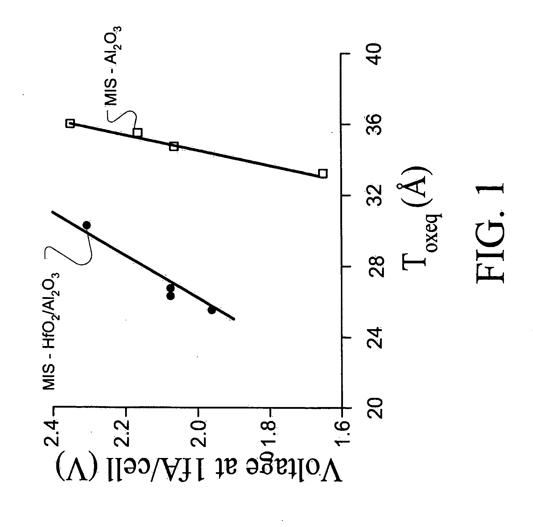
Technical Solution: TSMC has extensively developed high-k dielectric materials including hafnium oxide (HfO2) and hafnium silicate for advanced node processes. Their high-k/metal gate technology implementation began at 45nm node and has been continuously refined through 7nm and 5nm processes. The company utilizes atomic layer deposition (ALD) techniques to achieve precise thickness control of high-k layers, typically 1-3nm thick, which provides significantly higher capacitance density compared to silicon dioxide while maintaining low leakage current. TSMC's high-k dielectrics achieve dielectric constants of 15-25 compared to SiO2's 3.9, enabling continued transistor scaling and improved performance in mobile and high-performance computing applications.
Strengths: Industry-leading manufacturing capability and yield optimization for high-k materials. Weaknesses: Higher manufacturing complexity and cost compared to traditional SiO2 processes.
Micron Technology, Inc.
Technical Solution: Micron has developed specialized high-k dielectric technologies primarily for memory applications, focusing on materials that enhance capacitance density in DRAM and emerging memory technologies. Their high-k implementation includes titanium oxide, hafnium oxide, and composite high-k stacks that provide superior capacitance characteristics compared to traditional silicon dioxide or silicon nitride dielectrics. Micron's high-k solutions achieve dielectric constants of 10-40 depending on the specific material composition and application requirements. The company has successfully integrated these materials into their 3D NAND and advanced DRAM processes, enabling continued scaling and improved storage density. Their approach includes careful optimization of deposition conditions and post-processing treatments to achieve the required electrical performance and reliability standards for memory applications.
Strengths: Specialized expertise in memory-optimized high-k materials with proven reliability. Weaknesses: Primarily focused on memory applications rather than general logic device optimization.
Core Patents in High-k Dielectric Capacitance Enhancement
Process for deposition of a thin layer on an oxidized layer of a substrate
PatentInactiveUS7030043B2
Innovation
- Incorporating a densification sequence after each atomic layer deposition, which includes a longer purging step, an additional injection of the second reagent, and another purging step, with extended time durations compared to the standard reaction cycle, to control the interfacial layer growth and stabilize the thin layer.


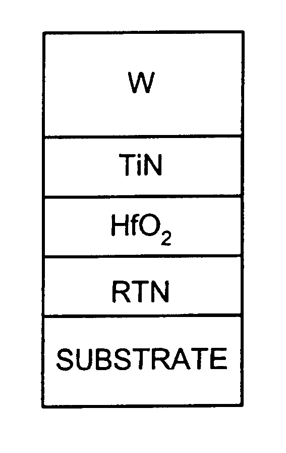
High performance MIS capacitor with HfO2 dielectric
PatentInactiveUS20050070063A1
Innovation
- A method involving atomic layer deposition (ALD) of hafnium oxide using an organic hafnium precursor, followed by repeated oxidation treatments with oxidants like O3 to reduce carbon contamination and minimize crystallization, while maintaining low thermal budgets to prevent degradation, is employed. This process forms a high-purity HfO2 layer with improved scalability and reduced leakage currents.

Manufacturing Process Compatibility and Scalability
The manufacturing process compatibility between high-k dielectrics and silicon dioxide represents a critical consideration in semiconductor fabrication scalability. Silicon dioxide has established itself as the gold standard due to its seamless integration with existing CMOS manufacturing processes. The material exhibits excellent thermal stability during standard annealing processes, typically withstanding temperatures up to 1000°C without significant degradation. Its chemical compatibility with silicon substrates ensures minimal interface state density and reliable electrical performance.
High-k dielectrics present more complex manufacturing challenges that directly impact scalability. Materials such as hafnium oxide (HfO₂) and aluminum oxide (Al₂O₃) require modified deposition techniques, including atomic layer deposition (ALD) and chemical vapor deposition (CVD), which operate at lower temperatures compared to silicon dioxide processing. These materials are sensitive to high-temperature annealing, often experiencing crystallization and phase transitions that can degrade their dielectric properties.
The integration of high-k materials necessitates significant modifications to existing fabrication workflows. Traditional gate stack formation processes must be adapted to accommodate the different thermal budgets and chemical sensitivities of high-k dielectrics. This includes adjustments to dopant activation annealing, metal gate electrode deposition, and subsequent processing steps. The requirement for interfacial layers between high-k materials and silicon substrates adds additional complexity to the manufacturing sequence.
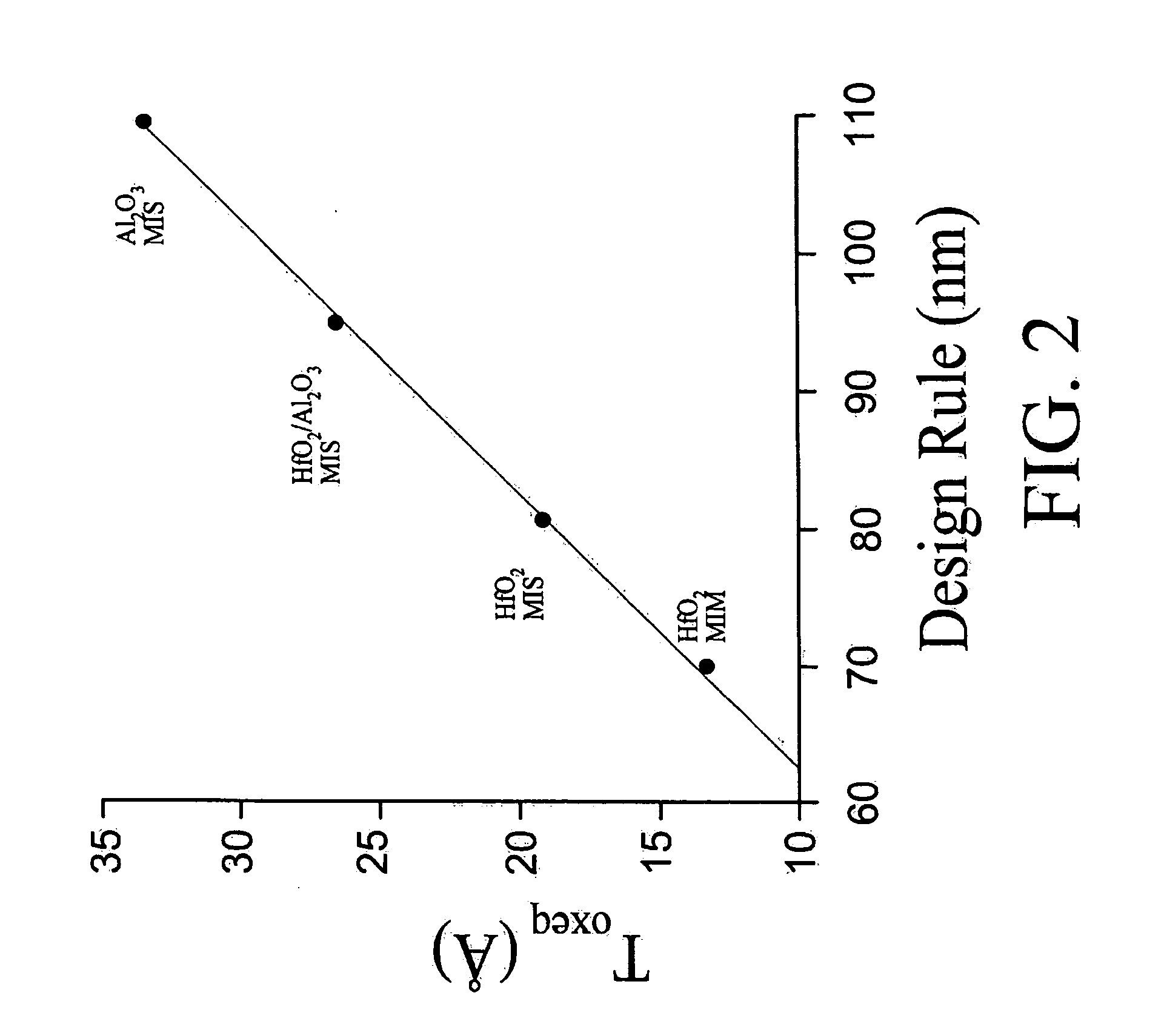
Scalability considerations reveal distinct advantages for each approach. Silicon dioxide benefits from mature, high-throughput manufacturing processes with established yield optimization strategies. The material's compatibility with existing equipment and process flows enables cost-effective scaling to high-volume production. However, its fundamental physical limitations in advanced technology nodes create scalability constraints for future device generations.
High-k dielectrics offer superior scalability for advanced nodes despite manufacturing complexity. The ability to achieve equivalent electrical thickness with greater physical thickness provides enhanced process control and reduced variability. Modern ALD systems have demonstrated excellent uniformity and repeatability for high-k deposition across large wafer areas, supporting volume manufacturing requirements. The initial investment in process development and equipment modification is offset by the extended roadmap capability these materials provide for continued device scaling.
High-k dielectrics present more complex manufacturing challenges that directly impact scalability. Materials such as hafnium oxide (HfO₂) and aluminum oxide (Al₂O₃) require modified deposition techniques, including atomic layer deposition (ALD) and chemical vapor deposition (CVD), which operate at lower temperatures compared to silicon dioxide processing. These materials are sensitive to high-temperature annealing, often experiencing crystallization and phase transitions that can degrade their dielectric properties.
The integration of high-k materials necessitates significant modifications to existing fabrication workflows. Traditional gate stack formation processes must be adapted to accommodate the different thermal budgets and chemical sensitivities of high-k dielectrics. This includes adjustments to dopant activation annealing, metal gate electrode deposition, and subsequent processing steps. The requirement for interfacial layers between high-k materials and silicon substrates adds additional complexity to the manufacturing sequence.
Scalability considerations reveal distinct advantages for each approach. Silicon dioxide benefits from mature, high-throughput manufacturing processes with established yield optimization strategies. The material's compatibility with existing equipment and process flows enables cost-effective scaling to high-volume production. However, its fundamental physical limitations in advanced technology nodes create scalability constraints for future device generations.
High-k dielectrics offer superior scalability for advanced nodes despite manufacturing complexity. The ability to achieve equivalent electrical thickness with greater physical thickness provides enhanced process control and reduced variability. Modern ALD systems have demonstrated excellent uniformity and repeatability for high-k deposition across large wafer areas, supporting volume manufacturing requirements. The initial investment in process development and equipment modification is offset by the extended roadmap capability these materials provide for continued device scaling.
Reliability and Performance Trade-offs Analysis
The transition from silicon dioxide to high-k dielectrics in semiconductor manufacturing presents a complex landscape of reliability and performance trade-offs that fundamentally reshape device characteristics. While high-k materials offer superior capacitance density enabling continued scaling, they introduce new failure mechanisms and performance considerations that require careful evaluation against traditional SiO2 benchmarks.
Reliability challenges emerge as primary concerns when implementing high-k dielectrics. These materials exhibit increased susceptibility to charge trapping phenomena, leading to threshold voltage instability and reduced device lifetime. Interface defect densities at high-k/silicon boundaries typically exceed those of SiO2/silicon interfaces by orders of magnitude, creating additional leakage paths and degradation mechanisms. Temperature-induced stress effects become more pronounced, with high-k materials showing accelerated aging under thermal cycling conditions compared to silicon dioxide's proven thermal stability.
Performance trade-offs manifest across multiple operational parameters. High-k dielectrics demonstrate superior gate control and reduced short-channel effects due to enhanced capacitive coupling, enabling aggressive device scaling. However, carrier mobility degradation occurs due to increased interface roughness and remote phonon scattering, potentially offsetting speed improvements. Power consumption characteristics shift significantly, with reduced gate leakage current improving static power while altered switching characteristics may impact dynamic power efficiency.
Process integration complexities introduce additional reliability considerations. High-k materials require modified deposition and annealing processes that can introduce contamination risks and interface quality variations. Thermal budget constraints limit processing flexibility, potentially compromising other device parameters. Chemical compatibility issues with existing metallization and interconnect materials create new failure modes not present in SiO2-based systems.
Long-term reliability assessment reveals divergent behavior patterns between high-k and SiO2 systems. While silicon dioxide exhibits well-characterized wear-out mechanisms with predictable failure distributions, high-k materials show more complex degradation patterns influenced by material composition, interface engineering, and processing conditions. This complexity necessitates extended qualification periods and modified reliability testing protocols to ensure adequate product lifetime predictions.
Unlock deeper insights with PatSnap Eureka Quick Research — get a full tech report to explore trends and direct your research. Try now!
Generate Your Research Report Instantly with AI Agent
Supercharge your innovation with PatSnap Eureka AI Agent Platform!