

High-Speed Optical Transceiver Design Using Silicon Photonics
OCT 14, 20259 MIN READ
Generate Your Research Report Instantly with AI Agent
PatSnap Eureka helps you evaluate technical feasibility & market potential.
Silicon Photonics Evolution and Objectives
Silicon photonics has evolved significantly since its inception in the late 1980s, transforming from an academic curiosity to a commercial reality. The technology leverages the mature CMOS fabrication infrastructure to integrate optical components on silicon substrates, enabling unprecedented levels of integration and cost reduction. Early developments focused on basic passive components such as waveguides and couplers, while recent advancements have successfully demonstrated active components including modulators, photodetectors, and even lasers on silicon platforms.
The evolution trajectory shows three distinct phases: exploration (1990s-2000s), development (2000s-2010s), and commercialization (2010s-present). During the exploration phase, researchers established fundamental principles and demonstrated basic functionalities. The development phase witnessed significant improvements in component performance and reliability, while the current commercialization phase is characterized by industrial adoption and volume production.
A critical milestone was reached in 2015 when several companies began shipping silicon photonics-based transceivers for data center applications. This marked the transition from research to practical implementation, validating the technology's commercial viability. Since then, data rates have increased from 100 Gbps to 400 Gbps, with 800 Gbps and 1.6 Tbps solutions under development.
The primary objective of silicon photonics in high-speed optical transceiver design is to overcome the bandwidth limitations of traditional copper interconnects while maintaining cost-effectiveness and scalability. Specific technical goals include achieving data rates exceeding 1 Tbps per channel, reducing power consumption below 1 pJ/bit, minimizing footprint to enable higher integration density, and ensuring compatibility with existing optical network infrastructure.
Another crucial objective is to address the "interconnect bottleneck" in computing systems, where data movement between chips and boards increasingly limits overall system performance. Silicon photonics promises to alleviate this constraint by enabling optical connections directly to or even within processor packages.
Looking forward, the technology aims to support emerging applications such as artificial intelligence, quantum computing, and autonomous vehicles, all of which require unprecedented bandwidth and latency performance. The ultimate vision is to create fully integrated electro-optical systems where light generation, manipulation, and detection occur seamlessly on a single chip, revolutionizing how we build computing and communication systems.
The convergence of silicon photonics with other advanced technologies, including 3D packaging, specialized ASICs, and novel materials like graphene and other 2D materials, represents the frontier of research in this domain, promising even greater performance improvements in the coming decade.
Market Analysis for High-Speed Optical Interconnects
The global market for high-speed optical interconnects is experiencing unprecedented growth, driven primarily by escalating data traffic demands across various sectors. Data centers represent the largest market segment, with their bandwidth requirements doubling approximately every two years. This exponential growth is fueled by cloud computing services, video streaming platforms, and emerging applications like artificial intelligence and machine learning that require massive data processing capabilities.
Telecommunications forms another significant market segment, particularly with the ongoing deployment of 5G networks worldwide. The transition to 5G has necessitated substantial upgrades to optical backhaul infrastructure, creating sustained demand for high-speed optical interconnects capable of supporting multi-gigabit data rates with minimal latency.
Enterprise networks constitute a growing market as businesses increasingly migrate to cloud-based operations and implement data-intensive applications. This transition has created demand for higher bandwidth connections between corporate data centers and cloud service providers, driving adoption of optical interconnect technologies.
The consumer electronics sector represents an emerging opportunity, with high-definition content streaming, virtual reality, and augmented reality applications requiring increasingly robust data transmission capabilities. While currently smaller than other segments, this market shows promising growth potential as these technologies become more mainstream.
Geographically, North America leads the market due to its concentration of data center operators, cloud service providers, and technology companies. The Asia-Pacific region follows closely, showing the fastest growth rate driven by rapid digital transformation in countries like China, Japan, South Korea, and India. Europe maintains a significant market share, particularly in telecommunications applications.
Market forecasts indicate the global optical interconnect market will maintain a compound annual growth rate exceeding 15% through 2028. Silicon photonics-based solutions are projected to grow at an even higher rate due to their advantages in integration, power efficiency, and cost-effectiveness at scale.
Key market drivers include the exponential growth in global IP traffic, increasing adoption of cloud services, the proliferation of connected devices, and the emergence of data-intensive applications. Additionally, energy efficiency concerns in data centers are accelerating the transition from copper to optical interconnects, as optical solutions offer significantly lower power consumption per bit transmitted.
Market restraints include high initial implementation costs, technical challenges in achieving seamless integration with existing infrastructure, and competition from alternative technologies in certain application segments.
Silicon Photonics State-of-Art and Barriers
Silicon photonics has emerged as a transformative technology in the field of optical communications, enabling the integration of photonic components with electronic circuits on silicon substrates. Currently, the state-of-the-art in silicon photonics demonstrates impressive capabilities, with data rates exceeding 100 Gbps per channel and integration densities allowing thousands of photonic components on a single chip. Leading research institutions and companies have achieved modulation speeds up to 50-70 GHz, insertion losses below 1 dB for passive components, and photodetector responsivities approaching 1 A/W.
Despite these advancements, significant barriers remain in the widespread adoption of silicon photonics for high-speed optical transceivers. One fundamental challenge is silicon's indirect bandgap, which limits its light emission efficiency. This necessitates the integration of III-V materials for laser sources, creating complex heterogeneous integration challenges and increasing manufacturing costs. Current hybrid integration approaches still struggle with coupling efficiency, thermal management, and long-term reliability.
Thermal sensitivity presents another critical barrier, as silicon photonic devices typically exhibit temperature-dependent wavelength shifts of approximately 70-80 pm/°C. This necessitates precise temperature control systems or athermal design approaches, adding complexity and power consumption to transceiver designs. The implementation of efficient thermal compensation techniques without compromising performance remains challenging.
Coupling losses between optical fibers and silicon waveguides continue to be problematic, with typical edge coupling losses of 3-5 dB per facet. While grating couplers offer an alternative approach, they introduce wavelength dependency and polarization sensitivity. Advanced edge coupling techniques using spot-size converters can reduce losses to 1-2 dB but add fabrication complexity.
Manufacturing variability across wafers affects critical dimensions of photonic components, leading to performance deviations in resonant structures and phase-sensitive devices. Current processes show variations of ±5-10 nm in waveguide dimensions, necessitating active tuning mechanisms that increase power consumption and control complexity.
Packaging remains perhaps the most significant barrier to commercial scaling. The need for precise optical alignment (typically sub-micron), hermetic sealing, and electrical-optical interfaces dramatically increases assembly costs. Current packaging approaches can represent 60-80% of the total device cost, limiting mass-market adoption.
The integration of electronic and photonic components also faces challenges related to process compatibility, signal integrity at high frequencies, and thermal management. While monolithic integration offers the highest potential performance, the compromises required in process optimization often result in sub-optimal performance for both electronic and photonic components.
Current High-Speed Transceiver Architectures
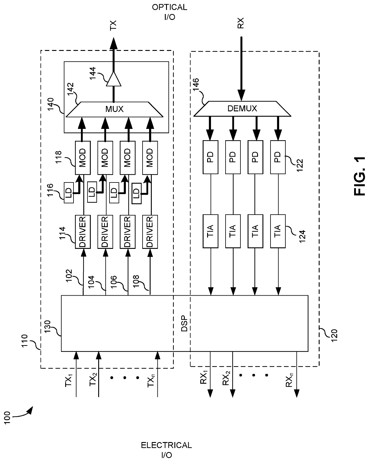
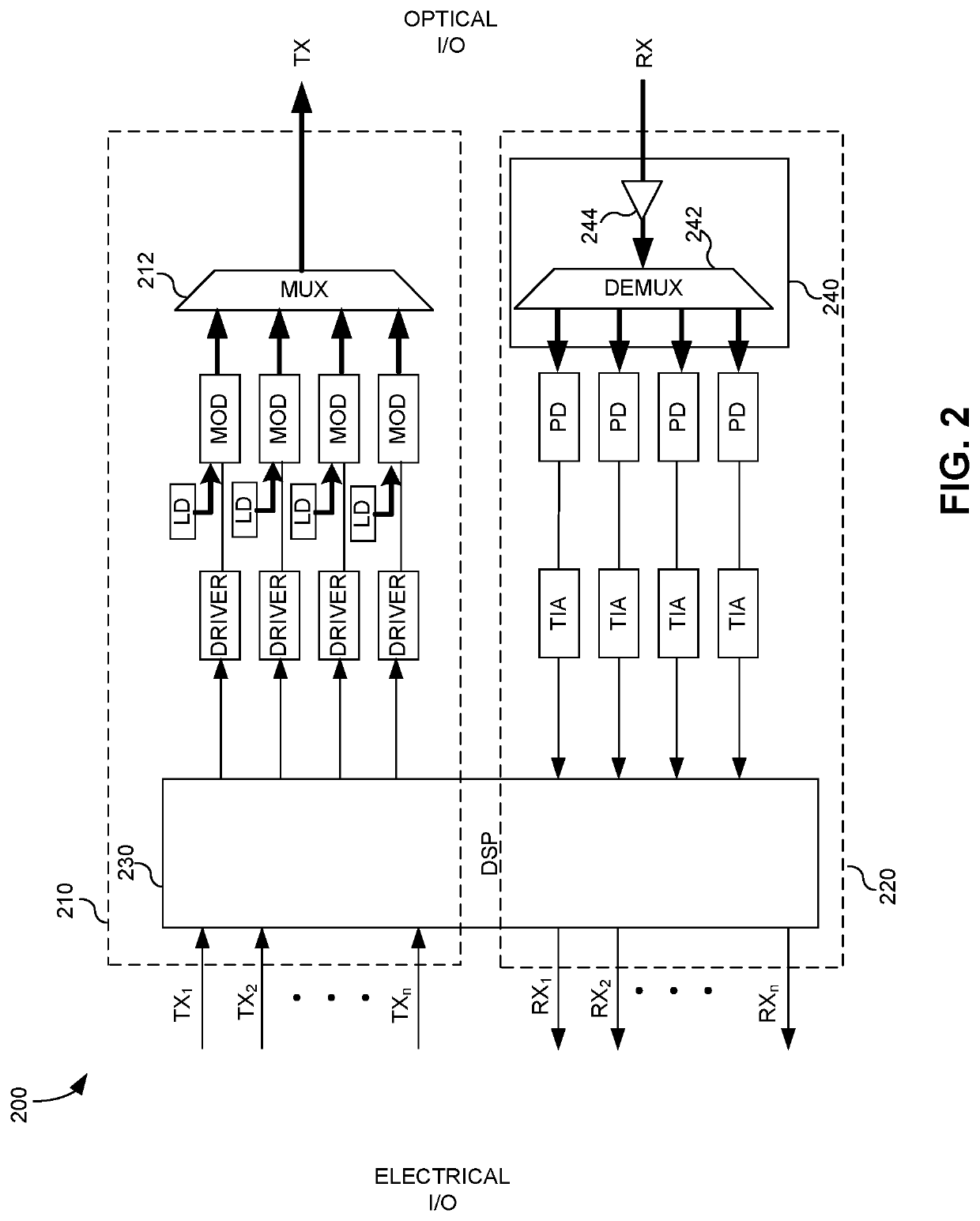
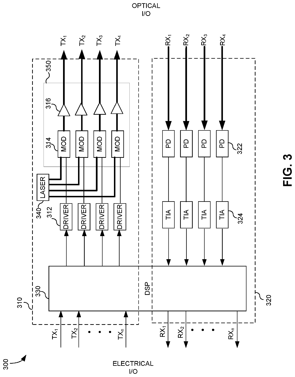
01 High-speed silicon photonic integrated circuits for optical transceivers
Silicon photonic integrated circuits enable high-speed optical transceivers by integrating multiple photonic components on a single chip. These circuits incorporate waveguides, modulators, and photodetectors to achieve data rates exceeding 100 Gbps. The integration of silicon photonics technology allows for reduced power consumption, smaller form factors, and enhanced bandwidth compared to traditional optical communication systems.- High-speed silicon photonic transceivers: Silicon photonic transceivers can achieve high data transmission speeds by integrating optical components on silicon substrates. These transceivers utilize advanced modulation techniques and efficient coupling mechanisms to enable data rates exceeding 100 Gbps. The integration of multiple optical channels on a single chip allows for parallel data transmission, further increasing the overall bandwidth capacity while maintaining compact form factors suitable for data center applications.
- Integration of silicon photonics with electronic components: The integration of silicon photonic elements with electronic components enables high-performance optical transceivers. By combining CMOS-compatible photonic devices with electronic drivers and receivers on the same chip or package, signal integrity is improved while power consumption and latency are reduced. This hybrid integration approach facilitates seamless conversion between electrical and optical signals, enhancing overall transceiver performance and enabling higher data transmission speeds.
- Waveguide structures for improved optical transmission: Advanced waveguide structures are crucial for enhancing the performance of silicon photonic transceivers. These structures include strip waveguides, rib waveguides, and subwavelength gratings that minimize propagation losses and enable efficient light transmission. Specialized waveguide designs can support multiple optical modes, reduce crosstalk between adjacent channels, and facilitate coupling between different photonic components, all contributing to increased data transmission speeds in optical transceivers.
- Modulation techniques for silicon photonic transceivers: Various modulation techniques are employed in silicon photonic transceivers to increase data transmission speeds. These include phase-shift keying (PSK), quadrature amplitude modulation (QAM), and pulse amplitude modulation (PAM). Silicon-based modulators utilizing the plasma dispersion effect or electro-absorption mechanisms can achieve high modulation bandwidths. Advanced modulation formats combined with efficient signal processing enable higher spectral efficiency and increased data rates in optical communication systems.
- Packaging and thermal management for silicon photonic transceivers: Effective packaging and thermal management are essential for maintaining the performance of high-speed silicon photonic transceivers. Advanced packaging techniques include flip-chip bonding, through-silicon vias, and interposer-based integration to minimize signal losses and improve thermal dissipation. Efficient heat removal mechanisms prevent temperature-induced wavelength drift and performance degradation. These packaging solutions enable reliable operation of silicon photonic transceivers at high data rates while ensuring long-term stability.
02 Modulation techniques for silicon photonic transceivers
Advanced modulation techniques are implemented in silicon photonic transceivers to increase data transmission speeds. These include PAM-4 (Pulse Amplitude Modulation), QAM (Quadrature Amplitude Modulation), and coherent modulation schemes that enable higher spectral efficiency. Silicon-based modulators utilizing Mach-Zehnder interferometers or microring resonators can achieve modulation rates of several tens of gigahertz, supporting high-bandwidth optical communication systems.Expand Specific Solutions03 Integration of germanium photodetectors with silicon photonics
Germanium photodetectors are integrated with silicon photonic platforms to enhance the performance of optical transceivers. These photodetectors offer high responsivity, low dark current, and fast response times in the telecommunication wavelength bands. The heterogeneous integration of germanium with silicon enables efficient light detection at speeds exceeding 25 GHz, which is crucial for high-speed optical communication systems.Expand Specific Solutions04 Wavelength division multiplexing in silicon photonic transceivers
Wavelength division multiplexing (WDM) techniques are implemented in silicon photonic transceivers to increase aggregate bandwidth. By transmitting multiple optical signals at different wavelengths simultaneously through a single waveguide, WDM enables parallel data transmission channels. Silicon photonic components such as arrayed waveguide gratings, echelle gratings, and microring resonator arrays facilitate wavelength multiplexing and demultiplexing, significantly enhancing the overall data throughput of optical transceivers.Expand Specific Solutions05 Packaging and thermal management for silicon photonic transceivers
Advanced packaging and thermal management solutions are developed for silicon photonic transceivers to maintain optimal performance at high speeds. These include flip-chip bonding, through-silicon vias, and 3D integration techniques that enable efficient coupling between photonic and electronic components. Thermal management strategies such as integrated heatsinks, thermoelectric coolers, and temperature-compensated designs ensure stable operation across varying environmental conditions, which is essential for maintaining high-speed data transmission in silicon photonic transceivers.Expand Specific Solutions
Leading Companies in Silicon Photonics Ecosystem
The high-speed optical transceiver market using silicon photonics is currently in a growth phase, with an expanding market size driven by increasing data center demands and telecommunications infrastructure development. The technology is approaching maturity but still evolving, with companies at different stages of development. Industry leaders like Intel, IBM, and Huawei have established significant silicon photonics capabilities, while TSMC and GlobalFoundries provide critical foundry services. Specialized players such as Skorpios Technologies, Finisar, and Cloud Light Technology are advancing innovative transceiver designs. Academic institutions including MIT and Nanyang Technological University collaborate with industry partners to push technological boundaries. The competitive landscape is characterized by a mix of large integrated device manufacturers and specialized photonics companies focusing on performance improvements and cost reduction.
Taiwan Semiconductor Manufacturing Co., Ltd.
Technical Solution: TSMC has developed an advanced silicon photonics platform for high-speed optical transceivers that integrates seamlessly with their industry-leading semiconductor manufacturing processes. Their technology enables 400Gbps and 800Gbps optical interconnects through a comprehensive photonic design kit that includes high-performance modulators, photodetectors, and passive components. TSMC's silicon photonics offering features germanium photodetectors with dark currents below 100nA and responsivity exceeding 0.9A/W across the C-band. Their Mach-Zehnder modulators achieve VπL products of approximately 1.2V·cm with insertion losses below 3dB. TSMC has pioneered advanced packaging solutions specifically for silicon photonics, including their integrated fan-out (InFO) technology that enables direct integration of photonic and electronic dies. Their manufacturing approach leverages 300mm wafer processing with tight process control, achieving waveguide propagation losses below 0.5dB/cm. TSMC's platform supports both single-mode and multi-mode applications, with specialized grating couplers achieving coupling efficiency better than -1.5dB.
Strengths: World-class semiconductor manufacturing capabilities; established quality control systems; ability to scale production rapidly. Weaknesses: Relatively newer entrant to photonics compared to specialized players; less vertical integration in optical system design.
Huawei Technologies Co., Ltd.
Technical Solution: Huawei has developed advanced silicon photonics-based optical transceivers achieving data rates up to 800Gbps through their innovative OptiXtreme platform. Their technology integrates multiple photonic components on a single silicon chip, including high-speed modulators, photodetectors, and multiplexers. Huawei employs advanced modulation schemes such as PAM-4 and coherent detection to maximize bandwidth efficiency. Their silicon photonics platform features monolithic integration of germanium photodetectors with silicon waveguides, achieving responsivity exceeding 1A/W across the C-band. The company has pioneered wafer-scale testing methodologies that significantly reduce manufacturing costs while maintaining high yield rates. Huawei's optical transceivers incorporate proprietary DSP algorithms for signal conditioning and equalization, enabling reliable operation even in challenging environments with high signal degradation.
Strengths: Vertical integration capabilities from chip design to system implementation; extensive telecom network expertise providing real-world optimization insights; strong manufacturing partnerships. Weaknesses: Geopolitical challenges limiting market access in some regions; higher power consumption compared to some competitors' solutions.
Key Patents in Silicon Photonic Integration
High-speed silicon photonics optical transceivers
PatentActiveUS11057113B1
Innovation
- Integration of semiconductor optical amplifiers (SOAs) within the transceivers to increase output power and sensitivity, either through active multiplexers or system-in-a-package configurations with modulators, allowing for compact, low-cost, and high-power silicon photonics optical transceivers that conform to standard form factors.

Manufacturing Scalability and Cost Analysis
Silicon photonics manufacturing has evolved significantly over the past decade, transitioning from research-focused fabrication to commercial-scale production. Current manufacturing processes leverage existing CMOS infrastructure, enabling significant cost advantages compared to traditional optical components. The 300mm wafer fabrication facilities now being utilized for silicon photonics can produce thousands of optical transceivers on a single wafer, dramatically reducing per-unit costs through economies of scale. Industry analysis indicates that silicon photonics-based transceivers can achieve 30-40% cost reduction compared to conventional discrete optics approaches when produced at volume.
Manufacturing yield remains a critical challenge, particularly for high-speed transceivers operating at 400Gbps and beyond. Current industry yields for fully functional integrated photonic circuits range from 60-85%, depending on design complexity and process maturity. The coupling between optical fibers and silicon waveguides represents a significant yield bottleneck, with alignment tolerances in the sub-micron range. Advanced packaging solutions such as optical interposers and automated active alignment systems are being deployed to address these challenges, though they add complexity to the manufacturing process.
Supply chain considerations significantly impact manufacturing scalability. The ecosystem for silicon photonics has matured substantially, with multiple foundries now offering process design kits (PDKs) and multi-project wafer (MPW) services. Key players include GlobalFoundries, Tower Semiconductor, and TSMC, who have developed specialized processes for photonic integration. However, specialized materials and equipment for testing and packaging remain concentrated among fewer suppliers, creating potential bottlenecks.
Cost structure analysis reveals that while wafer-level fabrication costs benefit from CMOS scaling, packaging and testing represent 40-60% of total manufacturing costs for high-speed optical transceivers. This has driven innovation in wafer-level testing methodologies and automated packaging processes. The industry is moving toward more integrated testing approaches that combine optical, electrical, and thermal characterization to improve throughput and reduce costs.
Future manufacturing scalability will depend on several key developments: further automation of packaging processes, improved design-for-manufacturing methodologies specific to photonic circuits, and standardization of interfaces between electronic and photonic components. The emergence of silicon photonics foundry models similar to those in the electronics industry is accelerating, with several pure-play foundries now offering dedicated photonics process lines. This trend is expected to further reduce barriers to entry and enable broader adoption of silicon photonics technology across multiple application domains beyond data communications.
Power Efficiency and Thermal Management Strategies
Power efficiency and thermal management represent critical challenges in high-speed optical transceiver design using silicon photonics. As data rates continue to escalate beyond 400 Gbps toward 800 Gbps and 1.6 Tbps, power consumption increases exponentially, creating significant thermal management issues that can compromise signal integrity and device reliability.
Current silicon photonic transceivers typically consume 5-8 watts per 100 Gbps of bandwidth, with power distributed across laser sources, modulators, photodetectors, and electronic driver circuits. The thermal challenges are particularly acute in data center environments where thousands of transceivers operate simultaneously, contributing to substantial cooling requirements and operational costs.
Advanced power management techniques have emerged to address these challenges. Dynamic power scaling allows transceivers to adjust power consumption based on link utilization and data traffic patterns, potentially reducing power usage by 30-40% during low-traffic periods. This approach implements sophisticated power states similar to CPU power management, with rapid transition capabilities between operational modes.
Thermal management strategies have evolved significantly, incorporating both passive and active cooling solutions. Passive techniques include optimized package designs with enhanced thermal interfaces and heat spreaders that efficiently dissipate heat from critical components. Advanced thermal interface materials (TIMs) with thermal conductivities exceeding 20 W/m·K are being deployed to improve heat transfer between silicon photonic chips and heat sinks.
Active cooling solutions range from traditional forced-air cooling to more sophisticated approaches like micro-fluidic cooling channels integrated directly into silicon photonic substrates. These micro-fluidic systems can remove heat more efficiently than conventional methods, maintaining optimal operating temperatures even at high data rates.
Integration of temperature sensors and thermal feedback loops enables real-time monitoring and adjustment of transceiver performance parameters. This adaptive thermal management can optimize power consumption while maintaining signal integrity across varying environmental conditions and workloads.
Recent innovations include co-packaged optics designs that place optical components in close proximity to ASICs, reducing electrical trace lengths and associated power losses. This approach has demonstrated power efficiency improvements of 25-30% compared to traditional pluggable transceiver architectures, while simultaneously addressing thermal challenges through integrated cooling solutions.
The industry is moving toward holistic power and thermal management approaches that consider the entire data center ecosystem. This includes optimizing transceiver placement for improved airflow, implementing liquid cooling infrastructure, and developing advanced thermal simulation tools that can predict hotspots and optimize cooling strategies before deployment.
Unlock deeper insights with PatSnap Eureka Quick Research — get a full tech report to explore trends and direct your research. Try now!
Generate Your Research Report Instantly with AI Agent
Supercharge your innovation with PatSnap Eureka AI Agent Platform!