

Packaging Challenges for Silicon Photonics Interconnect Modules
OCT 14, 20259 MIN READ
Generate Your Research Report Instantly with AI Agent
PatSnap Eureka helps you evaluate technical feasibility & market potential.
Silicon Photonics Evolution and Objectives
Silicon photonics has evolved significantly over the past three decades, transforming from an experimental technology into a commercial reality with substantial impact on data center interconnects. The journey began in the 1980s with pioneering research on silicon as a photonic material, despite initial skepticism due to silicon's indirect bandgap. By the early 2000s, researchers demonstrated critical photonic components in silicon, including low-loss waveguides, high-speed modulators, and photodetectors.
The mid-2000s marked a turning point with major industry players like Intel and IBM investing heavily in silicon photonics research, recognizing its potential to overcome electronic interconnect limitations. This period saw the development of hybrid integration approaches combining III-V materials with silicon platforms to compensate for silicon's inefficient light emission properties.
From 2010 to 2015, silicon photonics transitioned from research to commercialization, with companies like Luxtera (later acquired by Cisco) and Acacia Communications bringing the first products to market. These early commercial modules primarily targeted data center applications, offering data rates of 100 Gbps with promises of scalability.
The current generation of silicon photonics technology (2015-2023) has focused on increasing integration density, improving manufacturing yields, and reducing costs. Data rates have increased to 400 Gbps and beyond, with 800 Gbps and 1.6 Tbps solutions in development. The technology has proven particularly valuable for hyperscale data centers, where power consumption and density requirements are pushing the limits of traditional copper interconnects.
The primary objective of silicon photonics development is to provide high-bandwidth, energy-efficient optical interconnects that can be manufactured using established CMOS infrastructure. This alignment with semiconductor manufacturing processes offers the potential for economies of scale previously unavailable to optical technologies.
Looking forward, silicon photonics aims to achieve several critical objectives: reducing the cost per bit transmitted to enable broader adoption; decreasing power consumption to address data center energy concerns; increasing integration density to support the exponential growth in data traffic; and improving reliability to meet enterprise and cloud infrastructure requirements.
A particularly challenging objective is addressing the packaging complexities that currently limit manufacturing scalability and increase costs. As data rates continue to climb, the precision required for fiber alignment, thermal management, and electrical-optical interfaces becomes increasingly demanding, necessitating innovative packaging solutions that can be implemented at scale.
Market Analysis for Photonic Interconnects
The global photonic interconnect market is experiencing robust growth, driven by increasing data center demands and telecommunications infrastructure expansion. Market research indicates the silicon photonics market is projected to reach $3 billion by 2025, with a compound annual growth rate exceeding 20% from 2020-2025. Photonic interconnects represent approximately 40% of this market, highlighting their critical importance in the broader silicon photonics ecosystem.
Data centers remain the primary demand driver, accounting for nearly 55% of the photonic interconnect market. The exponential growth in cloud computing, artificial intelligence applications, and big data analytics has created unprecedented bandwidth requirements that traditional copper interconnects cannot satisfy. Major cloud service providers including Amazon Web Services, Microsoft Azure, and Google Cloud are actively deploying photonic interconnect solutions to address these challenges.
Telecommunications represents the second-largest market segment at approximately 30%, with 5G infrastructure deployment accelerating adoption. The remaining market share is distributed across high-performance computing, aerospace and defense, and emerging applications in automotive and medical sectors.
Regionally, North America leads with approximately 45% market share, followed by Asia-Pacific at 30% and Europe at 20%. China's aggressive investments in telecommunications infrastructure and data centers are expected to significantly increase Asia-Pacific's market share over the next five years.
The market exhibits a clear trend toward higher data rates, with 400G transceivers currently dominating commercial deployments. However, 800G and 1.6T solutions are rapidly gaining traction, with several major network equipment manufacturers announcing roadmaps for these higher-speed interconnects. This transition is creating substantial market opportunities for companies that can solve the associated packaging challenges.
Cost remains a critical market factor. Current silicon photonic interconnect modules typically cost 3-5 times more than their electrical counterparts, primarily due to complex packaging requirements. Market analysis indicates that achieving widespread adoption beyond hyperscale data centers will require reducing packaging costs by at least 40%.
Energy efficiency represents another significant market driver. Data centers currently consume approximately 1-2% of global electricity, with interconnects accounting for 15-20% of this consumption. Photonic interconnects offer potential energy savings of 60-80% compared to copper alternatives at high data rates, creating strong economic incentives for adoption despite higher initial costs.
Current Packaging Challenges and Limitations
Silicon photonics interconnect modules face significant packaging challenges that currently limit their widespread adoption and performance optimization. The primary obstacle remains the precise alignment between optical components, particularly the coupling between silicon waveguides and optical fibers. This alignment requires sub-micron precision, as misalignments of even 0.5μm can result in coupling losses exceeding 3dB. The challenge is compounded by the dimensional mismatch between silicon waveguides (typically 220nm × 500nm) and standard single-mode fibers (8-10μm core diameter).
Thermal management presents another critical limitation. Silicon photonics devices are highly temperature-sensitive, with wavelength shifts of approximately 0.1nm/°C in resonant structures. This thermal sensitivity necessitates either precise temperature control systems or athermal design approaches, both adding complexity and cost to packaging solutions. The integration of thermal management systems must be accomplished without compromising optical alignment or increasing package dimensions beyond acceptable limits.
Hermetic sealing requirements further complicate packaging designs. Optical components require protection from environmental factors such as moisture and contaminants that can degrade performance over time. Traditional hermetic packaging techniques using metal seals often conflict with the need for optical fiber feedthroughs, creating potential reliability vulnerabilities at these interfaces.
The integration of electrical and optical interconnects within a single package introduces additional challenges. Electrical signals must be routed to modulators and detectors while minimizing electromagnetic interference with optical signals. This electrical-optical co-packaging demands sophisticated multi-layer designs that maintain signal integrity across both domains while addressing thermal expansion coefficient mismatches between different materials.
Manufacturing scalability remains a significant limitation for current packaging approaches. Many existing solutions rely on active alignment techniques that are time-consuming and equipment-intensive, resulting in high production costs. The industry lacks standardized, high-volume manufacturing processes comparable to those established for electronic integrated circuits, creating barriers to cost reduction through economies of scale.
Reliability testing and qualification present further challenges, as accelerated aging tests for optical components often require different conditions than those established for electronic components. The development of standardized reliability testing protocols specific to silicon photonics packages is still evolving, creating uncertainty in lifetime predictions and performance guarantees for these modules.
Material compatibility issues also persist, particularly regarding the use of adhesives and encapsulants that must maintain stability over the device lifetime without introducing stress or contamination to optical surfaces. The long-term stability of these materials under varying environmental conditions remains a concern for package reliability.
Current Packaging Solutions and Approaches
01 Integration and packaging techniques for silicon photonics modules
Various integration and packaging techniques are employed for silicon photonics interconnect modules to ensure optimal performance. These techniques include flip-chip bonding, wafer-level packaging, and 3D integration approaches that allow for efficient coupling between optical components and electronic circuits. Advanced packaging solutions enable the miniaturization of silicon photonics modules while maintaining high signal integrity and thermal management capabilities.- Integration of optical and electronic components in silicon photonics packaging: Silicon photonics packaging involves the integration of optical components with electronic elements to create efficient interconnect modules. This approach combines optical waveguides, modulators, and detectors with electronic integrated circuits in a single package. The integration enables high-speed data transmission while maintaining signal integrity across the optical-electronic interface. Advanced packaging techniques allow for precise alignment of optical components with submicron accuracy to minimize coupling losses.
- Thermal management solutions for silicon photonics modules: Effective thermal management is critical in silicon photonics interconnect modules to maintain operational stability and reliability. Various cooling strategies are employed, including integrated heat sinks, thermal interface materials, and specialized substrate designs that facilitate heat dissipation. These solutions address the thermal challenges arising from the dense integration of optical and electronic components, preventing performance degradation due to temperature fluctuations and ensuring consistent optical characteristics across operating conditions.
- Hermetic sealing and protection techniques for optical interfaces: Silicon photonics modules require specialized hermetic sealing and protection methods to shield sensitive optical components from environmental factors. These techniques include glass lid bonding, specialized polymer encapsulation, and metal cap sealing that maintain optical transparency at interface points while providing robust environmental protection. The sealing methods ensure long-term reliability by preventing moisture ingress, particulate contamination, and mechanical stress that could affect optical alignment and performance.
- Coupling and alignment methods for fiber-to-chip connections: Precise coupling and alignment between optical fibers and silicon photonic chips are essential for minimizing insertion losses in interconnect modules. Various approaches include V-groove fiber arrays, grating couplers, edge coupling techniques, and active alignment processes that achieve optimal light transmission. Advanced packaging designs incorporate alignment features directly into the module structure, enabling passive alignment during assembly while maintaining the required submicron precision for efficient optical coupling.
- Scalable manufacturing processes for silicon photonics modules: Developing scalable manufacturing processes is crucial for the commercial viability of silicon photonics interconnect modules. These processes include wafer-level packaging, automated assembly techniques, and standardized testing methodologies that enable high-volume production while maintaining quality and yield. Integration with established semiconductor manufacturing flows allows for cost-effective production, while specialized handling procedures address the unique challenges of optical component assembly, including contamination control and precision placement requirements.
02 Optical coupling and alignment methods
Efficient optical coupling and precise alignment are critical aspects of silicon photonics interconnect module packaging. Various techniques are employed to achieve low-loss coupling between optical fibers and silicon waveguides, including grating couplers, edge couplers, and spot-size converters. These methods ensure optimal light transmission while accommodating manufacturing tolerances and environmental variations, thereby enhancing the overall performance of photonic interconnects.Expand Specific Solutions03 Thermal management solutions for photonic modules
Thermal management is a critical consideration in silicon photonics interconnect module packaging due to the temperature sensitivity of optical components. Various cooling strategies are implemented, including integrated heat sinks, thermal interface materials, and active cooling systems. These solutions help maintain stable operating temperatures, prevent wavelength drift in optical components, and ensure reliable performance of silicon photonics interconnect modules in high-density computing environments.Expand Specific Solutions04 High-speed data transmission architectures
Silicon photonics interconnect modules incorporate various architectures to achieve high-speed data transmission. These include wavelength division multiplexing (WDM), parallel optical interconnects, and advanced modulation schemes. The integration of multiple channels within a single package enables increased bandwidth density while maintaining signal integrity. These architectures support data rates from tens to hundreds of gigabits per second, making them suitable for high-performance computing and data center applications.Expand Specific Solutions05 Manufacturing and testing methodologies
Specialized manufacturing and testing methodologies are essential for producing reliable silicon photonics interconnect modules. These include wafer-level testing, automated alignment procedures, and hermetic sealing techniques to protect sensitive optical components. Advanced inspection methods ensure proper alignment between optical and electrical components, while standardized testing protocols verify performance parameters such as insertion loss, return loss, and bandwidth. These methodologies help improve yield rates and ensure consistent quality in high-volume production environments.Expand Specific Solutions
Key Industry Players and Ecosystem
Silicon photonics interconnect module packaging faces significant challenges in a rapidly evolving market. The industry is currently in a growth phase, with the global silicon photonics market expected to reach $3-4 billion by 2025, driven by data center and telecommunications demands. Technical maturity varies across key players: Intel, IBM, and TSMC lead with established manufacturing capabilities and integration expertise; while companies like GlobalFoundries, Huawei, and AMD are advancing rapidly with innovative approaches. Emerging players such as Rockley Photonics and Aeponyx are introducing specialized solutions for thermal management and optical coupling. The primary technical hurdles include fiber alignment precision, thermal management, and cost-effective manufacturing at scale - areas where research institutions like IMEC and Industrial Technology Research Institute collaborate with industry leaders to develop standardized solutions.
Intel Corp.
Technical Solution: Intel has developed a comprehensive silicon photonics packaging solution that integrates optical and electrical components on a single platform. Their approach utilizes a silicon interposer with through-silicon vias (TSVs) to connect the photonic integrated circuit (PIC) with electronic integrated circuits (EICs). Intel's packaging technology employs passive alignment techniques for fiber coupling, which significantly reduces assembly costs while maintaining high coupling efficiency[1]. The company has pioneered the use of wafer-level packaging for silicon photonics, enabling mass production capabilities with automated testing procedures. Their modules feature integrated laser sources using hybrid integration methods, where III-V materials are bonded to silicon waveguides[2]. Intel has also developed specialized thermal management solutions to address the temperature sensitivity of photonic components, incorporating thermal isolation structures between photonic and electronic elements to minimize thermal crosstalk[3].
Strengths: Intel's mature manufacturing infrastructure allows for high-volume production with consistent quality. Their hybrid integration approach enables superior optical performance while leveraging existing CMOS fabrication techniques. Weaknesses: The complexity of their packaging solution increases production costs, and thermal management remains challenging despite their innovations. Their solutions may be overengineered for some applications, limiting market penetration in cost-sensitive segments.
International Business Machines Corp.
Technical Solution: IBM has developed an advanced silicon photonics packaging platform called "Silicon Nanophotonics" that integrates optical and electrical components at the chip level. Their approach focuses on monolithic integration where both photonic and electronic components are fabricated on the same silicon substrate, significantly reducing interconnect distances and improving signal integrity[1]. IBM's packaging solution incorporates unique vertical grating couplers for optical I/O, achieving coupling efficiencies exceeding 85% while enabling wafer-level testing capabilities[2]. The company has pioneered a novel "zero-change" integration process that allows photonic components to be added to standard CMOS manufacturing lines without disrupting existing electronic fabrication processes. Their modules feature sophisticated hermetic sealing techniques to protect sensitive photonic components from environmental factors while maintaining precise optical alignment over the device lifetime[3]. IBM has also developed specialized multi-chip module (MCM) packaging approaches that enable high-bandwidth density interconnects between computing chiplets.
Strengths: IBM's monolithic integration approach minimizes signal losses and reduces form factor compared to hybrid solutions. Their zero-change integration process enables cost-effective manufacturing using existing infrastructure. Weaknesses: The monolithic approach may limit material selection for optimizing specific photonic components. Their packaging solutions often require extremely precise alignment tolerances, which can impact manufacturing yields and increase costs for high-volume production.
Critical Patents and Technical Innovations
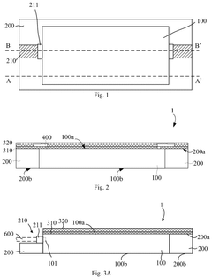
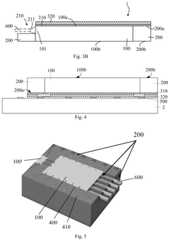
Silicon photonic chip package module based on plastic encapsulation
PatentPendingUS20250291137A1
Innovation
- The proposed silicon photonic chip package module includes a transparent cushioning material layer covering the port of the silicon photonic chip, a plastic encapsulation layer with grooves for fiber optics, and a metal interconnect layer replacing conventional metal wires, allowing direct optical connection to a fiber optic and reducing alignment errors.
Thermal Management Considerations
Thermal management represents one of the most critical challenges in silicon photonics interconnect module packaging. As integration densities increase and data rates push beyond 100 Gbps per channel, thermal considerations have become a limiting factor in system performance and reliability. Silicon photonics devices exhibit significant temperature sensitivity, with wavelength shifts of approximately 0.1 nm/°C in resonant structures and performance degradation when operating outside optimal temperature ranges.
The thermal challenges stem from multiple heat sources within these modules. Active components such as lasers, modulators, and drivers generate substantial heat during operation, with laser diodes typically dissipating 0.5-2W depending on their configuration. Additionally, the thermal conductivity mismatch between materials (silicon at 149 W/m·K versus polymer underfills at 0.2-0.3 W/m·K) creates thermal bottlenecks that impede efficient heat dissipation.
Current thermal management approaches employ multi-tiered strategies. Passive cooling techniques include optimized heat spreaders, typically copper or diamond-like carbon materials with thermal conductivities exceeding 1000 W/m·K. These spreaders are strategically positioned to create efficient thermal pathways from heat-generating components to the package exterior. Thermal interface materials (TIMs) with conductivities ranging from 3-10 W/m·K are utilized to minimize contact resistance between different package elements.
Active cooling solutions incorporate thermoelectric coolers (TECs) for precise temperature control of temperature-sensitive components, particularly lasers. These TECs maintain optimal operating temperatures within ±0.1°C but introduce additional power consumption of 1-3W. Micro-fluidic cooling channels represent an emerging approach, offering cooling capacities exceeding 500 W/cm² in laboratory demonstrations, though commercial implementation remains limited due to reliability concerns.
Thermal simulation and modeling have become essential in the design process. Finite element analysis tools enable accurate prediction of thermal gradients and hotspots before physical prototyping. Advanced packages now incorporate distributed temperature sensors to enable real-time thermal monitoring and adaptive management strategies, maintaining optimal performance across varying workloads and environmental conditions.
Future thermal management innovations focus on heterogeneous integration of cooling elements directly into the silicon interposer layer. Research indicates that embedded micro-channel cooling could potentially handle heat fluxes exceeding 1000 W/cm². Additionally, phase-change materials with high latent heat capacity are being explored to buffer thermal transients during burst-mode operations, potentially reducing peak temperatures by 15-20°C during high-intensity data transmission periods.
Manufacturing Scalability Assessment
The scalability of manufacturing processes for silicon photonics interconnect modules presents significant challenges that must be addressed to enable widespread commercial adoption. Current manufacturing approaches often rely on customized processes that are difficult to scale efficiently, resulting in higher costs and limited production capacity. The transition from laboratory-scale fabrication to high-volume manufacturing requires substantial process optimization and standardization.
One critical factor affecting manufacturing scalability is the alignment precision required between optical components. Silicon photonics interconnects typically demand sub-micron alignment accuracy, which necessitates specialized equipment and processes that are inherently more difficult to scale than traditional electronics manufacturing. Automated assembly systems with machine vision and active alignment capabilities are being developed, but their throughput remains significantly lower than electronic packaging processes.
Material compatibility issues further complicate manufacturing scalability. The integration of different materials with varying thermal expansion coefficients creates challenges in maintaining optical alignment during temperature fluctuations. This necessitates careful material selection and specialized bonding techniques that may not be readily adaptable to high-volume production environments.
Test and verification processes represent another bottleneck in scaling manufacturing. Unlike electronic components that can be tested using standardized electrical probes, optical interconnects require specialized optical test equipment and procedures. The development of wafer-level testing capabilities for optical functionality remains limited, forcing manufacturers to rely on more time-consuming module-level testing approaches.
Supply chain maturity also impacts manufacturing scalability. The ecosystem for silicon photonics components remains fragmented, with limited standardization across suppliers. This results in variability between components and necessitates additional qualification steps that impede scaling efforts. The establishment of industry standards for key components would significantly enhance manufacturing scalability.
Cost structures present additional challenges, as current manufacturing approaches involve numerous specialized processes that do not benefit from the economies of scale seen in mature semiconductor manufacturing. The capital investment required for dedicated equipment further increases the barrier to achieving cost-effective high-volume production. Innovations in process simplification and equipment sharing across product lines are needed to improve cost structures.
Recent industry initiatives are focusing on developing more scalable manufacturing approaches, including the adoption of semiconductor-style automation and process control methodologies. These efforts aim to increase throughput while maintaining the precision required for optical functionality, potentially enabling the production volumes necessary for broader market adoption of silicon photonics interconnect technologies.
Unlock deeper insights with PatSnap Eureka Quick Research — get a full tech report to explore trends and direct your research. Try now!
Generate Your Research Report Instantly with AI Agent
Supercharge your innovation with PatSnap Eureka AI Agent Platform!