

How MWCNT Inks Maintain Conductive Pathways On Flexible Substrates?
SEP 12, 20259 MIN READ
Generate Your Research Report Instantly with AI Agent
PatSnap Eureka helps you evaluate technical feasibility & market potential.
MWCNT Conductive Ink Technology Background and Objectives
Multi-walled carbon nanotubes (MWCNTs) have emerged as a revolutionary material in the field of flexible electronics since their discovery in 1991. These cylindrical nanostructures, consisting of multiple layers of graphene sheets rolled into concentric tubes, possess exceptional electrical conductivity, mechanical strength, and thermal stability. The evolution of MWCNT technology has progressed from laboratory curiosities to commercially viable materials for various applications, particularly in the realm of conductive inks for flexible substrates.
The development of MWCNT conductive inks represents a significant advancement in printed electronics technology. Initially, carbon-based conductive materials were limited to carbon black and graphite, which offered modest conductivity. The introduction of carbon nanotubes in the early 2000s marked a paradigm shift, providing substantially higher conductivity while maintaining flexibility. By the 2010s, researchers had overcome many of the early challenges related to MWCNT dispersion and ink formulation, leading to more stable and printable compositions.
The technical trajectory of MWCNT inks has been characterized by continuous improvements in dispersion techniques, functionalization methods, and ink formulation strategies. Early formulations struggled with nanotube aggregation and poor adhesion to substrates, limiting their practical applications. Recent advancements have focused on enhancing the stability of MWCNT dispersions through surface modifications and the development of novel surfactants and polymeric dispersants.
The primary objective of MWCNT conductive ink technology is to create stable, highly conductive pathways on flexible substrates that maintain their electrical properties under mechanical stress. This involves addressing several key challenges: achieving uniform dispersion of MWCNTs in suitable vehicles, ensuring strong adhesion to various substrate materials, and maintaining conductivity during bending, folding, and stretching operations.
Current research trends are moving toward hybrid systems that combine MWCNTs with other conductive materials such as silver nanoparticles or graphene to enhance performance. Additionally, there is growing interest in environmentally friendly formulations that reduce or eliminate toxic solvents while maintaining processability and performance.
The global push toward flexible, wearable, and stretchable electronics has accelerated the development of MWCNT conductive ink technology. Applications range from flexible displays and solar cells to wearable health monitors and smart textiles. The market demand for these applications is projected to grow exponentially in the coming decade, driving further innovation in MWCNT ink formulations.
Technical goals for the near future include achieving conductivity values approaching those of metallic inks while maintaining superior flexibility, developing low-temperature curing processes compatible with heat-sensitive substrates, and creating formulations suitable for high-resolution printing techniques such as inkjet and aerosol printing.
Market Analysis for Flexible Electronics Applications
The flexible electronics market has experienced remarkable growth in recent years, with a projected market value exceeding $40 billion by 2027, growing at a CAGR of approximately 15%. This surge is primarily driven by increasing demand for wearable devices, foldable displays, and flexible sensors across various industries including healthcare, consumer electronics, and automotive sectors.
Multi-walled carbon nanotube (MWCNT) inks represent a significant segment within this market, particularly valued for their ability to maintain conductive pathways on flexible substrates even under mechanical stress. The market for conductive inks specifically for flexible electronics applications is estimated to reach $3.5 billion by 2025, with carbon-based conductive materials accounting for approximately 25% of this market share.
Consumer electronics remains the largest application segment, constituting nearly 40% of the total flexible electronics market. Within this segment, smartphones with flexible displays and wearable fitness trackers represent the most substantial revenue generators. The healthcare sector follows closely, with a growing demand for flexible biosensors and medical monitoring devices that utilize MWCNT-based conductive pathways.
Regional analysis indicates that Asia-Pacific dominates the flexible electronics market, accounting for over 45% of global production, with South Korea, Japan, and China leading manufacturing capabilities. North America and Europe follow with significant research initiatives and specialized applications in medical and aerospace sectors.
Market trends reveal increasing consumer preference for lightweight, durable, and conformable electronic products. This has accelerated demand for MWCNT inks that can maintain conductivity under repeated bending, stretching, and folding conditions. Industry surveys indicate that consumers are willing to pay a premium of 15-20% for electronic devices with flexible features compared to rigid alternatives.
The competitive landscape shows that companies investing in MWCNT ink technologies for flexible substrates are experiencing above-average growth rates. Strategic partnerships between ink manufacturers and device producers have increased by 30% in the past three years, indicating a collaborative approach to market development.
Market challenges include price sensitivity, with MWCNT inks currently commanding a price premium of 30-40% over traditional silver-based conductive inks. However, as manufacturing scales increase and processing techniques improve, this price differential is expected to narrow to 15-20% by 2025, potentially accelerating market adoption across more price-sensitive application segments.
Current Challenges in MWCNT Ink Conductivity on Flexible Substrates
Despite significant advancements in multi-walled carbon nanotube (MWCNT) ink technology, several critical challenges persist in maintaining consistent conductivity on flexible substrates. The primary obstacle remains the mechanical stability of conductive pathways during substrate deformation. When flexible substrates undergo bending, stretching, or twisting, the MWCNT networks experience significant strain that can disrupt the conductive pathways, leading to performance degradation or complete failure.
The dispersion quality of MWCNTs within the ink formulation presents another substantial challenge. Carbon nanotubes naturally tend to agglomerate due to strong van der Waals forces, forming bundles that create non-uniform distribution across the substrate. These agglomerations result in inconsistent electrical properties and potential weak points in the conductive network that are particularly vulnerable during substrate flexing.
Adhesion between the MWCNT ink and various flexible substrate materials continues to be problematic. Poor adhesion leads to delamination during repeated flexing cycles, completely disrupting the conductive pathway. The interface chemistry between the ink components and substrate surfaces varies widely across different materials, necessitating customized formulations for specific applications.
Environmental stability represents another significant hurdle. MWCNT-based conductive pathways on flexible substrates often demonstrate sensitivity to humidity, temperature fluctuations, and oxidation. These environmental factors can progressively degrade conductivity through mechanisms such as oxidative damage to the nanotubes or moisture-induced swelling of binder materials that disrupt the conductive network.
Manufacturing scalability challenges further complicate widespread adoption. Current deposition techniques struggle to maintain uniform MWCNT orientation and density across large substrate areas. Variations in coating thickness and nanotube alignment create inconsistent electrical properties that become more pronounced during substrate deformation.
The trade-off between conductivity and flexibility remains a fundamental challenge. Increasing MWCNT concentration improves conductivity but typically reduces flexibility and increases brittleness. Conversely, formulations optimized for flexibility often sacrifice conductivity performance. Finding the optimal balance for specific application requirements continues to challenge researchers and manufacturers.
Contact resistance between individual MWCNTs within the network significantly impacts overall conductivity. This resistance increases during substrate deformation as nanotubes shift position relative to each other, temporarily or permanently disrupting junction points. Current research efforts focus on developing novel additives and processing techniques to maintain stable inter-tube connections during dynamic mechanical stress.
Current Approaches to Maintaining MWCNT Conductive Pathways
01 Formulation of MWCNT-based conductive inks
Multi-walled carbon nanotube (MWCNT) inks can be formulated with specific solvents, dispersants, and additives to create stable suspensions suitable for printing applications. These formulations typically include surfactants to prevent agglomeration and binders to enhance adhesion to substrates. The viscosity and surface tension of the ink are carefully controlled to ensure compatibility with various printing techniques such as inkjet, screen printing, or direct writing methods.- MWCNT ink formulations for conductive pathways: Multi-walled carbon nanotube (MWCNT) inks can be formulated with specific dispersants, solvents, and additives to create stable suspensions suitable for printing conductive pathways. These formulations typically include functionalized MWCNTs to improve dispersion stability and prevent agglomeration. The ink composition can be optimized for viscosity, surface tension, and drying characteristics to ensure compatibility with various printing methods such as inkjet, screen printing, or direct writing techniques.
- Printing techniques for MWCNT conductive pathways: Various printing techniques can be employed to deposit MWCNT inks for creating conductive pathways. These include inkjet printing for high-precision patterns, screen printing for thicker films, direct writing for customized geometries, and aerosol jet printing for fine features. Each technique requires specific ink rheological properties and processing parameters to achieve optimal conductivity and adhesion to the substrate. Post-processing treatments such as thermal annealing or laser sintering can further enhance the conductivity of the printed pathways.
- Substrate integration and interface engineering: The integration of MWCNT conductive pathways with various substrates requires careful interface engineering to ensure good adhesion and electrical contact. Surface treatments and functionalization of both the substrate and the MWCNTs can improve wetting and bonding. Flexible, stretchable, and rigid substrates each present unique challenges for MWCNT ink deposition and require tailored approaches to maintain conductivity under mechanical stress or environmental conditions. Compatibility with existing electronic components and interconnection technologies is also essential for practical applications.
- Enhancement of electrical conductivity in MWCNT pathways: Various methods can be employed to enhance the electrical conductivity of MWCNT-based conductive pathways. These include the addition of metallic nanoparticles (such as silver or gold) to create hybrid conductive networks, chemical doping to modify the electronic properties of the MWCNTs, and post-deposition treatments like thermal annealing or compression to improve contact between individual nanotubes. The alignment of MWCNTs during the deposition process can also significantly improve directional conductivity in the printed pathways.
- Applications of MWCNT conductive pathways: MWCNT-based conductive pathways find applications in various fields including flexible electronics, wearable devices, sensors, electromagnetic shielding, and energy storage systems. Their unique combination of electrical conductivity, mechanical flexibility, and thermal stability makes them suitable for next-generation electronic devices. Specific applications include transparent conductive films for touch screens, printed circuit boards, radio frequency identification (RFID) antennas, strain sensors, and interconnects for integrated circuits. The scalability of printing processes also enables mass production of MWCNT-based electronic components.
02 Printing techniques for MWCNT conductive pathways
Various printing methods can be employed to create conductive pathways using MWCNT inks. These include inkjet printing for high-precision patterns, screen printing for thicker films, direct writing for customized geometries, and aerosol jet printing for fine features. Each technique offers different advantages in terms of resolution, throughput, and compatibility with substrate materials. The printing parameters such as nozzle size, printing speed, and substrate temperature significantly influence the conductivity and mechanical properties of the resulting pathways.Expand Specific Solutions03 Post-processing treatments to enhance conductivity
After printing MWCNT inks, various post-processing treatments can be applied to enhance the electrical conductivity of the pathways. These include thermal annealing to remove solvents and improve contact between nanotubes, laser sintering for localized heating without damaging temperature-sensitive substrates, and chemical treatments to remove surfactants that may impede electron transport. Some approaches also incorporate compression or calendering to increase the density of the nanotube network and reduce junction resistance.Expand Specific Solutions04 Substrate compatibility and adhesion mechanisms
MWCNT inks can be formulated to adhere to various substrates including flexible polymers, paper, textiles, and rigid materials like glass or ceramics. The adhesion mechanisms involve physical interlocking, chemical bonding, or a combination of both. Surface treatments such as plasma activation or chemical functionalization can be applied to the substrate to improve wetting and adhesion. For flexible applications, the ink formulation must maintain conductivity under bending, stretching, or folding conditions.Expand Specific Solutions05 Applications and performance characteristics
MWCNT ink-based conductive pathways find applications in flexible electronics, wearable devices, sensors, electromagnetic shielding, and energy storage systems. The performance characteristics of these pathways include electrical conductivity typically ranging from 10² to 10⁵ S/m, mechanical flexibility with minimal change in resistance after thousands of bending cycles, and environmental stability against humidity and temperature variations. The thickness of the printed layers, typically between 1-50 μm, affects both the conductivity and flexibility of the pathways.Expand Specific Solutions
Leading Manufacturers and Research Institutions in MWCNT Ink Development
The MWCNT (Multi-Walled Carbon Nanotube) ink market for flexible electronics is currently in a growth phase, with an estimated market size of $450-500 million and projected CAGR of 15-20% through 2028. The technology has reached moderate maturity, with companies like CHASM Advanced Materials, Brewer Science, and Global Graphene Group leading commercial applications through proprietary formulations that maintain conductivity during substrate deformation. Academic institutions including MIT, Rice University, and Georgia Tech are advancing fundamental research on nanotube dispersion and interface engineering. Meanwhile, industrial players such as Samsung Electronics and Haydale Graphene Industries are focusing on scalable manufacturing processes and integration with existing electronics production. The competitive landscape shows a balance between specialized materials companies and larger electronics manufacturers seeking to incorporate this technology into flexible displays, sensors, and wearable devices.
CHASM Advanced Materials, Inc.
Technical Solution: CHASM Advanced Materials has developed proprietary AgeNT™ transparent conductive films using MWCNT (Multi-Walled Carbon Nanotube) inks specifically designed for flexible substrates. Their technology combines silver nanowires with carbon nanotubes to create hybrid structures that maintain conductivity during bending and flexing. The company's MWCNT formulations include specialized dispersants and rheology modifiers that prevent nanotube aggregation during the drying process, ensuring uniform conductive pathways. CHASM's manufacturing process involves precise control of MWCNT aspect ratios (typically 1000:1) and concentrations (0.1-1.0 wt%) to optimize percolation thresholds while maintaining ink printability[1]. Their inks achieve sheet resistances below 100 Ω/sq with over 85% optical transparency and can withstand over 100,000 bending cycles at a 5mm radius without significant conductivity loss[2].
Strengths: Superior flexibility retention compared to ITO coatings; hybrid silver-CNT approach provides redundant conductive pathways; excellent optical transparency with good conductivity. Weaknesses: Higher sheet resistance than pure metal films; requires specialized printing equipment for optimal deposition; potential for nanotube migration over extended use periods.
Brewer Science, Inc.
Technical Solution: Brewer Science has pioneered MWCNT ink formulations specifically engineered for maintaining conductivity on flexible substrates through their Carbon Electronics Platform. Their approach focuses on chemical functionalization of MWCNTs to enhance dispersion stability and substrate adhesion. The company's proprietary process involves acid treatment of nanotubes to create carboxyl groups, followed by attachment of custom-designed polymer dispersants that provide both steric and electrostatic stabilization. This prevents MWCNT aggregation during flexing events. Their inks contain 1-3% MWCNT content with viscosities carefully controlled between 10-50 cP for compatibility with various printing methods[3]. Brewer's formulations incorporate elastomeric binders that form mechanical bridges between nanotubes, allowing the conductive network to stretch without breaking electrical connections. Testing shows their MWCNT films maintain over 90% of original conductivity after 10,000 bending cycles at 3mm radius, with sheet resistances typically in the 200-500 Ω/sq range depending on film thickness[4].
Strengths: Exceptional adhesion to various polymer substrates; formulations compatible with standard printing equipment; excellent bend fatigue resistance; minimal hysteresis in resistance during repeated flexing. Weaknesses: Higher sheet resistance compared to metal-based conductors; requires careful control of drying conditions to prevent coffee ring effects; limited maximum current capacity compared to metal traces.
Key Patents and Research on MWCNT Ink-Substrate Adhesion
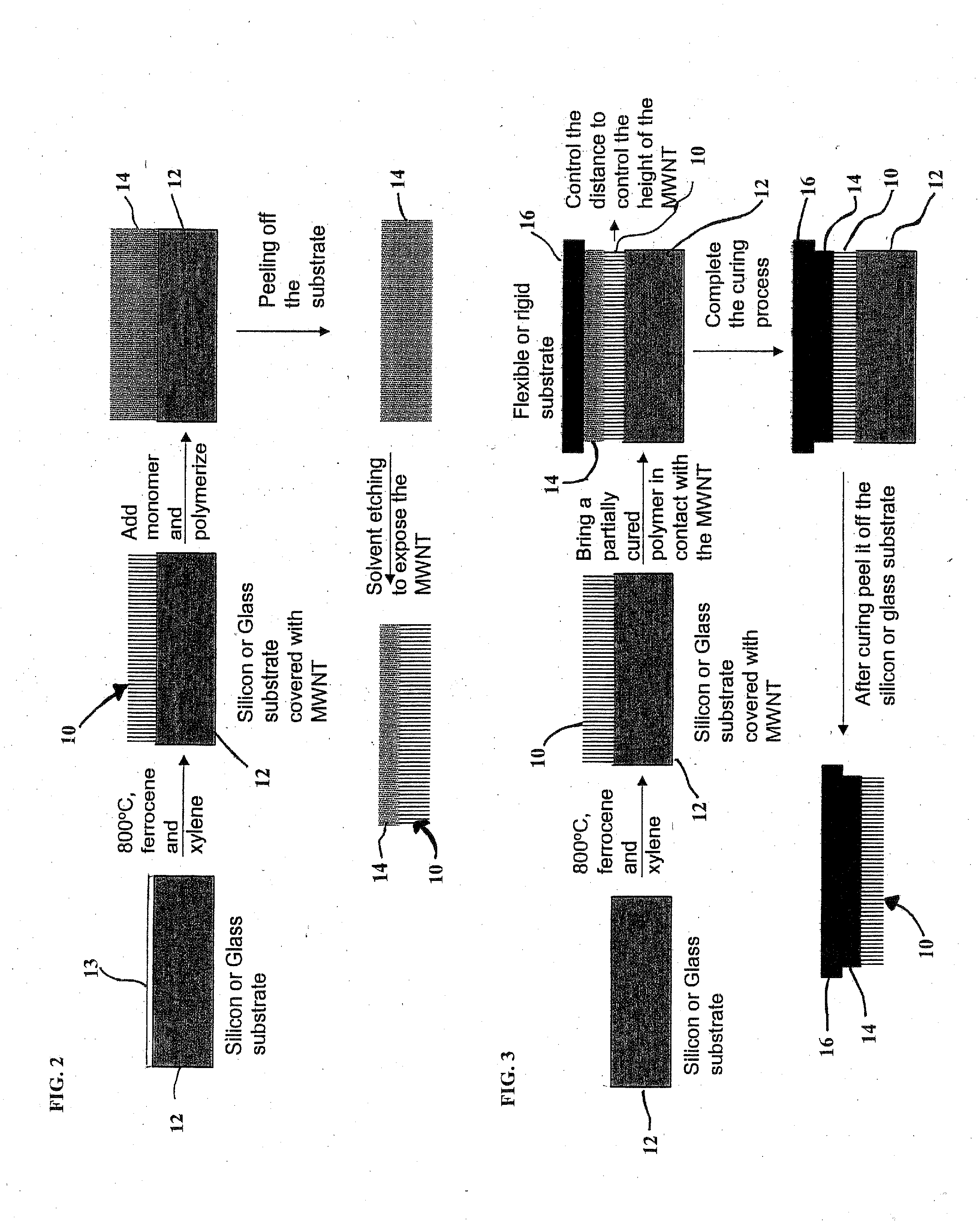
Aligned Carbon Nanotube-Polymer Materials, Systems and Methods
PatentActiveUS20100075024A1
Innovation
- Carbon nanostructure composite systems are formed by embedding organized nanotubes into a polymer matrix, creating a flexible skin-like material with controlled nanotube architecture, orientation, and spacing, achieving strong adhesion and conductivity, similar to gecko foot-hairs, for use in various applications including dry adhesives and electronic systems.

Multilayer carbon nanotube assembly, multilayer carbon nanotube dispersion liquid, conductive material, electrode, secondary battery, planar assembly, filter, electromagnetic wave shield, and pellicle for extreme ultraviolet rays
PatentWO2025013504A1
Innovation
- A multi-walled carbon nanotube aggregate with a length of 1000 μm to 30000 μm and a Fe atom content ratio of 0.5% to 10% by mass, formed into sheet-like or fibrous structures, is developed to enhance conductivity and dispersibility, using methods like chemical vapor deposition and specific processing techniques to control the entanglement and distribution of Fe atoms.


Environmental Impact and Sustainability of MWCNT Ink Production
The production and application of MWCNT (Multi-Walled Carbon Nanotube) inks for flexible electronics present significant environmental considerations that must be addressed as this technology advances toward widespread commercial adoption. The manufacturing processes for carbon nanotubes typically involve energy-intensive methods such as chemical vapor deposition, arc discharge, or laser ablation, resulting in substantial carbon footprints that contradict the sustainable technology narrative.
Raw material extraction for MWCNT production, particularly metal catalysts like nickel, cobalt, and iron, involves mining operations with considerable environmental impacts including habitat destruction, soil contamination, and water pollution. Additionally, the purification and functionalization of MWCNTs often require harsh chemicals and solvents that may pose environmental hazards if not properly managed.
The formulation of MWCNT inks introduces further sustainability challenges. Traditional ink vehicles frequently incorporate volatile organic compounds (VOCs) and toxic solvents that contribute to air pollution and pose health risks to workers. Recent research has focused on developing water-based MWCNT ink formulations that significantly reduce these environmental concerns while maintaining electrical performance on flexible substrates.
Waste management represents another critical environmental dimension. Nanomaterial waste requires specialized handling procedures to prevent environmental contamination, as MWCNTs may persist in ecosystems with potential bioaccumulation effects. Advanced filtration systems and closed-loop manufacturing processes are being implemented to capture and recycle nanomaterial waste, reducing environmental discharge.
Life cycle assessment (LCA) studies of MWCNT-based flexible electronics reveal both challenges and opportunities. While production phases carry substantial environmental burdens, the extended lifespan of MWCNT-enhanced products and their potential contribution to energy-efficient technologies may offset initial impacts. Furthermore, the durability of conductive pathways on flexible substrates reduces replacement frequency, potentially decreasing overall material consumption.
Industry leaders are increasingly adopting green chemistry principles in MWCNT ink development, focusing on reduced toxicity, energy efficiency, and renewable feedstocks. Biomass-derived carbon sources and environmentally benign solvents represent promising directions for sustainable MWCNT ink production while maintaining electrical performance under mechanical stress on flexible substrates.
Regulatory frameworks worldwide are evolving to address nanomaterial environmental impacts, with organizations like the EPA and EU implementing specific guidelines for nanomaterial handling and disposal. Compliance with these regulations drives innovation toward more sustainable production methods that preserve the conductive integrity of MWCNT networks on flexible substrates while minimizing environmental footprint.
Scalability and Manufacturing Process Optimization
The scalability of MWCNT ink technology represents a critical factor in its commercial viability for flexible electronics applications. Current manufacturing processes demonstrate varying degrees of efficiency, with roll-to-roll printing emerging as the most promising approach for high-volume production. This method enables continuous deposition of MWCNT inks onto flexible substrates at speeds reaching 10-30 meters per minute, significantly outpacing traditional batch processing techniques.
Process optimization efforts have focused on several key parameters that directly impact the maintenance of conductive pathways. Ink rheology modification through viscosity control (typically maintained between 10-50 cP) ensures optimal flow characteristics during deposition while preventing nozzle clogging in inkjet systems. Additionally, surface tension adjustment (28-35 mN/m) promotes proper substrate wetting without excessive spreading that could disrupt conductive network formation.
Post-deposition processing has undergone substantial refinement, with curing temperature reduction representing a major advancement. Earlier processes required temperatures exceeding 200°C, limiting substrate compatibility. Recent innovations have enabled effective curing at 120-150°C, expanding the range of usable flexible materials including PET and certain polyimides. Flash photonic sintering has further reduced thermal requirements, using millisecond light pulses to achieve conductivity without substrate damage.
Scalable quality control systems have been integrated into production lines, employing real-time electrical resistance monitoring and optical inspection to ensure consistent conductive pathway formation. These systems can detect defects as small as 10 μm, enabling immediate process adjustments to maintain product specifications across large production volumes.
Material efficiency has improved substantially, with advanced deposition techniques reducing MWCNT waste by 30-40% compared to early manufacturing methods. Closed-loop solvent recovery systems now recapture up to 85% of volatile components, addressing both environmental concerns and production costs. These improvements have contributed to a 45% reduction in per-unit manufacturing costs over the past five years.
The integration of these optimized processes into existing electronics manufacturing infrastructure presents ongoing challenges. Current compatibility issues with standard SMT (Surface Mount Technology) equipment require either specialized handling systems or adaptation of existing production lines. Industry leaders are developing standardized interfaces to facilitate seamless integration, potentially accelerating widespread adoption across multiple electronics manufacturing sectors.
Unlock deeper insights with PatSnap Eureka Quick Research — get a full tech report to explore trends and direct your research. Try now!
Generate Your Research Report Instantly with AI Agent
Supercharge your innovation with PatSnap Eureka AI Agent Platform!