

How to Boost Semiconductor Photodetector Responsivity
MAR 31, 20269 MIN READ
Generate Your Research Report Instantly with AI Agent
PatSnap Eureka helps you evaluate technical feasibility & market potential.
Semiconductor Photodetector Development Background and Goals
Semiconductor photodetectors have emerged as critical components in modern optoelectronic systems, with their development spanning over six decades since the first silicon photodiodes were demonstrated in the 1950s. The evolution from simple p-n junction devices to sophisticated avalanche photodiodes, PIN photodiodes, and quantum dot detectors reflects the continuous pursuit of enhanced performance metrics, particularly responsivity enhancement.
The historical trajectory of photodetector development reveals distinct phases of technological advancement. Early germanium and silicon-based devices established fundamental principles, while the introduction of III-V compound semiconductors in the 1970s expanded spectral coverage into infrared regions. The subsequent development of heterostructure devices and quantum-confined structures has pushed the boundaries of detection sensitivity and speed.
Current technological trends indicate a strong emphasis on material engineering approaches to boost responsivity. The integration of novel materials such as graphene, transition metal dichalcogenides, and perovskites represents a paradigm shift toward hybrid photodetector architectures. Additionally, the emergence of plasmonic enhancement techniques and metamaterial-based structures demonstrates the industry's commitment to overcoming traditional responsivity limitations.
The primary technical objectives driving contemporary photodetector research center on achieving responsivity values exceeding conventional theoretical limits while maintaining acceptable noise characteristics and response times. Specific targets include developing devices capable of single-photon detection across extended spectral ranges, implementing gain mechanisms that preserve signal integrity, and creating cost-effective manufacturing processes for high-performance devices.
Strategic goals encompass the realization of photodetectors with responsivity enhancement factors of 10-100x compared to conventional devices, particularly for applications in quantum communication, medical imaging, and autonomous vehicle systems. The integration of artificial intelligence-driven optimization techniques for device design represents an emerging objective, enabling the systematic exploration of complex parameter spaces to identify optimal responsivity enhancement strategies.
Future development trajectories focus on multidisciplinary approaches combining advanced materials science, nanofabrication techniques, and novel device architectures. The convergence of these technological streams aims to establish new benchmarks for photodetector performance while addressing scalability and commercial viability requirements essential for widespread adoption across diverse application domains.
Market Demand for High-Responsivity Photodetectors
The global semiconductor photodetector market is experiencing unprecedented growth driven by the convergence of multiple technological revolutions. Telecommunications infrastructure demands increasingly sensitive photodetectors to support high-speed fiber optic networks and emerging 5G applications. The proliferation of data centers and cloud computing services requires photodetectors capable of handling massive data throughput with minimal signal loss, making responsivity a critical performance parameter.
Autonomous vehicle development has created substantial demand for high-performance LiDAR systems, where photodetector responsivity directly impacts detection range and accuracy. Advanced driver assistance systems rely on photodetectors to process real-time environmental data, necessitating devices with enhanced sensitivity across various wavelengths. The automotive sector's transition toward fully autonomous vehicles continues to expand market opportunities for high-responsivity photodetectors.
Medical and healthcare applications represent another significant growth driver. Optical coherence tomography, fluorescence imaging, and non-invasive diagnostic equipment require photodetectors with exceptional sensitivity to detect weak optical signals. The aging global population and increased healthcare spending fuel demand for advanced medical imaging systems incorporating high-responsivity photodetectors.
Industrial automation and manufacturing sectors increasingly adopt machine vision systems for quality control and process monitoring. These applications demand photodetectors capable of detecting subtle variations in optical signals under challenging environmental conditions. Smart manufacturing initiatives and Industry 4.0 implementations further accelerate adoption of advanced photodetection technologies.
Consumer electronics markets drive volume demand for photodetectors in smartphones, tablets, and wearable devices. Ambient light sensors, proximity detectors, and biometric authentication systems require compact, energy-efficient photodetectors with enhanced responsivity. The Internet of Things expansion creates additional opportunities for photodetector integration in smart home devices and environmental monitoring systems.
Scientific research and defense applications maintain steady demand for cutting-edge photodetector technologies. Spectroscopy, astronomy, and quantum research require photodetectors with ultimate sensitivity and low noise characteristics. Military and aerospace applications demand ruggedized photodetectors capable of operating under extreme conditions while maintaining high responsivity performance.
The market exhibits strong regional variations, with Asia-Pacific leading in manufacturing volume while North America and Europe focus on high-value applications. Emerging markets show increasing adoption of photodetector-enabled technologies, creating new growth opportunities for manufacturers developing cost-effective, high-responsivity solutions.
Current Responsivity Limitations and Technical Challenges
Semiconductor photodetectors face several fundamental limitations that constrain their responsivity performance across different wavelength ranges and application scenarios. The most significant challenge stems from the inherent trade-off between quantum efficiency and carrier collection efficiency. While increasing the active layer thickness can enhance photon absorption, it simultaneously reduces the electric field strength and increases carrier transit time, leading to higher recombination losses and reduced bandwidth performance.
Material-related constraints represent another critical bottleneck in responsivity enhancement. The bandgap characteristics of conventional semiconductor materials limit their spectral response range, particularly in infrared applications where longer wavelengths require narrower bandgap materials. These materials often suffer from higher dark current levels and increased thermal noise, which directly impact the signal-to-noise ratio and overall detector performance.
Surface recombination losses constitute a major technical challenge, especially in devices with high surface-to-volume ratios. Dangling bonds and defect states at semiconductor surfaces create non-radiative recombination centers that significantly reduce the effective quantum efficiency. This issue becomes more pronounced in advanced device architectures such as nanowire arrays or quantum dot structures, where surface effects dominate the carrier dynamics.
Carrier transport limitations present additional obstacles to achieving high responsivity. In many semiconductor photodetectors, the minority carrier diffusion length is shorter than the optical absorption length, resulting in incomplete carrier collection. This mismatch is particularly problematic in materials with high defect densities or poor crystal quality, where carrier lifetimes are severely compromised.
Optical coupling inefficiencies further limit the achievable responsivity in practical devices. Reflection losses at air-semiconductor interfaces, typically ranging from 30-40% for common semiconductors, represent a significant source of optical loss. Additionally, the mismatch between incident light distribution and the active detector area reduces the effective photon utilization efficiency.
Thermal effects pose substantial challenges for maintaining consistent responsivity performance across different operating conditions. Temperature variations affect both the intrinsic carrier concentration and the bandgap energy, leading to wavelength-dependent responsivity shifts and increased dark current levels that degrade the detector's sensitivity.
Existing Responsivity Boosting Solutions and Approaches
01 Material composition and bandgap engineering for enhanced responsivity
Semiconductor photodetectors can achieve improved responsivity through careful selection and engineering of semiconductor materials with optimized bandgap properties. Different semiconductor materials and their alloys can be utilized to tune the absorption spectrum and quantum efficiency. The use of compound semiconductors and heterostructures allows for better matching with specific wavelength ranges, thereby increasing the photodetector's sensitivity to incident light. Material doping and composition gradients can further enhance carrier collection efficiency and reduce recombination losses.- Material composition and doping optimization for enhanced responsivity: Semiconductor photodetectors can achieve improved responsivity through careful selection and optimization of semiconductor materials and their doping profiles. Different semiconductor materials exhibit varying absorption coefficients and carrier mobility characteristics that directly impact photodetection efficiency. Strategic doping concentration and profile design can enhance the internal electric field distribution, reduce carrier recombination, and improve quantum efficiency. Material engineering approaches include using compound semiconductors, adjusting bandgap properties, and optimizing the active layer thickness to maximize photon absorption while maintaining efficient carrier collection.
- Structural design and geometry optimization: The physical structure and geometric configuration of photodetectors significantly influence their responsivity characteristics. Advanced structural designs include optimized junction depths, surface texturing, and specialized electrode configurations that enhance light coupling and reduce reflection losses. Three-dimensional architectures and novel device geometries can increase the effective absorption path length while maintaining fast carrier transit times. Surface passivation techniques and anti-reflection coatings further improve light absorption efficiency. The integration of optical elements such as microlenses or waveguides can concentrate incident light onto the active detection area, thereby increasing the overall responsivity.
- Heterostructure and quantum engineering approaches: Advanced heterostructure designs and quantum-engineered devices offer enhanced responsivity through sophisticated band engineering. Multiple quantum well structures, superlattices, and type-II heterostructures can be designed to optimize carrier generation and collection efficiency. These structures enable wavelength-selective detection and can extend the spectral response range. Strain engineering in heterostructures modifies the band structure to improve absorption characteristics. The use of graded composition layers and carefully designed barrier heights facilitates efficient carrier extraction while minimizing dark current, resulting in improved signal-to-noise ratios and overall responsivity.
- Avalanche multiplication and gain mechanisms: Incorporating internal gain mechanisms through avalanche multiplication processes can significantly enhance photodetector responsivity. Avalanche photodetectors utilize impact ionization to generate multiple electron-hole pairs from a single absorbed photon, providing internal current gain. Careful design of the multiplication region, including electric field profile optimization and selection of appropriate multiplication layer materials, maximizes gain while controlling noise characteristics. Separate absorption and multiplication regions allow independent optimization of each function. Advanced designs include resonant cavity structures and feedback mechanisms that enhance the effective quantum efficiency beyond unity, dramatically improving responsivity for low-light detection applications.
- Integration with optical and electronic enhancement circuits: System-level integration approaches combine photodetectors with optical concentrators and electronic amplification circuits to boost overall responsivity. Integrated optical elements such as plasmonic structures, photonic crystals, or resonant cavities enhance light-matter interaction within the detector active region. On-chip amplification circuits, including transimpedance amplifiers and low-noise preamplifiers, are co-designed with the photodetector to optimize the overall signal chain performance. Advanced packaging techniques minimize parasitic capacitance and inductance, enabling higher bandwidth operation without sacrificing responsivity. Hybrid integration approaches combine different material systems to leverage the advantages of each technology, achieving superior performance across multiple metrics including responsivity, speed, and spectral range.
02 Structural design and geometry optimization
The physical structure and geometry of photodetectors significantly impact responsivity performance. Various structural configurations including planar, mesa, and waveguide-integrated designs can be employed to maximize light absorption and carrier collection. Anti-reflection coatings and surface texturing techniques help reduce optical losses at interfaces. The optimization of active layer thickness, electrode configuration, and device dimensions enables better light coupling and reduced dark current, contributing to enhanced responsivity across target wavelength ranges.Expand Specific Solutions03 Avalanche multiplication and gain mechanisms
Avalanche photodetectors utilize impact ionization to achieve internal gain, significantly enhancing responsivity beyond unity quantum efficiency. The design of multiplication regions with appropriate electric field profiles enables controlled avalanche breakdown while minimizing excess noise. Separate absorption and multiplication layer structures allow independent optimization of absorption efficiency and gain characteristics. Proper selection of multiplication layer materials and doping profiles ensures high gain-bandwidth products and improved signal-to-noise ratios.Expand Specific Solutions04 Quantum efficiency enhancement through optical structures
Advanced optical structures can be integrated with photodetectors to improve light absorption and quantum efficiency. Resonant cavity designs, distributed Bragg reflectors, and photonic crystal structures enhance light-matter interaction within the active region. Plasmonic nanostructures and metamaterials can be employed to concentrate optical fields and extend absorption paths. These optical enhancement techniques enable higher responsivity without increasing device dimensions or requiring higher bias voltages, particularly beneficial for wavelength-selective detection applications.Expand Specific Solutions05 Novel materials and emerging technologies
Emerging semiconductor materials and novel device architectures offer new pathways for achieving superior photodetector responsivity. Two-dimensional materials, quantum dots, and nanowire structures provide unique optical and electrical properties that can surpass conventional bulk semiconductors. Hybrid organic-inorganic structures and perovskite-based photodetectors demonstrate high absorption coefficients and tunable bandgaps. Advanced fabrication techniques enable the integration of multiple material systems and the creation of complex heterostructures optimized for specific detection requirements across ultraviolet to infrared spectral ranges.Expand Specific Solutions
Key Players in Semiconductor Photodetector Industry
The semiconductor photodetector responsivity enhancement field represents a mature yet rapidly evolving market driven by increasing demand for high-performance optical sensing across telecommunications, automotive, and consumer electronics sectors. The industry is experiencing significant growth with market valuations reaching billions globally, fueled by applications in LiDAR, optical communications, and advanced imaging systems. Technology maturity varies considerably across different approaches, with established players like Hamamatsu Photonics, Sony Semiconductor Solutions, and Mitsubishi Electric leading traditional silicon-based solutions, while innovative companies such as Artilux are pioneering germanium-silicon integrated photonic platforms for enhanced broad-spectrum sensitivity. Research institutions including Fudan University, Southeast University, and the Institute of Microelectronics of Chinese Academy of Sciences are advancing novel materials and device architectures. The competitive landscape shows a mix of mature Japanese corporations, emerging Asian technology companies, and strong academic research contributions, indicating a dynamic ecosystem where both incremental improvements and breakthrough innovations coexist to address diverse application requirements.
Hamamatsu Photonics KK
Technical Solution: Hamamatsu employs advanced avalanche photodiode (APD) technology with optimized multiplication layer structures to achieve high responsivity. Their approach includes using InGaAs/InP heterostructures with carefully engineered electric field profiles to maximize quantum efficiency while minimizing dark current. The company also develops silicon photomultiplier (SiPM) arrays with microcell optimization techniques that enhance photon detection efficiency through improved fill factor and reduced optical crosstalk. Additionally, they implement anti-reflection coatings and surface texturing methods to reduce reflection losses and increase light absorption, resulting in responsivity improvements of up to 30% compared to conventional designs.
Strengths: Industry-leading expertise in photomultiplier technology, excellent signal-to-noise ratio, proven reliability in scientific applications. Weaknesses: Higher cost compared to silicon-based solutions, limited bandwidth in some APD configurations.
Sony Semiconductor Solutions Corp.
Technical Solution: Sony focuses on back-illuminated CMOS image sensor technology with enhanced photodiode structures to boost responsivity. Their approach involves deep trench isolation and optimized pixel architectures that maximize light collection efficiency. The company utilizes copper wiring technology and advanced microlens designs to improve light gathering capabilities. Sony also implements stacked sensor architectures where photodiodes are separated from logic circuits, allowing for larger photodiode areas and improved quantum efficiency. Their proprietary pixel technologies include enhanced spectral response through specialized doping profiles and anti-reflection treatments that can achieve responsivity improvements exceeding 40% in near-infrared applications.
Strengths: Market leadership in CMOS sensors, excellent manufacturing scalability, strong integration capabilities with processing circuits. Weaknesses: Primarily focused on imaging applications, limited expertise in specialized photodetector materials beyond silicon.
Core Patents in Photodetector Responsivity Enhancement
Photodetector with spectrally extended responsivity
PatentInactiveUS6222200B1
Innovation
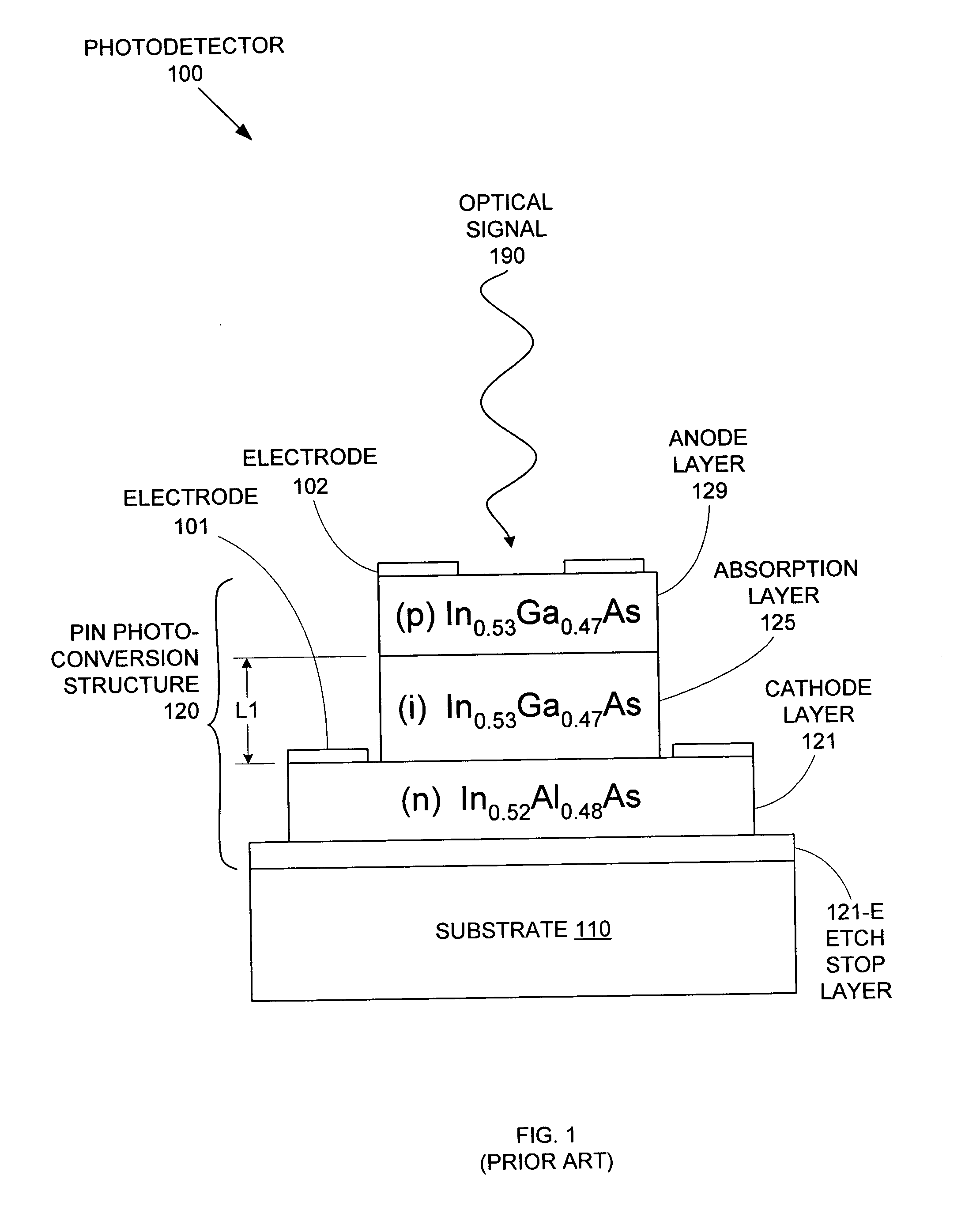
- A photodetector structure with a balanced effective strain in the active region, achieved by optimizing the thickness of alternating compressive and tensile strain layers to prevent crystalline defects and enhance optical absorption, allowing operation from 970 nm to 1800 nm or further.


Increased responsivity photodetector
PatentInactiveUS20050012030A1
Innovation
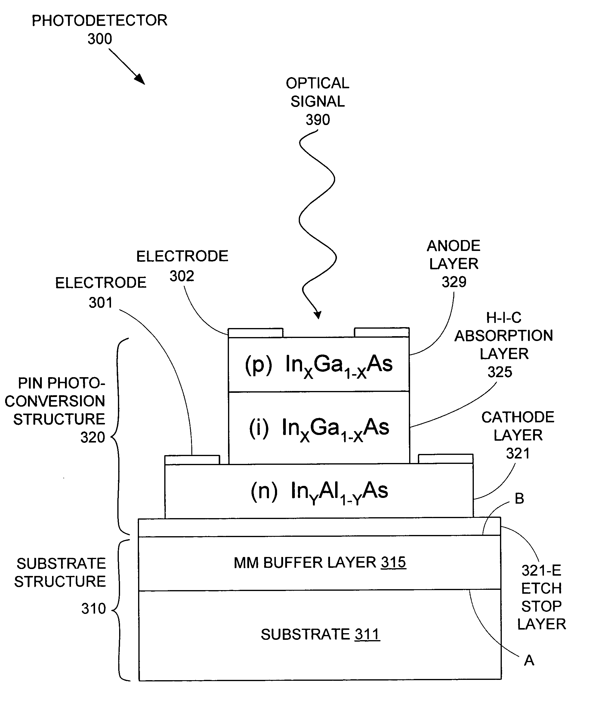
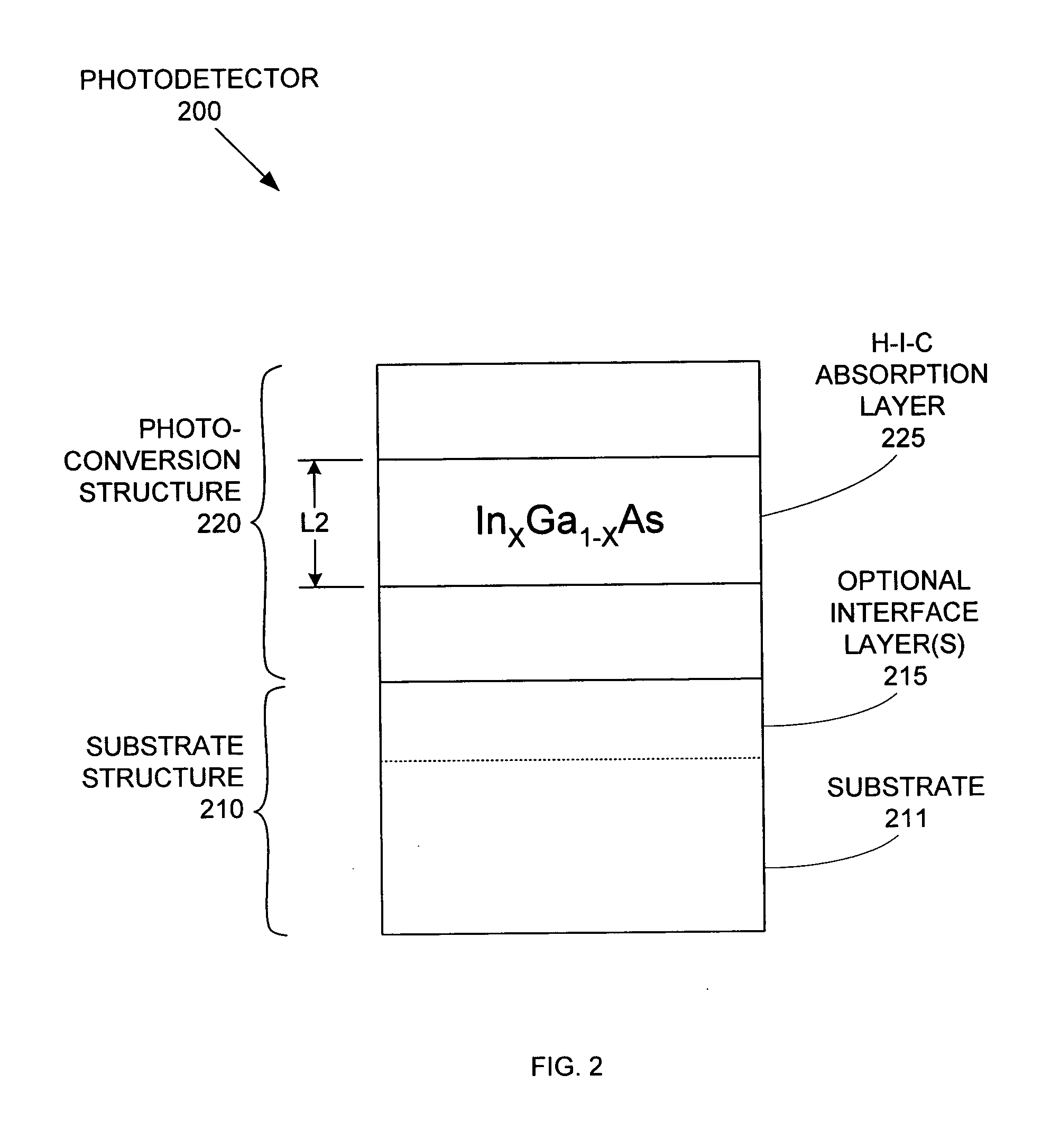
- Increasing the indium concentration in the InGaAs absorption layer beyond 53% to enhance the density of allowable energy states, allowing for higher responsivity without increasing the absorption layer thickness, and using a metamorphic buffer layer to accommodate different lattice constants, enabling the formation of high-indium-concentration photoconversion structures on various substrates.

Material Innovation Strategies for Enhanced Responsivity
Material innovation represents the most fundamental approach to enhancing semiconductor photodetector responsivity, as the intrinsic properties of photoactive materials directly determine the efficiency of photon-to-electron conversion. The strategic development of novel materials and the optimization of existing ones have emerged as critical pathways for achieving breakthrough performance improvements in photodetection applications.
Advanced compound semiconductors offer significant advantages over traditional silicon-based materials in terms of responsivity enhancement. Materials such as indium gallium arsenide (InGaAs), mercury cadmium telluride (HgCdTe), and gallium arsenide phosphide (GaAsP) demonstrate superior absorption coefficients and quantum efficiencies across specific wavelength ranges. These materials enable precise bandgap engineering, allowing for optimized spectral response characteristics tailored to specific application requirements.
Two-dimensional materials have revolutionized the photodetector landscape by providing exceptional surface-to-volume ratios and unique electronic properties. Graphene, transition metal dichalcogenides like molybdenum disulfide (MoS2), and black phosphorus exhibit remarkable photoresponsive characteristics with potential for ultra-high responsivity values. The atomically thin nature of these materials facilitates efficient charge carrier extraction while minimizing recombination losses.
Perovskite materials have gained substantial attention due to their exceptional optoelectronic properties and solution-processable nature. Organic-inorganic hybrid perovskites demonstrate high absorption coefficients, long carrier diffusion lengths, and tunable bandgaps through compositional engineering. These characteristics make them particularly attractive for developing high-responsivity photodetectors with cost-effective manufacturing processes.
Quantum dot integration strategies offer unprecedented control over material properties through size-dependent quantum confinement effects. Colloidal quantum dots, including lead sulfide (PbS), cadmium selenide (CdSe), and indium arsenide (InAs), enable precise spectral tuning and enhanced light absorption. The ability to engineer quantum dot size, shape, and surface chemistry provides multiple pathways for responsivity optimization.
Nanostructured material architectures, including nanowires, nanotubes, and nanocrystals, present unique opportunities for responsivity enhancement through increased surface area and improved light-matter interaction. These structures facilitate efficient photon absorption while providing enhanced charge carrier collection efficiency through reduced transport distances and optimized electric field distributions.
Manufacturing Process Optimization for Responsivity Gains
Manufacturing process optimization represents a critical pathway for achieving substantial responsivity improvements in semiconductor photodetectors through systematic refinement of fabrication techniques. The optimization approach encompasses multiple manufacturing stages, from substrate preparation to final device packaging, with each step offering specific opportunities for performance enhancement.
Epitaxial growth optimization stands as a fundamental manufacturing consideration, where precise control of layer thickness, doping concentrations, and interface quality directly impacts photodetector responsivity. Advanced molecular beam epitaxy and metal-organic chemical vapor deposition techniques enable atomic-level control over semiconductor heterostructures, allowing for optimized absorption layer thickness that maximizes photon capture while minimizing recombination losses. Temperature profiles, growth rates, and precursor flow ratios require careful calibration to achieve optimal crystal quality and minimize defect densities that can degrade quantum efficiency.
Surface passivation processes during manufacturing significantly influence responsivity by reducing surface recombination velocities and improving carrier collection efficiency. Chemical treatments, thermal annealing procedures, and protective layer deposition must be optimized to minimize surface states while maintaining excellent optical transmission properties. The selection of passivation materials and their deposition parameters directly correlates with achieved responsivity levels.
Contact formation and metallization processes require optimization to minimize series resistance and maximize carrier extraction efficiency. Advanced lithography techniques, precise etching parameters, and optimized annealing cycles for ohmic contact formation contribute to improved responsivity by reducing electrical losses. The geometry and placement of electrical contacts must be carefully designed to minimize optical shadowing while ensuring efficient current collection across the active device area.
Antireflection coating optimization during manufacturing provides significant responsivity gains by minimizing optical losses at device interfaces. Multi-layer coating designs with precisely controlled thickness and refractive index profiles can be tailored to specific wavelength ranges, requiring optimization of deposition parameters including temperature, pressure, and material composition ratios.
Process integration optimization focuses on minimizing contamination, controlling thermal budgets, and maintaining consistent processing conditions across manufacturing batches. Statistical process control methodologies enable identification of critical process parameters that most significantly impact responsivity, allowing for targeted optimization efforts that yield maximum performance improvements while maintaining manufacturing yield and cost effectiveness.
Unlock deeper insights with PatSnap Eureka Quick Research — get a full tech report to explore trends and direct your research. Try now!
Generate Your Research Report Instantly with AI Agent
Supercharge your innovation with PatSnap Eureka AI Agent Platform!