How to Implement Eco-Friendly Solutions in EUV Lithography
APR 2, 20269 MIN READ
Generate Your Research Report Instantly with AI Agent
PatSnap Eureka helps you evaluate technical feasibility & market potential.
EUV Lithography Green Technology Background and Objectives
Extreme Ultraviolet (EUV) lithography represents a pivotal advancement in semiconductor manufacturing, enabling the production of chips with feature sizes below 7 nanometers. This technology utilizes light with wavelengths around 13.5 nm to achieve unprecedented precision in pattern transfer onto silicon wafers. However, the implementation of EUV lithography has raised significant environmental concerns due to its substantial energy consumption, complex chemical processes, and resource-intensive infrastructure requirements.
The evolution of EUV lithography began in the 1980s as a research concept and has undergone decades of development to reach commercial viability. Early implementations focused primarily on technical performance metrics such as resolution, throughput, and yield, with limited consideration for environmental impact. The technology's reliance on high-power laser systems, vacuum chambers, and specialized materials has created a substantial carbon footprint that demands immediate attention as the semiconductor industry scales production volumes.
Current environmental challenges in EUV lithography stem from multiple sources including the energy-intensive light source generation process, which requires plasma-based systems consuming significant electrical power. Additionally, the technology demands ultra-pure hydrogen gas for debris mitigation, specialized photoresist materials with complex chemical compositions, and extensive cooling systems to manage thermal loads. These factors collectively contribute to increased greenhouse gas emissions and resource depletion.
The primary objective of implementing eco-friendly solutions in EUV lithography is to achieve a substantial reduction in environmental impact while maintaining or improving manufacturing performance. This encompasses developing energy-efficient light source technologies, implementing sustainable material alternatives, optimizing process parameters to reduce waste generation, and establishing circular economy principles within the manufacturing workflow.
Secondary objectives include minimizing water consumption through advanced recycling systems, reducing hazardous chemical usage by developing environmentally benign alternatives, and implementing smart manufacturing approaches that optimize resource utilization. The ultimate goal is to establish EUV lithography as a sustainable technology platform that supports the semiconductor industry's growth while meeting increasingly stringent environmental regulations and corporate sustainability commitments.
These objectives align with global initiatives toward carbon neutrality and sustainable manufacturing practices, positioning eco-friendly EUV lithography as a critical enabler for the future semiconductor ecosystem.
Market Demand for Sustainable Semiconductor Manufacturing
The semiconductor industry faces unprecedented pressure to adopt sustainable manufacturing practices, driven by increasingly stringent environmental regulations and corporate sustainability commitments. Global semiconductor manufacturers are experiencing mounting demands from regulatory bodies, investors, and customers to reduce their environmental footprint while maintaining production efficiency and quality standards.
Environmental regulations across major semiconductor manufacturing regions have become more restrictive, particularly regarding energy consumption, chemical waste management, and carbon emissions. The European Union's Green Deal and similar initiatives in Asia-Pacific regions are establishing mandatory sustainability benchmarks that directly impact EUV lithography operations. These regulatory frameworks are creating compliance-driven market demand for eco-friendly solutions in advanced semiconductor manufacturing processes.
Corporate sustainability initiatives represent another significant driver of market demand. Leading semiconductor companies have committed to achieving carbon neutrality and implementing circular economy principles in their operations. These commitments translate into substantial investments in sustainable manufacturing technologies, including environmentally conscious EUV lithography solutions. The integration of sustainability metrics into corporate performance indicators has elevated environmental considerations to strategic priority levels.
Supply chain sustainability requirements are reshaping procurement decisions throughout the semiconductor ecosystem. Original equipment manufacturers and foundries are increasingly evaluating suppliers based on environmental performance criteria, creating cascading demand for sustainable technologies across the entire value chain. This trend particularly affects EUV lithography equipment suppliers and chemical manufacturers serving this market segment.
Market research indicates substantial growth potential for sustainable semiconductor manufacturing solutions. The convergence of regulatory compliance requirements, corporate sustainability goals, and operational cost optimization is creating a robust market environment for eco-friendly EUV lithography technologies. Investment patterns show increasing capital allocation toward sustainable manufacturing infrastructure, with particular emphasis on energy-efficient processes and waste reduction technologies.
The competitive landscape is evolving as sustainability becomes a key differentiator in semiconductor manufacturing. Companies demonstrating superior environmental performance are gaining competitive advantages in customer acquisition and retention, while those lagging in sustainability adoption face increasing market pressure and potential regulatory penalties.
Current Environmental Challenges in EUV Lithography Systems
EUV lithography systems face significant environmental challenges that stem from their complex operational requirements and resource-intensive processes. The technology's reliance on extreme ultraviolet light generation creates substantial energy consumption patterns, with typical EUV scanners requiring 200-300 kilowatts of continuous power operation. This high energy demand translates directly into increased carbon footprint and operational costs for semiconductor manufacturing facilities.
Water consumption represents another critical environmental concern in EUV systems. The cooling infrastructure necessary to maintain optimal operating temperatures for laser sources, collector mirrors, and optical components requires substantial water resources. Industrial-scale EUV facilities can consume thousands of gallons of cooling water daily, placing strain on local water resources and generating thermal pollution through heated discharge water.
Chemical waste generation poses complex disposal challenges throughout EUV lithography processes. The photoresist materials, cleaning solvents, and etching chemicals used in conjunction with EUV exposure create hazardous waste streams requiring specialized treatment and disposal protocols. Additionally, the frequent replacement of optical components due to contamination and degradation contributes to electronic waste accumulation.
Atmospheric emissions from EUV systems include both direct and indirect environmental impacts. The hydrogen gas used in plasma generation for EUV light sources, while not directly harmful, requires careful handling and ventilation systems. More concerning are the volatile organic compounds released during photoresist processing and the ozone generation from UV exposure of atmospheric oxygen in inadequately sealed systems.
The manufacturing and maintenance lifecycle of EUV components presents additional environmental burdens. The production of specialized mirrors, masks, and optical elements involves rare earth materials and energy-intensive manufacturing processes. Component replacement frequency, driven by contamination sensitivity and performance degradation, amplifies these environmental impacts through increased material consumption and waste generation.
Facility infrastructure requirements compound environmental challenges through increased building energy consumption for cleanroom maintenance, vibration isolation systems, and electromagnetic shielding. The stringent environmental controls necessary for EUV operation, including ultra-low particle contamination and temperature stability, demand continuous operation of energy-intensive HVAC and filtration systems, further expanding the technology's environmental footprint.
Existing Eco-Friendly Solutions for EUV Systems
01 Water-based photoresist compositions for EUV lithography
Development of environmentally friendly photoresist formulations that utilize water as the primary solvent instead of traditional organic solvents. These compositions reduce volatile organic compound emissions and hazardous waste generation while maintaining high resolution and sensitivity required for extreme ultraviolet lithography processes. The water-based systems incorporate specialized polymers and photoacid generators that are compatible with aqueous environments.- Water-based photoresist compositions for EUV lithography: Development of environmentally friendly photoresist formulations that utilize water as the primary solvent instead of traditional organic solvents. These compositions reduce volatile organic compound emissions and hazardous waste generation while maintaining high resolution and sensitivity required for extreme ultraviolet lithography processes. The water-based systems incorporate specialized polymers and photoacid generators that are compatible with aqueous environments.
- Recyclable and biodegradable resist materials: Implementation of photoresist materials designed for recovery and reuse or safe biodegradation after the lithography process. These materials feature chemical structures that allow for efficient stripping and recycling of components, or incorporate biodegradable polymers that break down into non-toxic substances. This approach significantly reduces chemical waste and environmental impact associated with semiconductor manufacturing.
- Reduced chemical consumption in development and cleaning processes: Optimization of developer solutions and cleaning chemistries to minimize the volume and toxicity of chemicals required for pattern development and substrate cleaning in extreme ultraviolet lithography. These solutions employ more efficient formulations, lower concentration requirements, and alternative chemistries that reduce hazardous waste generation while maintaining process performance and throughput.
- Energy-efficient EUV source and optical systems: Development of extreme ultraviolet light sources and optical components with improved energy conversion efficiency and reduced power consumption. These systems incorporate advanced plasma generation techniques, optimized collector optics, and thermal management solutions that decrease overall energy requirements and associated carbon footprint of the lithography equipment while extending component lifetime.
- Closed-loop chemical recovery and waste treatment systems: Integration of chemical recovery and waste treatment systems that capture, purify, and recycle process chemicals used in extreme ultraviolet lithography operations. These systems employ filtration, distillation, and chemical treatment methods to recover solvents, developers, and other process fluids, significantly reducing fresh chemical consumption and hazardous waste disposal requirements while lowering operational costs.
02 Recyclable and biodegradable resist materials
Implementation of photoresist materials designed for recovery and reuse or safe biodegradation after the lithography process. These materials feature chemical structures that allow for efficient stripping and recycling of components, or incorporate biodegradable polymers that break down into non-toxic substances. This approach significantly reduces chemical waste and environmental impact associated with semiconductor manufacturing.Expand Specific Solutions03 Low-outgassing materials for EUV optics protection
Development of photoresist and coating materials with minimal outgassing properties to prevent contamination of expensive EUV optical components. These materials are formulated to reduce the release of volatile compounds that can deposit on mirrors and degrade system performance, thereby extending equipment lifetime and reducing the need for frequent maintenance and replacement of components.Expand Specific Solutions04 Energy-efficient EUV lithography processing methods
Implementation of processing techniques that reduce energy consumption during exposure, development, and post-processing steps. These methods include optimized baking temperatures, reduced processing times, and efficient use of radiation doses. The approaches minimize the carbon footprint of lithography operations while maintaining pattern quality and throughput requirements.Expand Specific Solutions05 Green solvent systems for resist processing
Utilization of environmentally benign solvents for photoresist coating, development, and cleaning processes. These alternative solvent systems replace hazardous chemicals with safer options such as supercritical carbon dioxide, ionic liquids, or bio-based solvents. The green solvents maintain process compatibility while reducing toxicity, flammability risks, and environmental pollution associated with conventional lithography chemicals.Expand Specific Solutions
Key Players in Sustainable EUV Equipment Industry
The EUV lithography eco-friendly solutions market represents a mature yet rapidly evolving sector within the semiconductor industry, driven by increasing environmental regulations and sustainability demands. The market demonstrates significant scale, with major foundries like TSMC and Samsung Electronics leading adoption alongside equipment manufacturers such as ASML Netherlands BV, which dominates EUV system supply. Technology maturity varies across the ecosystem, with established players like Applied Materials, Lam Research, and Tokyo Electron advancing sustainable manufacturing processes, while materials companies including DuPont Specialty Materials Korea and Shanghai Sinyang Semiconductor Materials develop greener chemical solutions. The competitive landscape shows strong consolidation among tier-one suppliers, with emerging opportunities for specialized environmental technology providers. Companies like Carl Zeiss SMT and NuFlare Technology contribute critical components, while research institutions such as CEA drive innovation in sustainable lithography approaches, indicating a collaborative industry effort toward environmental responsibility.
Taiwan Semiconductor Manufacturing Co., Ltd.
Technical Solution: TSMC has implemented a comprehensive green manufacturing approach for EUV lithography operations, achieving carbon neutrality goals through renewable energy integration and advanced process optimization. Their eco-friendly EUV implementation includes smart grid integration that reduces power consumption by 15% during off-peak hours, advanced chemical recycling systems that recover 95% of photoresist materials, and AI-driven process control that minimizes material waste. TSMC has also developed proprietary water treatment systems that enable 90% water recycling in EUV processes and implemented green building standards across all EUV fabrication facilities.
Strengths: Large-scale implementation experience with measurable environmental impact reduction. Weaknesses: Solutions are primarily optimized for high-volume manufacturing environments.
ASML Netherlands BV
Technical Solution: ASML has developed comprehensive eco-friendly solutions for EUV lithography systems, focusing on energy efficiency optimization and sustainable manufacturing processes. Their latest EXE:5000 series incorporates advanced power management systems that reduce energy consumption by up to 20% compared to previous generations. The company implements closed-loop cooling systems that minimize water usage and has developed recyclable photomask technologies. ASML also utilizes predictive maintenance algorithms to extend equipment lifespan and reduce waste generation, while their supply chain optimization reduces carbon footprint through localized sourcing strategies.
Strengths: Market leadership in EUV technology with proven sustainability track record. Weaknesses: High initial investment costs for eco-friendly upgrades may limit adoption.
Core Green Innovations in EUV Process Technologies
Protective Cap for Extreme Ultraviolet Lithography Masks
PatentInactiveUS20120141923A1
Innovation
- A protective capping layer is deposited over the EUV lithography mask, which is conformal, thin, and transparent to EUV radiation, made from materials like SiO2, SiN, or TiO2, providing durability and allowing for more aggressive cleaning methods while preventing thermal damage.


Extreme Ultra-Violet Apparatus and method of preventing EUV source device from contamination
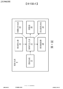
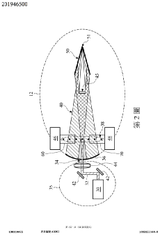
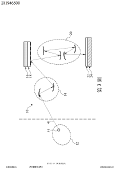
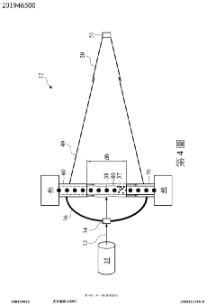
PatentActiveTW201946500A
Innovation
- Implementing a gas barrier around the droplet stream in the EUV light source device using a gas injection system and vacuum exhaust system to contain evaporated particles, combined with component biasing to repel or attract charged particles, thereby reducing contamination.
Environmental Regulations for Semiconductor Manufacturing
The semiconductor manufacturing industry operates under an increasingly stringent regulatory framework designed to minimize environmental impact and protect public health. These regulations encompass air quality standards, water discharge limits, chemical handling protocols, and waste management requirements that directly influence EUV lithography operations.
Air quality regulations impose strict limits on volatile organic compounds (VOCs), particulate matter, and hazardous air pollutants emitted from semiconductor facilities. EUV lithography systems must comply with National Emission Standards for Hazardous Air Pollutants (NESHAP) in the United States, similar standards under the European Union's Industrial Emissions Directive, and comparable regulations in Asia-Pacific regions. These standards require continuous monitoring of emissions and implementation of best available control technologies.
Water discharge regulations govern the treatment and disposal of process wastewater containing photoresist developers, cleaning solvents, and other chemicals used in EUV processes. The Clean Water Act in the US, Water Framework Directive in Europe, and national water protection laws in manufacturing regions establish maximum allowable concentrations for specific contaminants and mandate pretreatment before discharge to municipal systems.
Chemical management regulations, including REACH in Europe, TSCA in the United States, and similar frameworks globally, require comprehensive registration, evaluation, and authorization of chemical substances used in EUV lithography. These regulations mandate detailed safety data sheets, exposure assessments, and risk management measures for photoresists, cleaning agents, and process gases.
Waste management regulations classify and control the disposal of hazardous and non-hazardous waste streams from EUV operations. The Resource Conservation and Recovery Act (RCRA) in the US and the Waste Framework Directive in Europe establish cradle-to-grave tracking systems for hazardous waste, requiring proper characterization, storage, transportation, and disposal through licensed facilities.
Emerging regulations focus on greenhouse gas emissions, energy efficiency standards, and circular economy principles. Carbon pricing mechanisms and mandatory emissions reporting are becoming prevalent, while extended producer responsibility frameworks increasingly require manufacturers to consider product lifecycle environmental impacts.
Compliance with these evolving regulations necessitates proactive environmental management systems, regular auditing, and continuous improvement in process efficiency and waste reduction strategies within EUV lithography operations.
Carbon Footprint Reduction Strategies in EUV Fabs
EUV lithography facilities represent some of the most energy-intensive manufacturing environments in the semiconductor industry, with individual scanners consuming up to 1 MW of power during operation. The carbon footprint of these facilities extends beyond direct energy consumption to encompass complex supply chains, specialized infrastructure requirements, and sophisticated environmental control systems necessary for maintaining the ultra-clean conditions required for EUV processing.
The primary carbon emission sources in EUV fabs stem from the extreme power requirements of EUV light sources, which typically operate at only 2-5% efficiency, converting most input energy into waste heat. Additionally, the extensive cooling systems, cleanroom air filtration, and vacuum maintenance systems contribute significantly to overall energy consumption. Indirect emissions arise from the production and transportation of specialized consumables, including photoresists, masks, and ultra-pure chemicals.
Energy optimization strategies focus on implementing advanced power management systems that can dynamically adjust scanner power consumption during idle periods and optimize tool utilization schedules. Heat recovery systems capture waste heat from EUV sources and redirect it for facility heating or other thermal processes, potentially reducing overall energy demand by 15-20%. Smart grid integration allows fabs to shift energy-intensive operations to periods when renewable energy availability is highest.
Process efficiency improvements target reducing the number of exposure passes required through advanced computational lithography techniques and improved resist sensitivity. Multi-patterning optimization algorithms minimize the total number of lithographic steps while maintaining pattern fidelity, directly correlating to reduced energy consumption per wafer processed.
Facility-level carbon reduction initiatives include on-site renewable energy generation through solar installations and wind power integration where feasible. Energy storage systems enable load balancing and peak shaving, reducing reliance on carbon-intensive grid power during high-demand periods. Advanced building management systems optimize HVAC operations, lighting, and auxiliary equipment based on real-time occupancy and production schedules.
Supply chain decarbonization involves partnering with suppliers committed to renewable energy adoption and implementing circular economy principles for consumable materials. Local sourcing strategies reduce transportation-related emissions, while advanced recycling programs for silicon wafers and chemical recovery systems minimize waste generation and associated carbon impacts.
Unlock deeper insights with PatSnap Eureka Quick Research — get a full tech report to explore trends and direct your research. Try now!
Generate Your Research Report Instantly with AI Agent
Supercharge your innovation with PatSnap Eureka AI Agent Platform!